

“Digital Systems Testing and Design for Testability ”
Prof. Dr. V.N.Yarmolik
Lecture course: 32 hours lectures, 32 hours lab. works
3. Design for Testability
1

3.Design for Testability of Digital Circuits
3.1.Practical Rules
Ad Hoc Logic Techniques for testability enhancement
Feature |
Ad hoc technique |
Unknown initial state |
Initialization circuitry |
Internal clock |
Circuitry to disconnect internal clock and substitute |
|
tester clock |
Feedback loops |
Circuitry to permit tester to break feedback loop |
Deep sequential circuits |
Circuitry to segment circuits into more easily controlled |
(counter and divider chains) |
portions |
Wired logic |
Avoid |
Fan in and fan out points |
Add test access to these points |
2
3.Design for Testability of Digital Circuits
3.1.Practical Rules
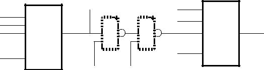
Rule #1. To maximize the controllability and observability of the digital circuit
A high controllability is achieved due to the fact that any circuit’s node can be easily set to any desired level (0 or 1). High observability is achieved when the state of any node in the circuit can be easily defined by its external nodes.
To improve the control and observation features of the circuit under test the following methods may be used:
1.Extra Gates Incorporation to improve Testability Measure
2.Extra Input\Output Pins Implementation for the Test Purpose Only
3.Logic and Mechanical adapter application to get the access to uncontrolled internal circuit’s feedback loops.
|
External output |
F2 |
|
F1 |
|
||
& |
& |
||
... |
|||
|
... |
External input
3
3.Design for Testability of Digital Circuits
3.1.Practical Rules
Rule #2. Delete or minimize logical redundancy
|
|
|
|
U 0 |
|
|
|
|
|
U 2 |
|
|
|
|
Inp ut0 |
|
|
|
|
|
|
|
|
|
|
|
|
|
O u tp ut0 |
|
|
|
|
|
|
|
|
|
|
|
|
|
||
|
|
IN1 |
Y |
|
|
|
|
IN1 |
Y |
|
||||
|
|
|
|
|
|
|
|
|
|
|||||
Inp ut1 |
|
|
|
IN2 |
|
|
|
|
|
IN2 |
|
|
|
|
|
|
|
|
|
|
|
|
|
|
|
|
|||
|
|
|
|
|
|
|
|
|
|
|
|
|
||
|
|
|
|
|
|
|
|
|
|
|
|
|
|
|
|
|
|
|
an d 2 |
|
|
|
|
|
or2 |
|
|
|
|
|
|
|
|
U 1 |
|
|
|
|
|
|
|
|
|
|
IN1 Y
\not\
U0 - AND gate; U1 – NOT gate; OR – gate.
The input node IN2 of the Gate 2AND (U0) is the redundant node. Due to this redundancy Stack-at 1 at this node is not detected by any input patterns.
4

3.Design for Testability of Digital Circuits
3.1.Practical Rules
The following example shows the redundant circuit. This circuit is described by the expression F(x1,x2,x3)= x1x2+ x1x3+x2x3= x1x2+x1x3 . In fact, the value of
F(x1,x2,x3) is determined by only the values of two first terms and is independent of
x2x3 |
|
|
|
|
|
|
|
|
|
|
U3 |
|
|
|
|
|
|
|
|
|
|
x 1 |
|
|
|
|
|
|
|
|
|
|
|
|
|
|
|
|
|
|
|
|
|
|
|
|
|
|
|
|
|
|
IN1 |
Y |
|
|
|
|
|
|
|
|
|
||
|
|
|
|
|
|
|
|
|
|
|
|
|
|
|
|
|
|
|
|||
|
|
|
|
|
|
|
|
|
|
|
|
|
|
|
|
|
|
|
|
||
|
x 2 |
|
|
|
|
|
|
|
|
|
IN2 |
|
|
|
|
|
|
|
|
|
|
|
|
|
|
|
|
|
|
|
|
|
|
|
|
|
|
|
|
|
|
||
|
|
|
|
|
|
|
|
|
|
|
|
|
|
|
|
|
|
|
|
|
|
|
|
|
|
|
|
|
|
|
|
|
|
|
|
|
|
|
U1 |
|
|
|
|
|
|
|
|
|
|
|
|
|
|
|
nand2 |
|
|
|
|
|
|||||
|
|
|
|
|
|
|
|
|
|
|
|
|
|
|
|
|
|
|
|
|
|
|
|
|
|
|
|
U0 |
|
|
|
|
U4 |
|
|
|
|
|
IN1 Y |
|
|
|
F |
|
|
|
|
|
|
|
|
|
|
|
|
|
|
|
|
|
|
|
|
||
|
|
|
|
|
|
IN1 |
Y |
|
|
IN1 |
Y |
|
|
|
|
IN2 |
|
|
|
|
|
|
|
|
|
|
|
|
|
|
|
|
|
||||||||||
|
|
|
|
|
|
|
|
|
|
|
IN2 |
|
|
|
|
|
IN3 |
|
|
|
|
|
x 3 |
|
|
|
|
\not\ |
|
|
|
|
|
|
|
|
|
|
|
|
|||
|
|
|
|
|
|
|
|
|
|
|
|
|
|
|
|
|
|
|
|
||
|
|
|
|
|
|
|
|
|
|
|
|
|
|
|
|
|
|
|
|
||
|
|
|
|
|
|
|
|
|
nand2 |
|
|
|
|
|
nand3 |
|
|
|
|
||
|
|
|
|
|
|
|
|
|
|
|
|
|
|
|
|
|
|
|
|
||
|
|
|
|
|
|
|
|
|
|
|
U5 |
|
|
|
|
|
|
|
|
|
|
|
|
|
|
|
|
|
|
|
|
|
|
|
|
|
|
|
|
|
|
|
|
|
|
|
|
|
|
|
|
|
|
|
IN1 |
Y |
|
|
|
|
|
|
|
|
|
|
|
|
|
|
|
|
|
|
|
|
|
|
|
|
|
|
|
|
|
||
|
|
|
|
|
|
|
|
|
|
|
IN2 |
|
|
|
|
|
|
|
|
|
|
|
|
|
|
|
|
|
|
|
|
|
|
|
|
|
|
|
|
|
|
|
|
|
|
|
|
|
|
|
|
|
|
|
|
|
|
|
|
|
|
|
|
|
|
|
|
|
|
|
|
|
|
|
|
|
nand2 |
|
|
|
|
|
|
|
|
|
|
|
The presence of logically redundant nodes may cause racing or masking on |
||||||||||||||||||||
non-redundant nodes in the circuit. Thus, with fault U5 stuck-at 1 and the change of variable x1 from 1 to 0, for the case when x2=x3=1 an intermittent negative pulse
may occur causing the racing. |
5 |

3.Design for Testability of Digital Circuits
3.1.Practical Rules
The fault at the redundant node may mask the fault at the another node. The following example shows that the fault stuck-at 1 at the third input (IN3) of the gate U4 is undetectable due to the redundancy, as well as the fault stuck-at 0 at the second input (IN2) of the gate U3 is detectable by the pattern x1x2x3=110. In a case when the faults for the gates U3 and U4 are present both the above mention test does not detect the fault for the gate U3.
|
|
|
|
|
|
|
|
|
|
|
U 4 |
|
|
|
|
|
|
|
|
|
|
X1 |
|
|
|
|
|
|
|
|
|
|
|
|
|
|
|
|
|
|
|
|
|
|
|
|
|
|
|
|
|
|
|
IN1 |
Y |
|
|
|
|
|
|
|
|
|
|
|
|
|
|
|
|
|
|
|
|
|
|
|
|
|
|
|
|
|
|||
X2 |
|
|
|
|
|
|
|
|
|
|
IN2 |
|
|
|
|
|
|
|
|
|
|
|
|
|
|
|
|
|
|
|
|
|
|
|
|
|
|
|
|
|
|
||
X3 |
|
|
|
|
|
|
|
|
|
|
IN3 |
|
|
|
|
|
|
|
|
|
|
|
|
|
|
|
|
|
|
|
|
|
|
|
|
|
|
|
|
|
|
||
|
|
|
|
|
|
|
|
|
|
|
|
|
|
|
|
|
|
|
|
|
|
|
|
|
|
|
|
|
|
|
|
|
na n d3 |
|
|
|
|
|
U 5 |
|
|
|
|
|
|
|
|
|
U 0 |
|
|
|
|
|
U 2 |
|
|
|
|
|
|
|
|
|
O u tp ut0 |
|
|
|
|
|
|
|
|
|
|
|
|
|
|
|
IN1 |
Y |
|
|
|||
|
|
|
|
|
|
|
|
|
|
|
|
|
|
|
|
|
|
|
|||
|
|
|
|
|
IN1 |
Y |
|
|
|
|
IN1 |
Y |
|
|
|
|
IN2 |
|
|
|
|
|
|
|
|
|
|
|
|
|
|
|
|
|
|||||||||
|
|
|
|
|
|
|
|
|
|
|
IN2 |
|
|
|
|
|
IN3 |
|
|
|
|
|
|
|
|
|
\no t\ |
|
|
|
|
|
|
|
|
|
|
|
|
|
|||
|
|
|
|
|
|
|
|
|
|
|
|
|
|
|
|
|
|
|
|
|
|
|
|
|
|
|
|
|
|
|
|
|
|
|
|
|
|
|
|
|
|
|
|
|
|
|
|
|
|
|
|
|
|
|
na n d2 |
|
|
|
|
|
a n d 3 |
|
|
|
|
|
|
|
|
|
U 1 |
|
|
|
|
|
U 3 |
|
|
|
|
|
|
|
|
|
|
|
|
|
|
|
|
|
|
|
|
|
|
|
|
|
|
|
|
|
|
|
|
|
|
|
|
|
IN1 |
Y |
|
|
|
|
IN1 |
Y |
|
|
|
|
|
|
|
|
|
|
|
|
|
|
|
|
|
|
|
|
|
|
|
|
|
||||||
|
|
|
|
|
|
|
|
|
|
|
IN2 |
|
|
|
|
|
|
|
|
|
|
|
|
|
|
|
\no t\ |
|
|
|
|
|
|
|
|
|
|
|
|
|
|
|
|
|
|
|
|
|
|
|
|
|
|
|
|
|
|
|
|
|
|
|
|
|
|
|
|
|
|
|
|
|
|
|
|
|
|
|
|
|
|
|
|
|
|
|
|
|
|
|
|
|
|
|
|
|
|
|
na n d2 |
|
|
|
|
|
|
|
|
|
|
6

3.Design for Testability of Digital Circuits
3.1.Practical Rules
Rule #3. To provide breaking feedback loops.
Uncontrollable feedback loops are the source of some problems at test generation and fault simulation.

 &
& 
 &
& 
 &
&
Combinational logic may not have a feedback loop unless the feedback loop goes via a flip-flop.
Rule #4. Non-three-state driver.
If a signal is driven by more than one driver, the drivers must be of the three- state-type.
7
3.Design for Testability of Digital Circuits
3.1Practical Rules
Rule #5. All unused inputs of the gates must be connected to the appropriate points (Power supply or ground)
Rule #6. Complex digital circuits should be partitioning into smaller subcircuits to reduce the test generation complexity.
The test generation complexity for deterministic methods can be approximate by the equation:
Cdeterm. Alg. = k2L3
And for the random search approach:
CRandom Search = k1L2;
Rule #7. The digital and analogue modules in the system must be kept physically apart. This rule may be explained by the fact that the strategy of analogue circuit testing is substantially different from that for testing and diagnosing digital circuits.
8

3.Design for Testability of Digital Circuits
3.1.Practical Rules
Rule #8. All clocks used in a circuit design must be controllable and testable by external inputs and outputs of the circuit.
Clk |
|
|
|
|
|
|
Clk_i |
Clk |
|
|
|
|
|
|
|
Clk |
|
||||
|
|
|
|
|
|
|
|
|||
|
|
|
|
|
|
d |
|
|
d |
|
|
|
|
|
|
|
|
|
|
||
|
|
|
|
|
|
|
|
|
|
|
|
|
|
|
|
|
|
|
|
|
|
Rule #9. The clock may not be connected, either directly or via combinational logic, to the d-input of the internal flip-flops.
Clk |
|
|
|
|
|
|
|
|
|
|
|
en |
|
|
|
& |
|
|
Clk |
|
|
|
|
|
|
|
|
|
||||
|
|
|
|
|
|
|
||||
|
|
|
|
|
|
|
||||
|
|
|
|
|
|
|
|
d |
|
|
|
|
|
|
|||||||
|
|
|
|
|
a |
|
||||
|
|
|
|
|
|
|
|
|
||
|
|
|
|
|
|
|
|
|
||
Rule #10. It must be possible to control the asynchronous reset for all the internal flip-flops from an input on the circuit.
Rule # … .
9

3.Design for Testability of Digital Circuits
3.1.Testable VHDL code
Combinational feedback loops.
ATPG does not normally support asynchronous design. This means that combinational feedback loops are not permissible.
Example: Suppose that we synthesize the following VHDL code d<=d+a; A signal d is on both sides of the assignment symbol (<=), a combinational feedback loop is obtained. The solution is to break the combinational feedback loop with a flip-flop. The VHDL code can then be written as follows:
Process(clk,resetn) begin
if resetn=‘0’ then q_loop<=(other=>’0’);
elsif clk’event and clk=‘1’ then q_loop<=q;
end if; End process;
|
|
|
|
|
q_loop |
|
|
|
||
clk |
|
|
|
|
|
|
|
|
|
|
clk |
|
|
|
|
|
|
||||
|
|
|
|
|
|
|
|
|
||
|
|
|
d |
|
+ |
|
q |
|
||
a |
|
|
|
|||||||
|
|
|
|
|
||||||
|
|
|
||||||||
|
|
|
|
|||||||
resetn |
|
|
|
|
|
10 |
|
|
||
|
|
|
|
|
|
|
||||
|
|
|
|
|
|
|
|
|
|
|
|
|
|
|
|
|
|
|
|
|
|
|
|
|
|
|
|
|
|
|
|
|
q<=q_loop + a;