

ЦОС_Заочники2013 / Курсовая МПиЦОС 2011 / Справочная информация / TI / TMS 320 / Толковый обзор всего семейства
.pdfTMS320C20x ESSP Block Diagram
|
|
Data bus |
|
||
Control |
Receive (±3) |
Transmit (±3) |
|
||
Receive (±2) |
Transmit (±2) |
Control |
|||
logic |
logic |
||||
|
|
|
|||
(receive) |
Receive (±1) |
Transmit (±1) |
(transmit) |
||
|
|
|
|||
|
Receive |
(0) |
Transmit (0) |
|
|
RINT |
|
|
|
XINT |
|
|
RSR |
|
XSR |
|
|
CLKR |
|
|
CLKX |
DR |
FSR |
FSX |
DX |
The Leader in DSP Solutions - 21

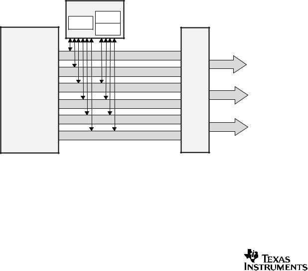
TMS320C20x Asynchronous Serial Port
The TMS320C20x offers an asynchronous serial port that is full-duplex and double-buffered. It accepts 8-bit data and can be programmed via a register to accept baud rates of up to 2.5 Mbps. The asynchronous serial port can be used to communicate with other devices such as microcontrollers or for RS-232 connections supporting data transfers of up to 250.0 bps.
Features included with the 'C20x asynchronous serial port are:
SFull duplex
SDouble buffered
S8-bit data transfers
S16-bit register for baud-rate generation
SBaud rates up to 2.5 Mbps (@ 25-ns instruction cycle time)
SSerial-peripheral interface (SPI) module, multi-channel
All 'C2xx devices, except the 'C209, feature this asynchronous serial port.
The Leader in DSP Solutions - 22

TMS320C20x Asynchronous Serial Port Block Diagram
Data bus
Control
logic
(receive)
TXRXINT
Sequence |
control |
ADTR (8) |
ARSR (8) |
ADTR (8) |
Control |
|
logic |
||
|
||
|
(transmit) |
|
|
TXRXINT |
AXSR (8) |
Sequence |
control |
Baud rate generator
RX |
CLKOUT1 |
TX |
The Leader in DSP Solutions - 23

TMS320C2xx Memory Bus
The 'C2xx advanced Harvard-type architecture maximizes processing power by maintaining two separate memory bus structures, program and data, for full-speed execution. This multiple bus structure allows reading both data and instructions simultaneously. Instructions support data transfers between the two spaces. This architecture lets you store coefficients in program memory to be read in RAM, eliminating the need for a separate coefficient ROM. This, coupled with a 4-level-deep pipeline, allows the TMS320C2xx to execute most instructions in a single cycle.
The 'C2xx dual-access RAM (DARAM) allows writes-to and reads-from the RAM in the same cycle without the address restrictions of SARAM. The dual-access RAM is configured in three blocks: block B0, block B1, and block B2. Block B0 is a 256-word block that can be configured as data or program memory. Block B1 is 256 words in data memory and block B2 is 32 words in data memory.
Some 'C2xx devices also have single-access RAM (SARAM) and/or ROM. Additionally, the 'F206 has flash memory.
The ability of the DARAM to perform two accesses in one cycle, coupled with the parallel nature of the 'C2xx architecture, enables the 'C2xx devices to perform three concurrent memory accesses in any given machine cycle.
The Leader in DSP Solutions - 24
TMS320C2xx Memory Bus Block Diagram
Dual-access RAM |
|
||
|
B1 |
|
|
B0 |
256x 16 |
|
|
256x 16 |
B2 |
|
|
|
32x 16 |
|
|
|
Program address |
|
|
|
|
Address |
|
|
Program data |
External |
|
TMS320C2xx |
Data read address |
logic |
|
CPU |
|||
|
Data |
||
|
Data read data |
interface |
|
|
|
||
|
Data write address |
|
|
|
|
Control |
|
|
Data write data |
|
|
The Leader in DSP Solutions - 25

TMS320C20x Generation Summary
All TMS320C20x devices share the same CPU architecture and accept source code from all 'C1x, 'C2x, and 'C2xx devices. This table gives a 'C20x generation product summary so that you can choose the best combination of performance, memory, power, package, and peripherals for your system.
The Leader in DSP Solutions - 26

TMS320C20x Generation Summary Table
|
|
On-Chip Memory |
Memory |
Serial Ports |
I/O |
|
|
|
||||||
|
|
|
(Words) |
|
|
|
|
|
||||||
|
|
|
|
|
|
|
|
|
|
|
|
|
|
Package |
Product |
MIPS |
RAM |
ROM |
|
Flash |
Off-Chip |
Sync |
Async |
Parallel |
DMA |
||||
|
(TQFP) |
|||||||||||||
|
|
|
|
|
|
|
|
|
|
|
|
|
|
|
TMS320C203 |
20/28.5/40 |
544 |
± |
|
± |
|
64K/64K |
1 |
1 |
64K x 16 |
Ext. |
100 |
||
TMS320LC203 |
20 |
|
|
|
± |
|
64K/64K |
|
|
64K x 16 |
|
Ext. |
|
|
544 |
± |
|
|
1 |
1 |
|
|
100 |
||||||
|
|
|
|
|
|
|
|
|
|
|
|
|
|
|
TMS320F206 |
20 |
4.5K |
± |
|
32K |
|
64K/64K |
1 |
1 |
64K x 16 |
|
Ext. |
|
100 |
TMS320C206 |
40 |
4.5K |
32K |
|
± |
|
64K/64K |
1 |
1 |
64K x 16 |
Ext. |
100 |
||
TMS320LC206 |
40 |
4.5K |
32K |
|
|
|
64K/64K |
1 |
1 |
64K x 16 |
Ext. |
100 |
||
|
|
|
|
|
|
|
|
|
|
|
|
|
|
|
TMS320C209 |
20/28.5 |
4.5K |
4K |
|
± |
|
64K/64K |
± |
± |
64K x 16 |
± |
|
80 |
|
The Leader in DSP Solutions - 27

TMS320C24x Features
The features for 'C24x are:
SProcessing hardware
±32-bit arithmetic logic unit (CALU)
±32-bit accumulator
±16-bit 16-bit parallel multiplier with a 32-bit product capability
±Three scaling shifters
±Eight 16-bit auxiliary registers with a dedicated arithmetic unit for indirect addressing of data memory
SMemory
±192K words 16-bit maximum addressable memory space
±On-chip dual-access RAM (DARAM)
±On-chip ROM or flash memory
±External memory interface module with software wait state, 16-bit address lines, and 16-bit data lines
±Support of hardware wait states
SProgram control
±Four-level pipeline operation
±Eight-level hardware stack
±User-maskable interrupts
The Leader in DSP Solutions - 28

TMS320C24x Features (continued)
SInstruction set
±Single-instruction repeat operation
±Single-cycle multiply/accumulate instructions
±Memory block move instructions for program/data management
±Indexed-addressing capability
±Bit-reversed indexed-addressing capability for radix-2 FFTs
SPower
±Static CMOS technology
±Four power-down modes to reduce power consumption
SEmulation: IEEE Standard 1149.1 boundary-scan logic interfaced to on-chip scan-based emulation logic
SSpeed: 50-ns instruction cycle time, with most instructions single cycle
SCode compatibility with TMS 320 fixed-point devices
±Source code compatible with the 'C25 and 'C2xx devices, and upwardly compatible with the 'C5x generation of DSPs
SOn-chip peripherals
The Leader in DSP Solutions - 29

TMS320C240/F240
These are key features of the 'C240x and 'F240x:
SHigh-performance static CMOS technology
SIncludes the T320C2xLP core CPU
±Source code compatible with TMS320C25;
±Upwardly compatible with TMS320C5x
±50-ns instruction cycle time
SMemory
±544K words 16-bits of on-chip data/program dual-access RAM
±16K words 16 bits of on-chip program ROM ('C240) / flash memory ('F240)
±192K words 16 bits of total memory address reach
SEvent-manager module (12 PWM outputs)
SDual 10-bit analog-to-digital conversion module
S28 individually programmable, multiplexed I/O pins
SPhase-locked loop (PLL)-based clock module
SWatchdog timer module (with real-time interrupt)
SSerial communication interface (SCI) module
SSerial peripheral interface (SPI) module
SSix external interrupts
SFour power-down modes for low-power operation
SScan-based emulation
SExtended temperature range options available
The Leader in DSP Solutions - 30