

- •Preface
- •About This Manual
- •Audience
- •Manual Organization
- •Suggested Reading
- •Manual Conventions
- •1.1 Introduction
- •1.2 56800E Core Description
- •1.3 56852 Architectural Overview
- •1.4 System Bus Controller
- •1.5 56852 Memory
- •1.6 56852 Peripheral Blocks
- •2.1 Introduction
- •2.2 Features
- •2.3 Signal and Package Information
- •3.1 Introduction
- •3.2 Program Boot ROM
- •3.3 Memory Map
- •4.1 Introduction
- •4.2 Features
- •4.3 SIM Block Diagram
- •4.4 Signal Description
- •4.5 Module Memory Map
- •4.6 Register Descriptions (SYS_BASE = $1FFF08)
- •4.7 Implementation
- •4.8 Generated Clocks
- •4.9 Generated Resets
- •4.10 Power Mode Controls
- •5.1 Introduction
- •5.2 Features
- •5.3 Functional Description
- •5.4 Block Diagram
- •5.5 Module Memory Map
- •5.6 Register Descriptions (EMI_BASE = $1FFE40)
- •5.7 Timing Specifications
- •5.8 Clocks
- •5.9 Interrupts
- •5.10 Resets
- •6.1 Introduction
- •6.2 OSC (Oscillator) Circuit Detail
- •6.3 Phase Locked Loop (PLL) Circuit Detail
- •6.4 CGM Functional Detail
- •6.5 Module Memory Map
- •6.6 Register Descriptions (CGM_BASE = $1FFF10)
- •6.7 OCCS Resets
- •6.8 OCCS Interrupts
- •7.1 Introduction
- •7.2 Features
- •7.3 Block Diagram
- •7.4 Method of Operation
- •7.5 Computer Operating Properly (COP) Module
- •7.6 Operating Modes
- •7.7 Block Diagram
- •7.8 Module Memory Map
- •7.9 Register Descriptions (COP_BASE = $1FFFD0)
- •7.10 Clocks
- •7.11 Resets
- •7.12 Interrupts
- •8.1 Introduction
- •8.2 Features
- •8.3 ITCN Module Signal Description
- •8.4 Block Diagram
- •8.5 Functional Description
- •8.6 Operating Modes
- •8.7 Wait and Stop Modes Operations
- •8.8 Module Memory Map
- •8.9 Register Descriptions (ITCN_BASE = $1FFF20)
- •8.10 Resets
- •8.11 Interrupts
- •9.1 Introduction
- •9.2 Features
- •9.3 Block Diagram
- •9.4 Signal Descriptions
- •9.5 Functional Description
- •9.6 Low Power Modes
- •9.7 Module Memory Map
- •9.8 Register Descriptions (SCI_BASE = $1FFFE0)
- •9.9 Clocks
- •9.10 Resets
- •9.11 Interrupts
- •10.1 Introduction
- •10.2 Features
- •10.3 SPI Block Diagram
- •10.4 Signal Descriptions
- •10.5 External I/O Signals
- •10.6 Operating Modes
- •10.7 Transmission Formats
- •10.8 Transmission Data
- •10.9 Error Conditions
- •10.10 Module Memory Map
- •10.11 Registers Descriptions (SPI_BASE = $1FFFE8)
- •10.12 Resets
- •10.13 Interrupts
- •11.1 Introduction
- •11.2 Features
- •11.3 Signal Descriptions
- •11.4 Block Diagram
- •11.5 ISSI Configurations
- •11.6 Module Memory Map
- •11.7 Register Descriptions (ISSI_BASE = $1FFE20)
- •11.8 ISSI Operating Modes
- •11.9 Clocks
- •11.10 Clock Operation Description
- •11.11 Resets
- •11.12 Interrupts
- •11.13 User Notes
- •12.1 Introduction
- •12.2 Features
- •12.3 Operating Modes
- •12.4 Block Diagram
- •12.5 Signal Description
- •12.6 Functional Description
- •12.7 Counting Modes Definitions
- •12.8 Module Memory Map
- •12.9 Register Descriptions (TMR_BASE = $1FFE80)
- •12.10 Resets
- •12.11 Interrupts
- •13.1 Introduction
- •13.2 Features
- •13.3 GPIO Block Diagram
- •13.4 Functional Description
- •13.5 Modes of Operation
- •13.6 GPIO Configurations
- •13.7 Module Memory Maps
- •13.8 Register Descriptions
- •13.9 Data Register Access
- •13.10 Resets
- •13.11 Interrupts
- •14.1 Introduction
- •14.2 Features
- •14.3 Master Test Access Port (TAP)
- •14.4 TAP Block Diagram
- •14.5 JTAG Port Architecture
- •14.6 JTAG Bypass Register (JTAGBR)
- •14.7 JTAG Boundary Scan Register (BSR)
- •14.8 TAP Controller
- •14.9 56852 Restrictions
- •B.1 Introduction
- •B.2 Programmer’s Sheets

Features
10.1 Introduction
This chapter describes the Serial Peripheral Interface (SPI) module. The module allows full-duplex, synchronous, serial communication between the controller and peripheral devices, including other controllers. Software can poll SPI status flags or SPI operation can be interrupt driven. This block contains four 16-bit memory mapped registers for control parameters, status, and data transfer.
10.2 Features
Features of the SPI module include:
•Full-duplex operation
•Master and slave modes
•Double-buffered operation with separate transmit and receive registers
•Programmable length transmissions (2 to 16 bits)
•Programmable transmit and receive shift order (MSB first or last bit transmitted)
•Eight master mode frequencies (maximum = bus frequency 2)
•Maximum slave mode frequency = bus frequency
•Clock ground for reduced radio frequency (RF) interference
•Serial clock with programmable polarity and phase
•Two separately enabled interrupts
—SPRF (SPI Receiver Full)
—SPTE (SPI Transmitter Empty)
•Mode fault error flag interrupt capability
•Wired OR mode functionality to enabling connection to multiple SPIs
|
Serial Peripheral Interface (SPI), Rev. 4 |
Freescale Semiconductor |
10-3 |
-packaged product lines and part numbers indicated here currently are not |
2010: MC13892 |
Commission, BGA |
prior to September |
order from the United States International Trade Freescale for import or sale in the United States |
|
of an from |
|
Because |
available |

SPI Block Diagram
10.3 SPI Block Diagram
IPBus PERIPHERAL BUS
CLK
(From IPBus)
|
|
|
2 |
|
|
|
Clock |
8 |
|
||
|
Divider |
16 |
|
||
|
|
|
32 |
|
|
|
|
|
|
|
|
|
|
|
|
|
|
SPMSTR |
SPE |
|
|||
|
|
|
|
|
|
|
Transmit Data Register |
|
|
Shift Register |
|
|
2–16 Bits |
MISO |
|
|
MOSI |
|
Receive Data Register |
|
|
|
Pin |
|
|
Control |
|
|
Logic |
Clock |
SCLK |
|
Select |
M |
|
|
Clock |
|
|
Logic |
S |
SPR1 |
SPR0 |
SS |
|
||
|
|
|
|
|
|
|
|
|
|
|
|
|
|
|
|
|
|
|
|
|
|
|
|
|
|
|
|
|
|
|
|
|
|
|
|
|
|
|
|
|
|
|
|
|
|
|
|
SPMSTR |
|
CPHA |
CPOL |
|
|
||||||
|
|
|
|
|
|
|
|
|
|
|
||||
|
|
|
|
|
|
|
|
|
|
|
|
|
|
|
|
|
|
|
|
|
|
|
|
|
|
|
|
|
|
|
|
|
|
|
|
|
|
|
|
|||||
Transmitter |
|
|
|
|
MODFEN |
|
|
|
|
|
|
|||
|
|
|
|
|
|
|
|
|
|
|||||
|
|
|
|
|
|
|
|
|
|
|
|
|
|
|
Interrupt Request |
SPI |
|
|
|
|
ERRIE |
|
|
|
|
||||
|
|
|
|
|
|
|
|
|
|
|||||
|
|
|
|
|
|
|
|
|
|
|
|
|
|
|
|
|
|
|
|
SPTIE |
|
|
|
|
|
|
|||
|
Control |
|
|
|
|
|
|
|
|
|||||
|
|
|
|
|
|
|
||||||||
Receiver / Error |
|
|
|
|
|
SPRIE |
|
|
|
|
||||
|
|
|
|
|
|
|
||||||||
Interrupt Request |
|
|
|
|
|
|
|
|
|
|
|
|
|
|
|
|
|
|
|
DSO |
|
|
|
|
|
|
|||
|
|
|
|
|
|
|
|
|
|
|
|
|||
|
|
|
|
|
|
SPE |
|
|
|
|
|
|
||
|
|
|
|
|
|
|
|
|
|
|
|
|||
|
|
|
|
|
|
|
|
|
|
|
|
|
|
|
SPRF
SPTE
OVRF
MODF
Figure 10-1. SPI Block Diagram
10.4 Signal Descriptions
10.4.1 Master In/Slave Out (MISO)
MISO is one of the two SPI module pins dedicated to transmit serial data. In full duplex operation, the MISO pin of the master SPI module is connected to the MISO pin of the slave SPI module. The master SPI simultaneously receives data on its MISO pin and transmits data from its MOSI pin.
|
56852 Digital Signal Controller User Manual, Rev. 4 |
10-4 |
Freescale Semiconductor |
-packaged product lines and part numbers indicated here currently are not |
2010: MC13892 |
Commission, BGA |
prior to September |
order from the United States International Trade Freescale for import or sale in the United States |
|
of an from |
|
Because |
available |
Signal Descriptions
Slave output data on the MISO pin is enabled only when the SPI is configured as a slave. The SPI is configured as a slave when the SPMSTR bit, illustrated in Figure 10-13, is Logic 0 and its SS pin is at Logic 0. To support a multiple slave system, a Logic 0 on the SS pin puts the MISO pin in a High-Z state.
10.4.2 Master Out/Slave In (MOSI)
MOSI is the other SPI module pin dedicated to transmit serial data. In full duplex operation, the MOSI pin of the master SPI module is connected to the MOSI pin of the slave SPI module. The master SPI simultaneously transmits data from its MOSI pin and receives data on its MISO pin.
10.4.3 Serial Clock (SCLK)
The serial clock synchronizes data transmission between master and slave devices. In a master controller, the SCLK pin is the clock output. In a slave controller, the SCLK pin is the clock input. In full duplex operation, the master and slave controller exchange data in the same number of clock cycles as the number of bits of transmitted data.
10.4.4 Slave Select (SS)
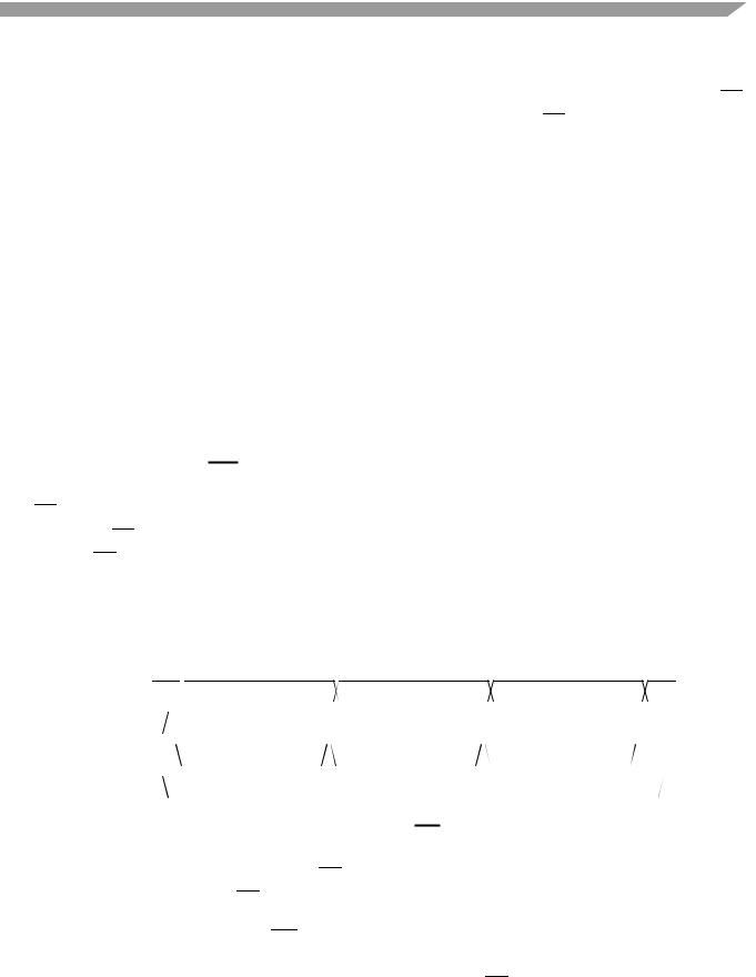
The SS pin has various functions depending on the current state of the SPI. For an SPI configured as a slave, the SS is used to select a slave. When the Clock Phase (CPHA) bit in the SPSCR is cleared, the SS is used to define the start of a transmission, so it must be toggled high and low between each full length data transmitted for the CPHA = 0 format. However, it can remain low between transmissions for the CPHA = 1 format as illustrated in Figure 10-2.
MISO/MOSI |
|
|
|
|
|
|
Data 1 |
|
|
Data 2 |
Data 3 |
|
|
|||||||||||||||
Master |
|
|
|
|
|
|
|
|
|
|
|
|
|
|
|
|
|
|
|
|
|
|
|
|
|
|
|
|
|
|
|
|
|
|
|
|
|
|
|
|
|
|
|
|
|
|
|
|
|
|
|
|
|
|
|
|
|
SS |
|
|
|
|
|
|
|
|
|
|
|
|
|
|
|
|
|
|
|
|
|
|
|
|
||||
Slave |
|
|
|
|
|
|
|
|
|
|
|
|
|
|
|
|
|
|
|
|
|
|
|
|
|
|
||
SS |
|
|
|
|
|
|
|
|
|
|
|
|
|
|
|
|
|
|
|
|
|
|
|
|
||||
|
|
|
|
|
|
|
|
|
|
|
|
|
|
|
|
|
|
|
|
|
|
|
|
|||||
(CPHA = 0) |
|
|
|
|
|
|
|
|
|
|
|
|
|
|
|
|
|
|
|
|
|
|
|
|
||||
Slave |
|
|
|
|
|
|
|
|
|
|
|
|
|
|
|
|
|
|
|
|
|
|
|
|
|
|
||
SS |
|
|
|
|
|
|
|
|
|
|
|
|
|
|
|
|
|
|
|
|
|
|
|
|
||||
|
|
|
|
|
|
|
|
|
|
|
|
|
|
|
|
|
|
|
|
|
|
|
|
|||||
(CPHA = 1) |
|
|
|
|
|
|
|
|
|
|
|
|
|
|
|
|
|
|
|
|
|
|
|
|
||||
Figure 10-2. CPHA/SS Timing
When an SPI is configured as a slave, the SS pin is always configured as an input. The MODFEN bit can prevent the state of the SS from creating a MODF error.
Note: A Logic 1 voltage on the SS pin of a slave SPI puts the MISO pin in a high impedance state. The slave SPI ignores all incoming SCLK clocks, even if it was already in the middle of a transmission. A mode fault occurs if the SS pin changes state during a transmission.
|
Serial Peripheral Interface (SPI), Rev. 4 |
Freescale Semiconductor |
10-5 |
-packaged product lines and part numbers indicated here currently are not |
2010: MC13892 |
Commission, BGA |
prior to September |
order from the United States International Trade Freescale for import or sale in the United States |
|
of an from |
|
Because |
available |

External I/O Signals
When an SPI is configured as a master, the SS input can be used in conjunction with the MODF flag to prevent multiple masters from driving MOSI and SCLK. For the state of the SS pin to set the MODF flag, the MODFEN bit in the SCLK register must be set.
Table 10-1. SPI I/O Configuration
SPE |
SPMSTR |
MODFEN |
SPI Configuration |
|
|
|
State of SS Logic |
|
|
|
|
|
|
|
|
|
|
|
|
|
|
|
|
0 |
X |
X |
Not Enabled |
|
|
|
ignored by SPI |
SS |
|||||||
1 |
0 |
X |
Slave |
Input-only to SPI |
|||
|
|
|
|
|
|
||
1 |
1 |
0 |
Master without MODF |
|
|
|
ignored by SPI |
SS |
|||||||
1 |
1 |
1 |
Master with MODF |
Input-only to SPI |
|||
|
|
|
|
|
|
|
|
X = Don’t care
10.5 External I/O Signals
There are four external SPI pins. Each is summarized in Table 10-2.
Table 10-2. External I/O Signals
Signal Name |
Description |
Direction |
||
|
|
|
||
|
|
|
||
MOSI |
Master-Out Slave-In Pad Pin |
Bi-Directional |
||
|
|
|
||
MISO |
Master-In Slave-Out Pad Pin |
Bi-Directional |
||
|
|
|
||
SCLK |
Slack Clock Pad Pin |
Bi-Directional |
||
|
|
|
|
|
|
|
|
Slave Select Pad Pin (Active Low) |
Input |
|
SS |
|||
|
|
|
|
|
10.6 Operating Modes
The SPI has two operating modes:
1.Master
2.Slave
An operating mode is selected by the SPMSTR bit in the SPSCR as follows:
•SPMSTR = 0 Slave mode
•SPMSTR = 1 Master mode
Note: The SPMSTR bit should be configured before enabling the SPI, setting the SPE bit in the SPSCR. The master SPI should be enabled before enabling any slave SPI. All slave SPIs should be disabled before disabling the master SPI.
|
56852 Digital Signal Controller User Manual, Rev. 4 |
10-6 |
Freescale Semiconductor |
-packaged product lines and part numbers indicated here currently are not |
2010: MC13892 |
Commission, BGA |
prior to September |
order from the United States International Trade Freescale for import or sale in the United States |
|
of an from |
|
Because |
available |

Operating Modes
10.6.1 Master Mode
The SPI operates in Master mode when the SPI master bit, SPMSTR, is set.
Note: Configure the SPI module as master or slave before enabling the SPI. Enable the master SPI before enabling the slave SPI. Disable the slave SPI before disabling the master SPI.
Only a Master SPI module can initiate transmissions. With the SPI enabled, software begins the transmission from the master SPI module by writing to the SPI Data Transmit Register (SPDTR). If the Shift Register is empty, the data immediately transfers to the Shift Register, setting the SPI Transmitter Empty (SPTE) bit. The data begins shifting out on the MOSI pin under the control of the SPI Serial Clock (SCLK).
The SPR1 and SPR0 bits in the SPSCR control the baud rate generator and determine the speed of the Shift Register. The baud rate generator of the master also controls the Shift Register of the slave peripheral via the SCLK pin.
As the data shifts out on the MOSI pin of the master, external data shifts in from the slave on the master’s MISO pin. The transmission ends when the SPI Receiver Full (SPRF) bit in the SPSCR becomes set. At the same time the SPRF becomes set, the data from the slave transfers to the SPI Data Receive Register (SPDRR). In a normal operation, SPRF signals the end of a transmission. Software clears the SPRF by reading the SPSCR register with SPRF set and then reading the SPI Data Receive register, SPDRR. Writing to the SPI Data Transmit register, SPDTR, clears the SPTE bit.
Figure 10-3 is an example configuration for a Full-Duplex Master-Slave Configuration. Having the SS bit of the Master controller held high is only necessary if MODFEN = 1. Tying the Slave controller SS bit to ground should only be executed if CPHA = 1.
|
|
Master Controller |
|
|
|
|
|
|
|
|
|
|
|
|
|
|
|
|
|
|
|
|
Slave Controller |
|
|||||
|
|
|
|
|
|
|
|
MISO |
|
|
|
|
|
|
|
|
|
MISO |
|
|
|
||||||||
|
|
|
|
|
|
|
|
|
|
|
|
|
|
|
|
|
|
|
|
||||||||||
|
|
Shift Register |
|
||||||||||||||||||||||||||
|
|
|
|
|
|
|
|
|
|
|
|
|
|
|
|
|
|
|
|
|
|
|
|
|
|
||||
|
|
|
MOSI |
|
|
|
|
|
|
|
|
|
MOSI |
|
|
|
|
|
|
|
|||||||||
|
|
|
|
|
|
|
|
|
|
|
|
|
|
|
|
|
|
|
|
|
|
|
|
||||||
|
|
|
|
|
|
|
|
|
|
|
|
|
|
|
|
|
|
|
|
|
|
|
|||||||
|
|
|
|
|
|
|
|
Shift Register |
|
||||||||||||||||||||
|
|
|
|
|
|
|
|
|
|
|
|
|
|
|
|
|
|
|
|
|
|
|
|
|
|
|
|||
|
|
|
|
|
|
|
|
SCLK |
|
|
|
|
|
|
|
|
|
SCLK |
|
|
|
||||||||
|
|
|
|
|
|
|
|
|
|
|
|
|
|
|
|
|
|
|
|
|
|
|
|
||||||
|
|
|
|
|
|
|
|
|
|
|
|
|
|
|
|
|
|
|
|
|
|
||||||||
|
|
|
|
|
|
|
|
|
|||||||||||||||||||||
|
|
|
|
|
|
|
|
|
|
|
|
|
|
|
|
|
|
|
|
|
|
|
|
|
|
|
|
|
|
|
|
Baud Rate |
|
|
|
|
|
|
|
|
|
|
|
|
|
|
|
|
|
|
|
|
|
|
|
|
|
|
|
|
|
|
|
|
|
SS |
|
|
|
|
|
|
|
|
|
SS |
|
|
|
|
|
|
|
||||||
|
|
Generator |
|
|
|
|
|
|
VDD |
|
|
|
|
|
|
||||||||||||||
|
|
|
|
|
|
|
|
|
|
|
|
|
|
|
|
|
|
|
|
|
|
|
|
||||||
|
|
|
|
|
|
|
|
|
|
|
|
|
|
|
|
|
|
|
|
|
|
||||||||
|
|
|
|
|
|
|
|
|
|
|
|
|
|
|
|
|
|
|
|
|
|
|
|
|
|
|
|
|
|
|
|
|
|
|
|
|
|
|
|
|
|
|
|
|
|
|
|
|
|
|
|
|
|
|
|
|
|
|
|
|
|
|
|
|
|
|
|
|
|
|
|
|
|
|
|
|
|
|
|
|
|
|
|
|
|
|
|
|
|
Figure 10-3. Full-Duplex Master/Slave Connections
|
Serial Peripheral Interface (SPI), Rev. 4 |
Freescale Semiconductor |
10-7 |
-packaged product lines and part numbers indicated here currently are not |
2010: MC13892 |
Commission, BGA |
prior to September |
order from the United States International Trade Freescale for import or sale in the United States |
|
of an from |
|
Because |
available |

Operating Modes
10.6.2 Slave Mode
The SPI operates in the Slave mode when the SPMSTR bit is cleared. While in the Slave mode, the SCLK pin acts as the input for the serial clock from the master controller. Before a data transmission occurs, the SS pin of the slave SPI must be at Logic 0. SS must remain low until the transmission is complete or a Mode Fault error occurs.
Note: The SPI must be enabled (SPE = 1) for slave transmissions to be received.
Note: Data in the transmitter Shift Register will be unaffected by SCLK transitions in the event the SPI is operating as a slave but is deselected.
In a slave SPI module, data enters the Shift Register under the control of the serial clock, SCLK, from the master SPI module. After a full length data transmission enters the Shift Register of a slave SPI, it transfers to the SPDRR and the SPRF bit in the SPSCR is set. If the Receive Interrupt Enable (SPRIE) bit in the SPSCR has been set, a receive interrupt is also generated. To prevent an overflow condition, slave software must read the SPDRR before another full length data transmission enters the Shift Register.
The maximum frequency of the SCLK for an SPI configured as a slave is the bus clock speed. The bus clock speed is twice as fast as the fastest master SCLK potential generation. Frequency of the SCLK for an SPI configured as a slave does not have to correspond to any particular SPI baud rate. The baud rate only controls the speed of the SCLK generated by an SPI configured as a master. Therefore, the frequency of the SCLK for an SPI configured as a slave can be any frequency less than or equal to the bus speed.
When the master SPI starts a transmission, the data in the slave Shift Register begins shifting out on the MISO pin. The slave can load its Shift Register with new data for the next transmission by writing to its Transmit Data Register. The slave must write to its Transmit Data Register at least one bus cycle before the master starts the next transmission. Otherwise, the data already in the slave Shift Register shifts out on the MISO pin. Data written to the slave Shift Register during a transmission remains in a buffer until the end of the transmission.
When the CPHA bit is set, the first edge of SCLK starts a transmission. When CPHA is cleared, the falling edge of SS starts a transmission.
Note: SCLK must be in the proper idle state before the slave is enabled to prevent SCLK from appearing as a clock edge.
|
56852 Digital Signal Controller User Manual, Rev. 4 |
10-8 |
Freescale Semiconductor |
-packaged product lines and part numbers indicated here currently are not |
2010: MC13892 |
Commission, BGA |
prior to September |
order from the United States International Trade Freescale for import or sale in the United States |
|
of an from |
|
Because |
available |