

- •List of Figures
- •List of Tables
- •List of Examples
- •About This Book
- •1.1 DSP56824 Architecture Overview
- •1.1.1 DSP56824 Peripheral Blocks
- •1.1.1.1 On-Chip Memory
- •1.1.1.2 External Memory Interface (Port A)
- •1.1.1.3 General-Purpose Input/Output Port (Port B)
- •1.1.1.4 Programmable I/O Port (Port C)
- •1.1.1.5 Serial Peripheral Interface (SPI)
- •1.1.1.6 Synchronous Serial Interface (SSI)
- •1.1.1.7 General-Purpose Timer Module
- •1.1.1.8 On-Chip Clock Synthesis Block
- •1.1.1.9 COP/RTI Module
- •1.1.1.10 JTAG/OnCE™ Port
- •1.1.2 DSP56824 Peripheral Interrupts
- •1.2 DSP56800 Core Description
- •1.2.1 Data Arithmetic Logic Unit (Data ALU)
- •1.2.2 Address Generation Unit (AGU)
- •1.2.3 Program Controller and Hardware Looping Unit
- •1.2.4 Bit-Manipulation Unit
- •1.2.5 Address and Data Buses
- •1.2.6 On-Chip Emulation (OnCE) Module
- •1.3 DSP56800 Programming Model
- •1.4 Code Development on the DSP56824
- •2.1 Power and Ground Signals
- •2.2 Clock and Phase Lock Loop (PLL) Signals
- •2.3 External Memory Interface (Port A)
- •2.4 Interrupt and Mode Control Signals
- •2.5 GPIO Signals
- •2.6 Serial Peripheral Interface (SPI) Signals
- •2.7 Synchronous Serial Interface (SSI) Signals
- •2.8 Timer Module Signals
- •2.9 JTAG/OnCE Port Signals
- •3.1 DSP56824 Memory Map
- •3.1.1 X Data Memory
- •3.1.2 Operating Mode Register (OMR)
- •3.1.2.1 Nested Looping (NL)—Bit 15
- •3.1.2.2 Reserved Bits—Bits 14–9
- •3.1.2.3 Condition Codes (CC)—Bit 8
- •3.1.2.4 Reserved Bit—Bit 7
- •3.1.2.5 Stop Delay (SD)—Bit 6
- •3.1.2.6 Rounding (R)—Bit 5
- •3.1.2.7 Saturation (SA)—Bit 4
- •3.1.2.8 External X Memory (EX)—Bit 3
- •3.1.2.9 Reserved Bit—Bit 2
- •3.1.3 DSP56824 Status Register (SR)
- •3.1.4 On-Chip Peripheral Memory Map
- •3.1.5 Program Memory Map
- •3.2 DSP56824 Operating Modes
- •3.2.1 Single Chip Bootstrap Mode (Mode 0)
- •3.2.2 Single Chip User (Mode 1)
- •3.2.3 Normal Expanded Mode (Mode 2)
- •3.2.4 Development Mode (Mode 3)
- •3.3 DSP56824 Reset and Interrupt Vectors
- •3.3.1 DSP56824 Interrupt Priority Register (IPR)
- •3.3.2 Interrupt Priority Structure
- •4.1 External Memory Port Architecture
- •4.2 Port A Description
- •4.2.1 Bus Control Register (BCR)
- •4.2.1.1 Reserved Bits—Bits 15–10
- •4.2.1.2 Drive (DRV)—Bit 9
- •4.2.1.3 Reserved Bit—Bit 8
- •4.2.2 Pins in Different Processing States
- •5.1 Port B Programming Model
- •5.1.1 Port B Data Direction Register (PBDDR)
- •5.1.2 Port B Data (PBD) Register
- •5.1.2.1 PBD Bit Values for General-Purpose Inputs
- •5.1.2.2 PBD Bit Values for General-Purpose Outputs
- •5.1.2.3 PBD Bit Values for Interrupt Inputs
- •5.1.3 Port B Interrupt (PBINT) Register
- •5.2 Port B Interrupt Generation
- •5.3 Port B Programming Examples
- •5.3.1 Receiving Data on Port B
- •5.3.2 Sending Data on Port B
- •5.3.3 Looping Data on Port B
- •5.3.4 Generating Interrupts on Port B
- •6.1 Port C Programming Model
- •6.1.1 Port C Control (PCC) Register
- •6.1.2 Port C Data Direction Register (PCDDR)
- •6.1.3 Port C Data (PCD) Register
- •6.2 Port C Programming Examples
- •6.2.1 Receiving Data on Port C GPIO Pins
- •6.2.2 Sending Data on Port C GPIO Pins
- •6.2.3 Looping Data on Port C GPIO Pins
- •7.1 SPI Architecture
- •7.2 SPI Programming Model
- •7.2.1 SPI Control Registers (SPCR0 and SPCR1)
- •7.2.1.1 Reserved Bits—Bits 15–9
- •7.2.1.2 SPI Clock Rate Select (SPR[2:0])—Bits 8, 1–0
- •7.2.1.3 SPI Interrupt Enable (SPIE)—Bit 7
- •7.2.1.4 SPI Enable (SPE)—Bit 6
- •7.2.1.5 Wired-OR Mode (WOM)—Bit 5
- •7.2.1.6 Master Mode Select (MST)—Bit 4
- •7.2.1.7 Clock Polarity (CPL)—Bit 3
- •7.2.1.8 Clock Phase (CPH)—Bit 2
- •7.2.2 SPI Status Register (SPSR0 and SPSR1)
- •7.2.2.1 Reserved Bits—Bits 15–8
- •7.2.2.2 SPI Interrupt Complete Flag (SPIF)—Bit 7
- •7.2.2.3 Write Collision (WCOL)—Bit 6
- •7.2.2.4 Reserved Bit—Bit 5
- •7.2.2.5 Mode Fault (MDF)—Bit 4
- •7.2.2.6 Reserved Bits—Bits 3–0
- •7.2.3 SPI Data Registers (SPDR0 and SPDR1)
- •7.3 SPI Data and Control Pins
- •7.4 SPI System Errors
- •7.4.1 SPI Mode-Fault Error
- •7.4.2 SPI Write-Collision Error
- •7.4.3 SPI Overrun
- •7.5 Configuring Port C for SPI Functionality
- •7.6 Programming Examples
- •7.6.1 Configuring an SPI Port as Master
- •7.6.2 Configuring an SPI Port as Slave
- •7.6.3 Sending Data from Master to Slave
- •8.1 SSI Architecture
- •8.1.1 SSI Clocking
- •8.1.2 SSI Clock and Frame Sync Generation
- •8.2 SSI Programming Model
- •8.2.1 SSI Transmit Shift Register (TXSR)
- •8.2.2 SSI Transmit Data Buffer Register
- •8.2.3 SSI Transmit Data (STX) Register
- •8.2.4 SSI Receive Shift Register (RXSR)
- •8.2.5 SSI Receive Data Buffer Register
- •8.2.6 SSI Receive Data (SRX) Register
- •8.2.7 SSI Transmit and Receive Control Registers
- •8.2.7.1 Prescaler Range (PSR)—Bit 15
- •8.2.7.2 Word Length Control (WL[1:0])—Bits 14–13
- •8.2.7.3 Frame Rate Divider Control (DC[4:0])—Bits 12–8
- •8.2.7.4 Prescale Modulus Select (PM[7:0])—Bits 7–0
- •8.2.8 SSI Control Register 2 (SCR2)
- •8.2.8.1 Receive Interrupt Enable (RIE)—Bit 15
- •8.2.8.2 Transmit Interrupt Enable (TIE)—Bit 14
- •8.2.8.3 Receive Enable (RE)—Bit 13
- •8.2.8.4 Transmit Enable (TE)—Bit 12
- •8.2.8.5 Receive Buffer Enable (RBF)—Bit 11
- •8.2.8.6 Transmit Buffer Enable (TBF)—Bit 10
- •8.2.8.7 Receive Direction (RXD)—Bit 9
- •8.2.8.8 Transmit Direction (TXD)—Bit 8
- •8.2.8.9 Synchronous Mode (SYN)—Bit 7
- •8.2.8.10 Transmit Shift Direction (TSHFD)—Bit 6
- •8.2.8.11 Transmit Clock Polarity (TSCKP)—Bit 5
- •8.2.8.12 SSI Enable (SSIEN)—Bit 4
- •8.2.8.13 Network Mode (NET)—Bit 3
- •8.2.8.14 Frame Sync Invert (FSI)—Bit 2
- •8.2.8.15 Frame Sync Length (FSL)—Bit 1
- •8.2.8.16 Early Frame Sync (EFS)—Bit 0
- •8.2.9 SSI Control/Status Register (SCSR)
- •8.2.9.1 Reserved Bit—Bit 15
- •8.2.9.2 Receive Shift Direction (RSHFD)—Bit 14
- •8.2.9.3 Receive Clock Polarity (RSCKP)—Bit 13
- •8.2.9.4 Reserved Bits—Bits 12–11
- •8.2.9.5 Receive Frame Sync Invert (RFSI)—Bit 10
- •8.2.9.6 Receive Frame Sync Length (RFSL)—Bit 9
- •8.2.9.7 Receive Early Frame Sync (REFS)—Bit 8
- •8.2.9.8 Receive Data Register Full (RDF)—Bit 7
- •8.2.9.9 Transmit Data Register Empty (TDE)—Bit 6
- •8.2.9.10 Receiver Overrun Error (ROE)—Bit 5
- •8.2.9.11 Transmitter Underrun Error (TUE)—Bit 4
- •8.2.9.12 Transmit Frame Sync (TFS)—Bit 3
- •8.2.9.13 Receive Frame Sync (RFS)—Bit 2
- •8.2.9.14 Receive Data Buffer Full (RDBF)—Bit 1
- •8.2.9.15 Transmit Data Buffer Empty (TDBE)—Bit 0
- •8.2.10 SSI Time Slot Register (STSR)
- •8.3 SSI Data and Control Pins
- •8.4 SSI Operating Modes
- •8.4.1 Normal Mode
- •8.4.1.1 Normal Mode Transmit
- •8.4.1.2 Normal Mode Receive
- •8.4.2 Network Mode
- •8.4.2.1 Network Mode Transmit
- •8.4.2.2 Network Mode Receive
- •8.4.3 Gated Clock Operation
- •8.5 SSI Reset and Initialization Procedure
- •8.6 Configuring Port C for SSI Functionality
- •9.1 Timer Programming Model
- •9.1.1 Timer Control Registers (TCR01 and TCR2)
- •9.1.1.1 Timer Enable (TE)—Bit 15, Bit 7
- •9.1.1.2 Invert (INV)—Bit 6
- •9.1.1.3 Overflow Interrupt Enable (OIE)—Bit 12, Bit 4
- •9.1.1.4 Timer Output Enable (TO[1:0])—Bits 11–10, Bits 3–2
- •9.1.1.5 Event Select (ES[1:0])—Bits 9–8, Bits 1–0
- •9.1.1.6 Reserved TCR Bits
- •9.1.2 Timer Preload Register (TPR)
- •9.1.3 Timer Count Register (TCT)
- •9.2 Timer Resolution
- •9.3 Timer Interrupt Priorities
- •9.4 Event Counting with the Timer Module
- •9.5 Timer Module Low-Power Operation
- •9.5.1 Turning Off the Entire Timer Module
- •9.5.2 Turning Off Any Timer Not in Use
- •9.5.3 Lowering the Timer Frequency
- •9.5.4 Running the Timer in Wait Mode
- •9.5.5 Running the Timer in Stop Mode
- •9.6 Timer Module Timing Diagrams
- •9.7 Configuring Port C for Timer Functionality
- •10.1 Timing System Architecture
- •10.1.1 Oscillator
- •10.1.2 Phase Lock Loop (PLL)
- •10.1.3 Prescaler
- •10.1.4 Clockout Multiplexer (MUX)
- •10.1.5 Control Registers
- •10.2 Clock Synthesis Programming Model
- •10.2.1 PLL Control Register 1 (PCR1)
- •10.2.1.1 Reserved Bit—Bit 15
- •10.2.1.2 PLL Enable (PLLE)—Bit 14
- •10.2.1.3 PLL Power Down (PLLD)—Bit 13
- •10.2.1.4 Low Power Stop (LPST)—Bit 12
- •10.2.1.5 Test Enable (TSTEN)—Bit 11
- •10.2.1.6 Prescaler Divider (PS[2:0])—Bits 10–8
- •10.2.1.7 CLKO Select (CS[1:0])—Bits 7–6
- •10.2.1.8 Reserved Bits—Bits 5–4
- •10.2.1.9 VCO Curve Select (VCS0)—Bit 3
- •10.2.1.10 Reserved Bits—Bits 2–0
- •10.2.2 PLL Control Register 0 (PCR0)
- •10.2.2.1 Reserved Bit—Bit 15
- •10.2.2.2 Feedback Divider (YD[9:0])—Bits 14–5
- •10.2.2.3 Reserved Bits—Bits 4–0
- •10.3 Low-Power Wait and Stop Modes
- •10.3.2 COP, Realtime Clock and CLKO Pin Enabled
- •10.3.3 PLL and CLKO Pin Enabled
- •10.3.4 CLKO Pin Enabled
- •10.3.5 Everything Disabled
- •10.4 PLL Lock
- •10.4.1 PLL Programming Example
- •10.4.2 Changing the PLL Frequency
- •10.4.3 Turning Off the PLL Before Entering Stop Mode
- •10.5 PLL Module Low-Power Operation
- •10.5.1 Turning Off the Entire Clock Synthesis Module
- •10.5.2 Turning Off the Prescaler Divider When Not in Use
- •10.5.3 Turning Off the PLL When Not in Use
- •10.5.4 Turning Off the CLKO Pin When Not in Use
- •11.1 COP and Real-Time Timer Architecture
- •11.2 COP and RTI Timer Programming Model
- •11.2.1 COP and RTI Control Register (COPCTL)
- •11.2.1.1 COP Enable (CPE)—Bit 15
- •11.2.1.2 COP Timer Divider (CT)—Bit 14
- •11.2.1.3 Reserved Bits—Bits 13–12
- •11.2.1.4 RTI Timer Enable (RTE)—Bit 11
- •11.2.1.5 RTI Enable (RTIE)—Bit 10
- •11.2.1.6 RTI Flag (RTIF)—Bit 9
- •11.2.1.7 RTI Prescaler (RP)—Bit 8
- •11.2.1.8 RTI/COP Divider (DV[7:0])—Bits 7–0
- •11.2.2 COP and RTI Count (COPCNT) Register
- •11.2.2.1 Reserved Bits—Bits 15–13
- •11.2.2.2 RTI/COP Divider (DV[7:0])—Bits 12–5
- •11.2.2.3 RTI Prescaler (RP[1:0])—Bits 4–3
- •11.2.2.4 Scaler (SC[2:0])—Bits 2–0
- •11.2.3 COP Reset (COPRST) Register
- •11.3 Programming the COP and RTI Timers
- •11.3.1 COP and RTI Timer Resolution
- •11.3.2 COP/RTI Timer Low-Power Operation
- •11.3.3 Programming Example
- •12.1 Combined JTAG/OnCE Interface Overview
- •12.2 JTAG/OnCE Port Pinout
- •12.3 OnCE Module Architecture
- •12.3.1 OnCE Port Block Diagram
- •12.3.2 OnCE Programming Model
- •12.3.3 OnCE State Machine and Control Block
- •12.4 Command, Status, and Control Registers
- •12.4.1 OnCE Shift Register (OSHR)
- •12.4.2 OnCE Command Register (OCMDR)
- •12.4.3 OnCE Decoder (ODEC)
- •12.4.4 OnCE Control Register (OCR)
- •12.4.4.1 COP Timer Disable (COPDIS)—Bit 15
- •12.4.4.2 DE Pin Output Enable (DE)—Bit 14
- •12.4.4.3 Breakpoint Configuration (BK[4:0])—Bits 13–9
- •12.4.4.4 Debug Request Mask (DRM)—Bit 8
- •12.4.4.5 FIFO Halt (FH)—Bit 7
- •12.4.4.6 Event Modifier (EM[1:0])—Bits 6–5
- •12.4.4.7 Power Down Mode (PWD)—Bit 4
- •12.4.4.8 Breakpoint Selection (BS[1:0])—Bits 3–2
- •12.4.4.9 Breakpoint Enable (BE[1:0])—Bits 1–0
- •12.4.5 OnCE Breakpoint 2 Control Register (OBCTL2)
- •12.4.5.1 Reserved OBCTL2 Register Bits
- •12.4.5.2 Enable (EN)—Bit 2
- •12.4.5.3 Invert (INV)—Bit 1
- •12.4.5.4 Data/Address Select (DAT)—Bit 0
- •12.4.6 OnCE Status Register (OSR)
- •12.4.6.1 Reserved OSR Bits—Bits 7–5
- •12.4.6.2 OnCE Core Status (OS[1:0])—Bits 4–3
- •12.4.6.3 Trace Occurrence (TO)—Bit 2
- •12.4.6.4 Hardware Breakpoint Occurrence (HBO)—Bit 1
- •12.4.6.5 Software Breakpoint Occurrence (SBO)—Bit 0
- •12.5 Breakpoint and Trace Registers
- •12.5.1 OnCE Breakpoint/Trace Counter Register (OCNTR)
- •12.5.2 OnCE Memory Address Latch (OMAL) Register
- •12.5.3 OnCE Breakpoint Address Register (OBAR)
- •12.5.4 OnCE Memory Address Comparator (OMAC)
- •12.5.5 OnCE Breakpoint and Trace Section
- •12.6 Pipeline Registers
- •12.6.1 OnCE PAB Fetch Register (OPABFR)
- •12.6.2 OnCE PAB Decode Register (OPABDR)
- •12.6.3 OnCE PAB Execute Register (OPABER)
- •12.6.4 OnCE PAB Change-of-Flow FIFO (OPFIFO)
- •12.6.5 OnCE PDB Register (OPDBR)
- •12.6.6 OnCE PGDB Register (OPGDBR)
- •12.6.7 OnCE FIFO History Buffer
- •12.7 Breakpoint 2 Architecture
- •12.8 Breakpoint Configuration
- •12.8.1 Programming the Breakpoints
- •12.8.2 OnCE Trace Logic Operation
- •12.9 The Debug Processing State
- •12.9.1 OnCE Normal, Debug, and Stop Modes
- •12.9.2 Entering Debug Mode
- •12.9.2.1 JTAG DEBUG_REQUEST and the Debug Event Pin
- •12.9.2.2 Software Request During Normal Activity
- •12.9.2.3 Trigger Events (Breakpoints and Trace Modes)
- •12.9.2.5 Exiting Debug Mode
- •12.10 Accessing the OnCE Module
- •12.10.1 Primitive JTAG Sequences
- •12.10.2 Entering the JTAG Test-Logic-Reset State
- •12.10.3 Loading the JTAG Instruction Register
- •12.10.4 Accessing a JTAG Data Register
- •12.10.4.1 JTAG/OnCE Interaction: Basic Sequences
- •12.10.4.2 Executing a OnCE Command by Reading the OCR
- •12.10.4.3 Executing a OnCE Command by Writing the OCNTR
- •12.10.4.4 OSR Status Polling
- •12.10.4.5 JTAG IR Status Polling
- •12.10.4.6 TRST/DE Pin Polling
- •12.10.5 Serial Protocol Description
- •12.10.5.1 Entering Debug Mode from User Mode
- •12.10.5.2 Entering Debug Mode from DSP Reset
- •12.10.5.3 Polling for OnCE Status
- •12.10.5.4 Setting Breakpoints in User Mode
- •12.10.5.5 Reading Pipeline Information in User Mode
- •12.10.5.6 Displaying a Specified Register
- •12.10.5.7 Displaying X Memory Area Starting at Address xxxx
- •12.10.5.8 Returning from Debug Mode to Normal Mode
- •12.10.5.9 Recovering from STOP or WAIT Execution
- •12.11 Using the OnCE Port
- •12.11.1 Beginning Debug Activity
- •12.11.2 Displaying a Specified Register
- •12.11.3 Displaying X Memory Area Starting at Address xxxx
- •12.11.4 Returning from Debug Mode to Normal Mode
- •12.12 OnCE Unit Low-Power Operation
- •13.1 JTAG/OnCE Port Pinout
- •13.2 JTAG Port Architecture
- •13.2.1 JTAG Instruction Register (IR) and Decoder
- •13.2.2 JTAG Chip Identification (CID) Register
- •13.2.3 JTAG Boundary Scan Register (BSR)
- •13.2.4 JTAG Bypass Register
- •13.3 TAP Controller
- •13.4 DSP56824 Restrictions
- •A.1 Design Considerations
- •A.1.1 Boot Source Selection
- •A.1.1.1 Bootstrapping from SPI0
- •A.1.1.2 Bootstrapping from Port A
- •A.1.2 COP Reset
- •A.1.3 No Load Option
- •A.2 Bootstrap Listing
- •B.1 DSP56824 BSDL Listing—100-Pin TQFP
- •C.1 Instruction Set Summary
- •C.2 Interrupt, Vector, and Address Tables
- •C.3 Programmer’s Sheets
- •Index

Freescale Semiconductor, Inc.
ARCHIVED BY FREESCALE SEMICONDUCTOR, INC. 2005
Freescale Semiconductor, Inc.
JTAG Port
ARCHIVED BY FREESCALE SEMICONDUCTOR, INC. 2005
13.1 JTAG/OnCE Port Pinout
As described in IEEE 1149.1a-1993, the JTAG port requires a minimum of four pins to support TDI, TDO, TCK, and TMS signals. The DSP56824 also uses the optional TRST input signal and multiplexes it so that the same pin can support the debug event (DE) output signal used by the OnCE module interface. The pin functions are described in Table 13-1.
|
|
|
|
|
|
|
|
|
Table 13-1. JTAG Pin Descriptions |
|||
|
|
|
|
|
|
|
|
|
||||
Pin Name |
|
|
|
|
|
|
|
Pin Description |
||||
|
|
|
|
|
|
|||||||
|
TDI |
Test Data Input— This input pin provides a serial input data stream to the JTAG and the OnCE |
||||||||||
|
|
|
|
|
module. It is sampled on the rising edge of TCK and has an on-chip pull-up resistor. |
|||||||
|
|
|
|
|
|
|||||||
|
TDO |
Test Data Output— This tri-statable output pin provides a serial output data stream from the |
||||||||||
|
|
|
|
|
JTAG and the OnCE module. It is driven in the Shift-IR and Shift-DR controller states of the |
|||||||
|
|
|
|
|
JTAG state machine and changes on the falling edge of TCK. |
|||||||
|
|
|
|
|
|
|||||||
|
TCK |
Test Clock Input— This input pin proves a gated clock to synchronize the test logic and shift |
||||||||||
|
|
|
|
|
serial data to and from the JTAG/OnCE port. If the OnCE module is not being accessed, the |
|||||||
|
|
|
|
|
maximum TCK frequency is as specified in the DSP56824 Technical Data. When accessing the |
|||||||
|
|
|
|
|
OnCE module through the JTAG TAP, the maximum frequency for TCK is one-eighth the maxi- |
|||||||
|
|
|
|
|
mum frequency specified for the DSP56824 core (that is, 8.75 MHz for TCK if the maximum CLK |
|||||||
|
|
|
|
|
input is 70 MHz). |
|||||||
|
|
|
|
|
The TCK pin has an on-chip pull-down resistor. |
|||||||
|
|
|
|
|
|
|||||||
|
TMS |
Test Mode Select Input— This input pin is used to sequence the JTAG TAP controller’s state |
||||||||||
|
|
|
|
|
machine. It is sampled on the rising edge of TCK and has an on-chip pull-up resistor. |
|||||||
|
|
|
|
|
|
|
|
|
||||
|
|
/ |
|
|
Test Reset/Debug Event— This bidirectional pin, when configured as an input, provides a reset |
|||||||
|
TRST |
DE |
||||||||||
|
|
|
|
|
signal to the JTAG TAP controller. When configured as an output, it signals debug events |
|||||||
|
|
|
|
|
detected on a trigger condition. The operational mode of the pin is configured by bit 14 of the |
|||||||
|
|
|
|
|
OnCE control register (OCR). |
|||||||
|
|
|
|
|
The |
|
/ |
|
pin has an on-chip pull-up resistor. |
|||
|
|
|
|
|
TRST |
DE |
||||||
|
|
|
|
|
|
|
|
|
|
|
|
|
|
|
|
|
|
|
|
|
|
|
|
|
|
Note: Implementation of the TRST/DE pin is not fully compliant with IEEE 1149.1a-1993.
13.2 JTAG Port Architecture
The TAP controller is a simple state machine used to sequence the JTAG port through its valid operations, including the following:
•Serially shifting in or out a JTAG port command
•Updating (and decoding) the JTAG port instruction register (IR)
•Serially inputting or outputting a data value
•Updating a JTAG port (or OnCE module) register
NOTE:
The JTAG port oversees the shifting of data into and out of the OnCE module through the TDI and TDO pins, respectively. In this case, the shifting is guided by the same TAP controller used when shifting JTAG information.
13-2 DSP56824 User’s Manual
For More Information On This Product,
Go to: www.freescale.com
Freescale Semiconductor, Inc.
ARCHIVED BY FREESCALE SEMICONDUCTOR, INC. 2005
Freescale Semiconductor, Inc.JTAG Port Architecture
ARCHIVED BY FREESCALE SEMICONDUCTOR, INC. 2005
|
To OnCE Port |
TDI |
Instruction Register |
|
Decode |
|
TDO |
|
Boundary Scan Register |
|
ID Register |
|
Bypass Register |
TMS |
|
|
|
|
|
|
|
|
|
|
|
|
|
|
|
|
|
|
|
From OnCE Port |
|
|
|
|
|
|
|
|
|
|
|
|
|
|
|
|
|
|
|
|
|||
|
|
|
|
|
|
|
|
|
|
|
|
|
|
|
|
|
|
|
|||
|
|
|
|
|
|
|
|
|
|
|
|
|
|
|
|
|
|
|
|||
|
|
|
|
|
|
|
|
|
|
|
|
|
|
TAP |
|
|
|
||||
|
|
|
|
|
|
|
|
|
|
|
|
|
|
|
|
||||||
TCK |
|
|
|
|
|
|
|
|
|
|
|
|
|
|
|
|
|
||||
|
|
|
|
|
|
|
|
|
|
|
|
|
|
|
|
|
|
||||
|
|
|
|
|
|
|
|
|
|
|
|
|
|
Controller |
|
|
|
|
|||
|
|
|
|
|
|
|
|
|
|
|
|
|
|
|
|
|
|
|
|
||
TRST |
|
|
|
|
|
|
|
|
|
|
|
|
|
|
|
|
|
AA1393 |
|||
|
|
|
|
|
|
|
|
|
|
|
|
|
|
|
|
|
|
|
|||
|
|
|
|
|
|
|
|
|
|
|
|
|
|
|
|
|
|
||||
|
|
|
|
|
|
|
|
|
|
|
|
|
|
|
|
|
|
|
|
|
|
|
|
|
|
|
|
|
|
|
|
|
|
|
|
|
|
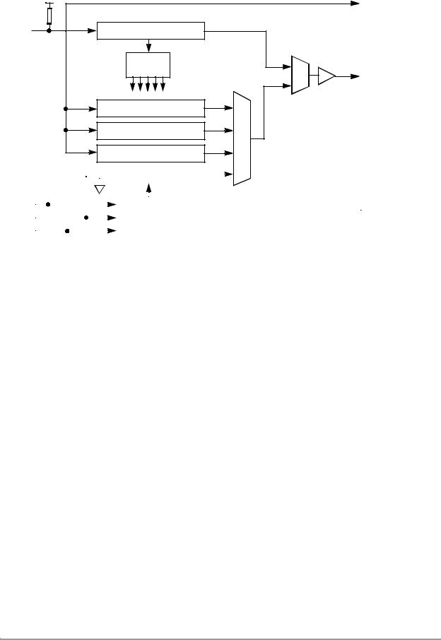
Figure 13-1. JTAG Block Diagram |
|
||||
A block diagram of the JTAG port is shown in Figure 13-1. The JTAG port has four read/write registers: the IR, BSR, device identification register, and bypass register. Access to the OnCE registers is described in Chapter 12, “OnCE™ Module.”
The TAP controller provides access to the JTAG IR through the JTAG port. The other JTAG registers must be individually selected by the JTAG IR. Figure 13-2 shows the programming models for the JTAG registers on the DSP56824.
JTAG Port 13-3
For More Information On This Product,
Go to: www.freescale.com