
- •List of Figures
- •List of Tables
- •List of Examples
- •About This Book
- •1.1 DSP56824 Architecture Overview
- •1.1.1 DSP56824 Peripheral Blocks
- •1.1.1.1 On-Chip Memory
- •1.1.1.2 External Memory Interface (Port A)
- •1.1.1.3 General-Purpose Input/Output Port (Port B)
- •1.1.1.4 Programmable I/O Port (Port C)
- •1.1.1.5 Serial Peripheral Interface (SPI)
- •1.1.1.6 Synchronous Serial Interface (SSI)
- •1.1.1.7 General-Purpose Timer Module
- •1.1.1.8 On-Chip Clock Synthesis Block
- •1.1.1.9 COP/RTI Module
- •1.1.1.10 JTAG/OnCE™ Port
- •1.1.2 DSP56824 Peripheral Interrupts
- •1.2 DSP56800 Core Description
- •1.2.1 Data Arithmetic Logic Unit (Data ALU)
- •1.2.2 Address Generation Unit (AGU)
- •1.2.3 Program Controller and Hardware Looping Unit
- •1.2.4 Bit-Manipulation Unit
- •1.2.5 Address and Data Buses
- •1.2.6 On-Chip Emulation (OnCE) Module
- •1.3 DSP56800 Programming Model
- •1.4 Code Development on the DSP56824
- •2.1 Power and Ground Signals
- •2.2 Clock and Phase Lock Loop (PLL) Signals
- •2.3 External Memory Interface (Port A)
- •2.4 Interrupt and Mode Control Signals
- •2.5 GPIO Signals
- •2.6 Serial Peripheral Interface (SPI) Signals
- •2.7 Synchronous Serial Interface (SSI) Signals
- •2.8 Timer Module Signals
- •2.9 JTAG/OnCE Port Signals
- •3.1 DSP56824 Memory Map
- •3.1.1 X Data Memory
- •3.1.2 Operating Mode Register (OMR)
- •3.1.2.1 Nested Looping (NL)—Bit 15
- •3.1.2.2 Reserved Bits—Bits 14–9
- •3.1.2.3 Condition Codes (CC)—Bit 8
- •3.1.2.4 Reserved Bit—Bit 7
- •3.1.2.5 Stop Delay (SD)—Bit 6
- •3.1.2.6 Rounding (R)—Bit 5
- •3.1.2.7 Saturation (SA)—Bit 4
- •3.1.2.8 External X Memory (EX)—Bit 3
- •3.1.2.9 Reserved Bit—Bit 2
- •3.1.3 DSP56824 Status Register (SR)
- •3.1.4 On-Chip Peripheral Memory Map
- •3.1.5 Program Memory Map
- •3.2 DSP56824 Operating Modes
- •3.2.1 Single Chip Bootstrap Mode (Mode 0)
- •3.2.2 Single Chip User (Mode 1)
- •3.2.3 Normal Expanded Mode (Mode 2)
- •3.2.4 Development Mode (Mode 3)
- •3.3 DSP56824 Reset and Interrupt Vectors
- •3.3.1 DSP56824 Interrupt Priority Register (IPR)
- •3.3.2 Interrupt Priority Structure
- •4.1 External Memory Port Architecture
- •4.2 Port A Description
- •4.2.1 Bus Control Register (BCR)
- •4.2.1.1 Reserved Bits—Bits 15–10
- •4.2.1.2 Drive (DRV)—Bit 9
- •4.2.1.3 Reserved Bit—Bit 8
- •4.2.2 Pins in Different Processing States
- •5.1 Port B Programming Model
- •5.1.1 Port B Data Direction Register (PBDDR)
- •5.1.2 Port B Data (PBD) Register
- •5.1.2.1 PBD Bit Values for General-Purpose Inputs
- •5.1.2.2 PBD Bit Values for General-Purpose Outputs
- •5.1.2.3 PBD Bit Values for Interrupt Inputs
- •5.1.3 Port B Interrupt (PBINT) Register
- •5.2 Port B Interrupt Generation
- •5.3 Port B Programming Examples
- •5.3.1 Receiving Data on Port B
- •5.3.2 Sending Data on Port B
- •5.3.3 Looping Data on Port B
- •5.3.4 Generating Interrupts on Port B
- •6.1 Port C Programming Model
- •6.1.1 Port C Control (PCC) Register
- •6.1.2 Port C Data Direction Register (PCDDR)
- •6.1.3 Port C Data (PCD) Register
- •6.2 Port C Programming Examples
- •6.2.1 Receiving Data on Port C GPIO Pins
- •6.2.2 Sending Data on Port C GPIO Pins
- •6.2.3 Looping Data on Port C GPIO Pins
- •7.1 SPI Architecture
- •7.2 SPI Programming Model
- •7.2.1 SPI Control Registers (SPCR0 and SPCR1)
- •7.2.1.1 Reserved Bits—Bits 15–9
- •7.2.1.2 SPI Clock Rate Select (SPR[2:0])—Bits 8, 1–0
- •7.2.1.3 SPI Interrupt Enable (SPIE)—Bit 7
- •7.2.1.4 SPI Enable (SPE)—Bit 6
- •7.2.1.5 Wired-OR Mode (WOM)—Bit 5
- •7.2.1.6 Master Mode Select (MST)—Bit 4
- •7.2.1.7 Clock Polarity (CPL)—Bit 3
- •7.2.1.8 Clock Phase (CPH)—Bit 2
- •7.2.2 SPI Status Register (SPSR0 and SPSR1)
- •7.2.2.1 Reserved Bits—Bits 15–8
- •7.2.2.2 SPI Interrupt Complete Flag (SPIF)—Bit 7
- •7.2.2.3 Write Collision (WCOL)—Bit 6
- •7.2.2.4 Reserved Bit—Bit 5
- •7.2.2.5 Mode Fault (MDF)—Bit 4
- •7.2.2.6 Reserved Bits—Bits 3–0
- •7.2.3 SPI Data Registers (SPDR0 and SPDR1)
- •7.3 SPI Data and Control Pins
- •7.4 SPI System Errors
- •7.4.1 SPI Mode-Fault Error
- •7.4.2 SPI Write-Collision Error
- •7.4.3 SPI Overrun
- •7.5 Configuring Port C for SPI Functionality
- •7.6 Programming Examples
- •7.6.1 Configuring an SPI Port as Master
- •7.6.2 Configuring an SPI Port as Slave
- •7.6.3 Sending Data from Master to Slave
- •8.1 SSI Architecture
- •8.1.1 SSI Clocking
- •8.1.2 SSI Clock and Frame Sync Generation
- •8.2 SSI Programming Model
- •8.2.1 SSI Transmit Shift Register (TXSR)
- •8.2.2 SSI Transmit Data Buffer Register
- •8.2.3 SSI Transmit Data (STX) Register
- •8.2.4 SSI Receive Shift Register (RXSR)
- •8.2.5 SSI Receive Data Buffer Register
- •8.2.6 SSI Receive Data (SRX) Register
- •8.2.7 SSI Transmit and Receive Control Registers
- •8.2.7.1 Prescaler Range (PSR)—Bit 15
- •8.2.7.2 Word Length Control (WL[1:0])—Bits 14–13
- •8.2.7.3 Frame Rate Divider Control (DC[4:0])—Bits 12–8
- •8.2.7.4 Prescale Modulus Select (PM[7:0])—Bits 7–0
- •8.2.8 SSI Control Register 2 (SCR2)
- •8.2.8.1 Receive Interrupt Enable (RIE)—Bit 15
- •8.2.8.2 Transmit Interrupt Enable (TIE)—Bit 14
- •8.2.8.3 Receive Enable (RE)—Bit 13
- •8.2.8.4 Transmit Enable (TE)—Bit 12
- •8.2.8.5 Receive Buffer Enable (RBF)—Bit 11
- •8.2.8.6 Transmit Buffer Enable (TBF)—Bit 10
- •8.2.8.7 Receive Direction (RXD)—Bit 9
- •8.2.8.8 Transmit Direction (TXD)—Bit 8
- •8.2.8.9 Synchronous Mode (SYN)—Bit 7
- •8.2.8.10 Transmit Shift Direction (TSHFD)—Bit 6
- •8.2.8.11 Transmit Clock Polarity (TSCKP)—Bit 5
- •8.2.8.12 SSI Enable (SSIEN)—Bit 4
- •8.2.8.13 Network Mode (NET)—Bit 3
- •8.2.8.14 Frame Sync Invert (FSI)—Bit 2
- •8.2.8.15 Frame Sync Length (FSL)—Bit 1
- •8.2.8.16 Early Frame Sync (EFS)—Bit 0
- •8.2.9 SSI Control/Status Register (SCSR)
- •8.2.9.1 Reserved Bit—Bit 15
- •8.2.9.2 Receive Shift Direction (RSHFD)—Bit 14
- •8.2.9.3 Receive Clock Polarity (RSCKP)—Bit 13
- •8.2.9.4 Reserved Bits—Bits 12–11
- •8.2.9.5 Receive Frame Sync Invert (RFSI)—Bit 10
- •8.2.9.6 Receive Frame Sync Length (RFSL)—Bit 9
- •8.2.9.7 Receive Early Frame Sync (REFS)—Bit 8
- •8.2.9.8 Receive Data Register Full (RDF)—Bit 7
- •8.2.9.9 Transmit Data Register Empty (TDE)—Bit 6
- •8.2.9.10 Receiver Overrun Error (ROE)—Bit 5
- •8.2.9.11 Transmitter Underrun Error (TUE)—Bit 4
- •8.2.9.12 Transmit Frame Sync (TFS)—Bit 3
- •8.2.9.13 Receive Frame Sync (RFS)—Bit 2
- •8.2.9.14 Receive Data Buffer Full (RDBF)—Bit 1
- •8.2.9.15 Transmit Data Buffer Empty (TDBE)—Bit 0
- •8.2.10 SSI Time Slot Register (STSR)
- •8.3 SSI Data and Control Pins
- •8.4 SSI Operating Modes
- •8.4.1 Normal Mode
- •8.4.1.1 Normal Mode Transmit
- •8.4.1.2 Normal Mode Receive
- •8.4.2 Network Mode
- •8.4.2.1 Network Mode Transmit
- •8.4.2.2 Network Mode Receive
- •8.4.3 Gated Clock Operation
- •8.5 SSI Reset and Initialization Procedure
- •8.6 Configuring Port C for SSI Functionality
- •9.1 Timer Programming Model
- •9.1.1 Timer Control Registers (TCR01 and TCR2)
- •9.1.1.1 Timer Enable (TE)—Bit 15, Bit 7
- •9.1.1.2 Invert (INV)—Bit 6
- •9.1.1.3 Overflow Interrupt Enable (OIE)—Bit 12, Bit 4
- •9.1.1.4 Timer Output Enable (TO[1:0])—Bits 11–10, Bits 3–2
- •9.1.1.5 Event Select (ES[1:0])—Bits 9–8, Bits 1–0
- •9.1.1.6 Reserved TCR Bits
- •9.1.2 Timer Preload Register (TPR)
- •9.1.3 Timer Count Register (TCT)
- •9.2 Timer Resolution
- •9.3 Timer Interrupt Priorities
- •9.4 Event Counting with the Timer Module
- •9.5 Timer Module Low-Power Operation
- •9.5.1 Turning Off the Entire Timer Module
- •9.5.2 Turning Off Any Timer Not in Use
- •9.5.3 Lowering the Timer Frequency
- •9.5.4 Running the Timer in Wait Mode
- •9.5.5 Running the Timer in Stop Mode
- •9.6 Timer Module Timing Diagrams
- •9.7 Configuring Port C for Timer Functionality
- •10.1 Timing System Architecture
- •10.1.1 Oscillator
- •10.1.2 Phase Lock Loop (PLL)
- •10.1.3 Prescaler
- •10.1.4 Clockout Multiplexer (MUX)
- •10.1.5 Control Registers
- •10.2 Clock Synthesis Programming Model
- •10.2.1 PLL Control Register 1 (PCR1)
- •10.2.1.1 Reserved Bit—Bit 15
- •10.2.1.2 PLL Enable (PLLE)—Bit 14
- •10.2.1.3 PLL Power Down (PLLD)—Bit 13
- •10.2.1.4 Low Power Stop (LPST)—Bit 12
- •10.2.1.5 Test Enable (TSTEN)—Bit 11
- •10.2.1.6 Prescaler Divider (PS[2:0])—Bits 10–8
- •10.2.1.7 CLKO Select (CS[1:0])—Bits 7–6
- •10.2.1.8 Reserved Bits—Bits 5–4
- •10.2.1.9 VCO Curve Select (VCS0)—Bit 3
- •10.2.1.10 Reserved Bits—Bits 2–0
- •10.2.2 PLL Control Register 0 (PCR0)
- •10.2.2.1 Reserved Bit—Bit 15
- •10.2.2.2 Feedback Divider (YD[9:0])—Bits 14–5
- •10.2.2.3 Reserved Bits—Bits 4–0
- •10.3 Low-Power Wait and Stop Modes
- •10.3.2 COP, Realtime Clock and CLKO Pin Enabled
- •10.3.3 PLL and CLKO Pin Enabled
- •10.3.4 CLKO Pin Enabled
- •10.3.5 Everything Disabled
- •10.4 PLL Lock
- •10.4.1 PLL Programming Example
- •10.4.2 Changing the PLL Frequency
- •10.4.3 Turning Off the PLL Before Entering Stop Mode
- •10.5 PLL Module Low-Power Operation
- •10.5.1 Turning Off the Entire Clock Synthesis Module
- •10.5.2 Turning Off the Prescaler Divider When Not in Use
- •10.5.3 Turning Off the PLL When Not in Use
- •10.5.4 Turning Off the CLKO Pin When Not in Use
- •11.1 COP and Real-Time Timer Architecture
- •11.2 COP and RTI Timer Programming Model
- •11.2.1 COP and RTI Control Register (COPCTL)
- •11.2.1.1 COP Enable (CPE)—Bit 15
- •11.2.1.2 COP Timer Divider (CT)—Bit 14
- •11.2.1.3 Reserved Bits—Bits 13–12
- •11.2.1.4 RTI Timer Enable (RTE)—Bit 11
- •11.2.1.5 RTI Enable (RTIE)—Bit 10
- •11.2.1.6 RTI Flag (RTIF)—Bit 9
- •11.2.1.7 RTI Prescaler (RP)—Bit 8
- •11.2.1.8 RTI/COP Divider (DV[7:0])—Bits 7–0
- •11.2.2 COP and RTI Count (COPCNT) Register
- •11.2.2.1 Reserved Bits—Bits 15–13
- •11.2.2.2 RTI/COP Divider (DV[7:0])—Bits 12–5
- •11.2.2.3 RTI Prescaler (RP[1:0])—Bits 4–3
- •11.2.2.4 Scaler (SC[2:0])—Bits 2–0
- •11.2.3 COP Reset (COPRST) Register
- •11.3 Programming the COP and RTI Timers
- •11.3.1 COP and RTI Timer Resolution
- •11.3.2 COP/RTI Timer Low-Power Operation
- •11.3.3 Programming Example
- •12.1 Combined JTAG/OnCE Interface Overview
- •12.2 JTAG/OnCE Port Pinout
- •12.3 OnCE Module Architecture
- •12.3.1 OnCE Port Block Diagram
- •12.3.2 OnCE Programming Model
- •12.3.3 OnCE State Machine and Control Block
- •12.4 Command, Status, and Control Registers
- •12.4.1 OnCE Shift Register (OSHR)
- •12.4.2 OnCE Command Register (OCMDR)
- •12.4.3 OnCE Decoder (ODEC)
- •12.4.4 OnCE Control Register (OCR)
- •12.4.4.1 COP Timer Disable (COPDIS)—Bit 15
- •12.4.4.2 DE Pin Output Enable (DE)—Bit 14
- •12.4.4.3 Breakpoint Configuration (BK[4:0])—Bits 13–9
- •12.4.4.4 Debug Request Mask (DRM)—Bit 8
- •12.4.4.5 FIFO Halt (FH)—Bit 7
- •12.4.4.6 Event Modifier (EM[1:0])—Bits 6–5
- •12.4.4.7 Power Down Mode (PWD)—Bit 4
- •12.4.4.8 Breakpoint Selection (BS[1:0])—Bits 3–2
- •12.4.4.9 Breakpoint Enable (BE[1:0])—Bits 1–0
- •12.4.5 OnCE Breakpoint 2 Control Register (OBCTL2)
- •12.4.5.1 Reserved OBCTL2 Register Bits
- •12.4.5.2 Enable (EN)—Bit 2
- •12.4.5.3 Invert (INV)—Bit 1
- •12.4.5.4 Data/Address Select (DAT)—Bit 0
- •12.4.6 OnCE Status Register (OSR)
- •12.4.6.1 Reserved OSR Bits—Bits 7–5
- •12.4.6.2 OnCE Core Status (OS[1:0])—Bits 4–3
- •12.4.6.3 Trace Occurrence (TO)—Bit 2
- •12.4.6.4 Hardware Breakpoint Occurrence (HBO)—Bit 1
- •12.4.6.5 Software Breakpoint Occurrence (SBO)—Bit 0
- •12.5 Breakpoint and Trace Registers
- •12.5.1 OnCE Breakpoint/Trace Counter Register (OCNTR)
- •12.5.2 OnCE Memory Address Latch (OMAL) Register
- •12.5.3 OnCE Breakpoint Address Register (OBAR)
- •12.5.4 OnCE Memory Address Comparator (OMAC)
- •12.5.5 OnCE Breakpoint and Trace Section
- •12.6 Pipeline Registers
- •12.6.1 OnCE PAB Fetch Register (OPABFR)
- •12.6.2 OnCE PAB Decode Register (OPABDR)
- •12.6.3 OnCE PAB Execute Register (OPABER)
- •12.6.4 OnCE PAB Change-of-Flow FIFO (OPFIFO)
- •12.6.5 OnCE PDB Register (OPDBR)
- •12.6.6 OnCE PGDB Register (OPGDBR)
- •12.6.7 OnCE FIFO History Buffer
- •12.7 Breakpoint 2 Architecture
- •12.8 Breakpoint Configuration
- •12.8.1 Programming the Breakpoints
- •12.8.2 OnCE Trace Logic Operation
- •12.9 The Debug Processing State
- •12.9.1 OnCE Normal, Debug, and Stop Modes
- •12.9.2 Entering Debug Mode
- •12.9.2.1 JTAG DEBUG_REQUEST and the Debug Event Pin
- •12.9.2.2 Software Request During Normal Activity
- •12.9.2.3 Trigger Events (Breakpoints and Trace Modes)
- •12.9.2.5 Exiting Debug Mode
- •12.10 Accessing the OnCE Module
- •12.10.1 Primitive JTAG Sequences
- •12.10.2 Entering the JTAG Test-Logic-Reset State
- •12.10.3 Loading the JTAG Instruction Register
- •12.10.4 Accessing a JTAG Data Register
- •12.10.4.1 JTAG/OnCE Interaction: Basic Sequences
- •12.10.4.2 Executing a OnCE Command by Reading the OCR
- •12.10.4.3 Executing a OnCE Command by Writing the OCNTR
- •12.10.4.4 OSR Status Polling
- •12.10.4.5 JTAG IR Status Polling
- •12.10.4.6 TRST/DE Pin Polling
- •12.10.5 Serial Protocol Description
- •12.10.5.1 Entering Debug Mode from User Mode
- •12.10.5.2 Entering Debug Mode from DSP Reset
- •12.10.5.3 Polling for OnCE Status
- •12.10.5.4 Setting Breakpoints in User Mode
- •12.10.5.5 Reading Pipeline Information in User Mode
- •12.10.5.6 Displaying a Specified Register
- •12.10.5.7 Displaying X Memory Area Starting at Address xxxx
- •12.10.5.8 Returning from Debug Mode to Normal Mode
- •12.10.5.9 Recovering from STOP or WAIT Execution
- •12.11 Using the OnCE Port
- •12.11.1 Beginning Debug Activity
- •12.11.2 Displaying a Specified Register
- •12.11.3 Displaying X Memory Area Starting at Address xxxx
- •12.11.4 Returning from Debug Mode to Normal Mode
- •12.12 OnCE Unit Low-Power Operation
- •13.1 JTAG/OnCE Port Pinout
- •13.2 JTAG Port Architecture
- •13.2.1 JTAG Instruction Register (IR) and Decoder
- •13.2.2 JTAG Chip Identification (CID) Register
- •13.2.3 JTAG Boundary Scan Register (BSR)
- •13.2.4 JTAG Bypass Register
- •13.3 TAP Controller
- •13.4 DSP56824 Restrictions
- •A.1 Design Considerations
- •A.1.1 Boot Source Selection
- •A.1.1.1 Bootstrapping from SPI0
- •A.1.1.2 Bootstrapping from Port A
- •A.1.2 COP Reset
- •A.1.3 No Load Option
- •A.2 Bootstrap Listing
- •B.1 DSP56824 BSDL Listing—100-Pin TQFP
- •C.1 Instruction Set Summary
- •C.2 Interrupt, Vector, and Address Tables
- •C.3 Programmer’s Sheets
- •Index

Chapter 11
COP and RTI Module
This section describes the Computer Operating Properly (COP) and real-time interrupt (RTI) module (COP/RTI) provided on the DSP56824.
The COP/RTI module provides two separate functions: a watchdog-like timer and a periodic interrupt generator. The COP timer guards processor activity and provides an automatic reset signal if a failure occurs. Both functions are contained in the same block because the input clock for both comes from a common clock divider.
11.1 COP and Real-Time Timer Architecture
The COP timer protects against system failures by providing a means to escape from unexpected input conditions, external events, or programming errors. Once started, the COP timer must be reset by software on a regular basis so that it never reaches its time-out value. When the COP timer reaches its time-out value, an internal reset is generated within the chip and the COP reset vector is fetched. It is assumed that if the COP reset is not received from the program, a system failure has occurred.
The COP functionality is typically used by software to ensure that the chip is operating properly. Software must periodically service the COP timer by correctly writing to the COP reset (COPRST) register before the COP timer times out. The COP timer has its own reset vector. This allows the reset recovery from a COP time-out to differ from the reset procedure done after a hardware reset.
A COP reset is very similar to a hardware reset through the RESET pin. The minor differences are the address from which the reset vector is fetched and the length of the period during which reset is asserted.
The RTI capability provides a periodic interrupt in an application. It consists of a long decrementing counter chain that runs continuously when enabled. When it reaches zero, a status flag is set and an interrupt is generated (optionally, when enabled by the user). The RTI has its own interrupt vector location to reduce overhead in interrupt servicing.
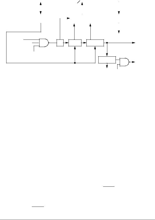
Figure 11-1 on page 11-2 shows a block diagram of the COP/RTI timer module. This module contains a programmable divider chain for dividing the prescaler clock to a periodic rate that can be used as an RTI. This real-time clock is further divided down to get a COP timer reset. The COP and RTI control (COPCTL) register is used to set up the peripheral and program the divide ratios.
COP and RTI Module |
11-1 |

COP and RTI Module
Peripheral Data Bus (PGDB) |
16-Bit |
|
|
|
|
|||||||
|
|
|
|
|
|
|
|
|
|
|
|
|
|
|
COPCTL |
|
|
|
COPCNT |
|
|
COPRST |
|||
|
|
|
|
|
|
|
||||||
|
|
|
||||||||||
|
|
|
|
|
|
|
|
|
|
|
|
|
|
16-Bit |
|
|
|
13-Bit |
|
16-Bit |
|
||||
|
Control Register |
|
|
|
Count Register |
|
$5 Detect |
|
||||
|
|
|
|
|
|
|
|
|
|
|
|
|
|
|
|
|
|
|
|
|
|
|
|
|
|
|
|
SC[2:0] |
RP[1:0] |
DV[7:0] |
|
|
Prescaler |
|
|
|
|
|
|
Clock |
RTE |
/23 |
/1 or /4 |
|
/2 to /256 |
Real-Time |
|
|
Interrupt |
||||
|
|
|
|
|
|
|
|
OnCE |
RP |
DV[7:0] |
|
||
|
Disable |
|
||||
|
|
|
|
/8 or /64 |
COP |
|
|
|
|
|
|
||
|
|
|
|
|
|
Reset |
CT |
CPE |
AA1386 |
Figure 11-1. RTI and COP Timer Block Diagram
NOTE:
The maximum frequency of the prescaler clock is limited to one-sixteenth of the maximum clocking frequency of the part. This means that for a 70 MHz DSP56824, the clocking frequency of the prescaler clock must be less than or equal to 4.375 MHz.
The RTI timer and the COP timer share the scaler (SC), real-time prescaler (RP), and COP/RTI divider (DV) dividers in the clock divider chain. The current value of the RTI timer can be determined at any time by reading the COP/RTI count (COPCNT) register, the bits of which reflect the shared components of the COP/RTI divider chain. These shared components comprise the RTI timer.
The COP timer is a timer whose clock source is cascaded from the RTI timer. It consists of the COP timer (CT) divider. The COP timer counts from either 7 or 63 down to 0, and then provides the COP reset signal, which resets the DSP chip. The COP timer cannot be read. Its only function is to count down to 0 and send a COP reset signal, unless the COP timer itself is reset. The COP reset sequence, provided in Example 11-1 on page 11-9, must be programmed to run periodically. Sending this reset sequence is analogous to renewing a library book before it is due.
The COPCTL register reflects the control status of both the RTI timer and the COP timer. The COP/RTI peripheral is enabled by the RTI enable (RTE) bit in the COPCTL register. In addition, the On-Chip Emulation (OnCE™ ) module within the DSP56800 core can disable the counting in the RTI and COP timers to prevent counting when the chip is no longer executing instructions, but instead is in debug mode. This is useful for debugging real-time systems.
When the COP timer expires and a COP reset occurs, the following sequence takes place:
1.DSP reset occurs.
2.The original MODA and MODB values that were captured on RESET deassertion are reloaded into the MA and MB bits of the OMR.
3.Program control is transferred to the appropriate COP reset vector determined by the values in MA and MB.
MODA, MODB, and XCOLF are not resampled on COP reset.
11-2 |
DSP56824 User’s Manual |
|