


DSP56824 Overview
1.4 Code Development on the DSP56824
The DSP56824 instruction set, described in detail in the DSP56800 Family Manual, provides assembly-level programming for this product. This manual provides a number of samples of source code to demonstrate the programming of certain features. These examples are not comprehensive; they are only a sampling of what is possible. See the DSP56800 Family Manual for more information on development hardware and software products for the DSP56824, including an Application Development System (ADS) that allows access to most DSP56824 functions and peripherals.
Two mechanisms on the DSP56824 aid code development—full access by all instructions to the external data bus and OnCE module hooks. The first is useful when code is first being developed on a hardware platform using external program memory. This section describes this first option. The OnCE module is fully described in Chapter 12, “OnCE™ Module.”
Instructions on the DSP56824 can be executed without regard for whether the instruction fetch is on-chip or off-chip and whether any data access is on-chip or off-chip. However, executing an instruction (including parallel moves) may require as many as three memory accesses. If more than one of these memory accesses occurs off-chip, an additional instruction cycle is required for every external access because only one access to external memory can occur at a time. This is shown in Example 1-1 and in the following discussion.
Example 1-1. On-Chip and Off-Chip Instruction Fetches
mac x0,y0,a x:(r0)+,y0 x:(r3)+,x0
The various permutations of memory accesses that may be represented in Example 1-1 are:
•Case 1—Instruction located on-chip, both x:() data accesses performed to on-chip memory
In this case, because all memories are located on-chip, no external accesses are performed and the instruction runs in one instruction cycle, correctly performing all three accesses to on-chip memory.
•Case 2—Instruction located off-chip, both x:() data accesses performed to on-chip memory
In this case, only one external memory access occurs off-chip. The instruction fetch occurs over the external bus, and the data accesses are made to on-chip memory. The instruction still runs in one instruction cycle, correctly performing all three accesses.
•Case 3—Instruction located on-chip, one x:() data access performed to off-chip memory
In this case, only one external memory access occurs off-chip. The instruction fetch is done to on-chip memory, one data access occurs over the external bus, and one data access is done to on-chip memory. The instruction still runs in one instruction cycle, correctly performing all three accesses.
•Case 4—Instruction located off-chip, one x:() data access performed to off-chip memory
In this case, two external memory accesses occur off-chip. The instruction fetch occurs over the external bus, followed by the external data access. A data access to internal memory also takes place. The instruction now runs in two instruction cycles, correctly performing all three accesses.
Case 4 is often used during code development to provide the best visibility. This feature allows a logic analyzer to be placed on the external bus during code development on target hardware so that all memory accesses are visible. Separate PS and DS pins are provided to indicate whether the access is to external program or data memory.
1-12 |
DSP56824 User’s Manual |
|
Code Development on the DSP56824
NOTE:
In this mode, accesses to on-chip peripherals are not visible because these memory-mapped registers are on-chip.
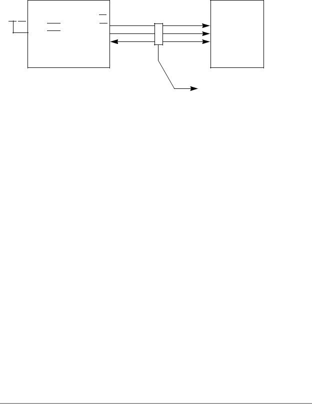
An example of a system where all program and memory accesses are visible is shown in Figure 1-5.
DSP56824
 MODA/IRQA
MODB/IRQB
64K SRAM
PS |
|
DS |
A15 |
ADR |
A14–A0 |
DATA |
DATA |
To Logic Analyzer |
AA0127 |
Figure 1-5. Code Development with Visibility on All Memory Accesses
In this example, the DSP56824 is programmed for operating mode 3 (development mode) in the operating mode register (OMR) to specify that all program accesses are performed externally. See Section 3.1, “DSP56824 Memory Map,” on page 3-1 for a detailed description of the OMR. Likewise, the EX bit (in the OMR) is set to specify that data accesses are performed externally. An exception to this is the second access on any instruction that performs two reads in a single instruction. In this case, the second read using the R3 pointer always occurs to on-chip memory. If this is an issue, the instruction performing two data memory reads can be replaced by two instructions, each performing one of the two data memory accesses.
DSP56824 Overview |
1-13 |

DSP56824 Overview
1-14 |
DSP56824 User’s Manual |
|
Chapter 2
Signal Descriptions
The input and output signals of the DSP56824 are organized into functional groups, as shown in Table 2-1 on page 2-2 and as illustrated in Figure 2-1. In Table 2-2 on page 2-3 through Table 2-14 on page 2-12, each row describes the signal or signals present on an individual pin. Note that some pins can carry more than one signal, depending on chip configuration.
|
|
|
|
DSP56824 |
|
|
|
|
|
|
Port B |
|
Port B GPIO |
|
|
|
|
Programmable |
8 |
|
|
|
|
|
|
||
|
|
9 |
|
Interrupts/GPIO |
PB0–PB7 |
|
|
VDD |
Power |
|
|||
|
VDDPLL |
9 |
Port |
Dedicated |
8 |
|
|
VSS |
|
PB8–PB14 |
|||
|
Ground |
GPIO |
XCOLF |
|||
|
VSSPLL |
|
PB15 |
|||
|
|
|
|
|
||
|
|
|
|
|
|
Port C GPIO |
|
EXTAL |
|
|
Port C |
MISO0 |
PC0 |
|
|
|
SPI0 Port/ |
MOSI0 |
PC1 |
|
|
XTAL |
|
PLL and |
|||
|
|
SCK0 |
PC2 |
|||
|
|
GPIO |
||||
|
CLKO |
|
Clock |
|||
|
|
SS0 |
PC3 |
|||
|
|
|
||||
|
SXFC |
|
|
|
||
|
|
|
|
|
|
|
|
|
|
|
SPI1 Port/ |
MISO1 |
PC4 |
|
|
|
Port A |
MOSI1 |
PC5 |
|
|
|
|
GPIO |
|||
|
|
16 |
External |
SCK1 |
PC6 |
|
|
|
|
||||
|
A0–A15 |
|
SS1 |
PC7 |
||
|
|
Address |
|
|||
|
|
|
Bus |
|
STD |
PC8 |
|
|
|
|
|
||
|
D0–D15 |
16 |
External |
SSI Port/ |
SRD |
PC9 |
|
|
Data |
GPIO |
STCK |
PC10 |
|
|
|
|
Bus |
|
STFS |
PC11 |
|
PS |
|
|
|
SRCK |
PC12 |
|
|
External |
|
SRFS |
PC13 |
|
|
DS |
|
|
|
|
|
|
|
Bus |
Timer Module/ |
|
|
|
|
RD |
|
TIO01 |
PC14 |
||
|
|
Control |
GPIO |
|||
|
WR |
|
TIO2 |
PC15 |
||
|
|
|
|
|||
After |
During |
|
|
|
TCK |
|
Reset |
Reset |
|
|
JTAG/ |
|
|
|
|
TMS |
|
|||
IRQA |
MODA |
|
Interrupt/ |
|
||
|
OnCE |
TDI |
|
|||
IRQB |
MODB |
|
Mode |
|
||
|
Port |
TDO |
|
|||
RESET |
RESET |
|
Control |
|
||
|
|
TRST/DE |
|
|||
|
|
|
|
|
AA1431 |
|
|
|
|
|
|
|
|
|
Figure 2-1. DSP56824 Functional Group Pin Allocations |
|
||||
Signal Descriptions |
2-1 |

Signal Descriptions
The interface signals have the following general characteristics:
•The following pins are pulled high with a weak on-chip resistor: TDI, TMS, and TRST/DE.
•The following pins are pulled high by the DSP during hardware reset (assertion of RESET): PS, DS, RD, WR, and XCOLF/PB15.
•The following pins can be pulled high by the DSP during the JTAG EXTEST_PULLUP instruction: EXTAL, D0–D15, PB0–PB15, PC0–PC15, MODA/IRQA, MODB/IRQB, and RESET.
•All unused port pins configured as inputs should be properly terminated through a pull-up resistor except for pins that are tied to an internal pull-up or pull-down resistor. All power and ground pins should be connected to the appropriate low-impedance power and ground paths.
The I/O signals are organized into the functional groups, as summarized in Table 2-1.
Table 2-1. Functional Group Pin Allocations
Functional Group |
Number of |
Detailed Description |
|
Pins |
|||
|
|
||
|
|
|
|
|
|
|
|
Power (VDD or VDDPLL) |
10 |
Table 2-2 on page 2-3 |
|
|
|
|
|
Ground (VSS or VSSPLL) |
10 |
Table 2-3 on page 2-3 |
|
|
|
|
|
Clock and phase lock loop (PLL) |
4 |
Table 2-4 on page 2-3 |
|
|
|
|
|
Address bus |
16 |
Table 2-5 on page 2-4 |
|
|
|
|
|
Data bus |
16 |
Table 2-6 on page 2-4 |
|
|
|
|
|
Bus control |
4 |
Table 2-7 on page 2-4 |
|
|
|
|
|
Interrupt and mode control |
3 |
Table 2-8 on page 2-5 |
|
|
|
|
|
Programmable interrupt general-purpose input/output |
8 |
Table 2-9 on page 2-6 |
|
|
|
|
|
Dedicated general-purpose input/output |
8 |
Table 2-10 on page 2-7 |
|
|
|
|
|
Serial peripheral interface (SPI) ports * |
8 |
Table 2-11 on page 2-7 |
|
|
|
|
|
Synchronous serial interface (SSI) port * |
6 |
Table 2-12 on page 2-10 |
|
|
|
|
|
Timer module* |
2 |
Table 2-13 on page 2-11 |
|
|
|
|
|
JTAG/OnCE |
5 |
Table 2-14 on page 2-12 |
|
|
|
|
|
Note: *Alternately, general-purpose I/O pins |
|
|
|
|
|
|
2-2 |
DSP56824 User’s Manual |
|