


Synchronous Serial Interface
Table 8-7. SSI Control Bits Requiring Reset Before Change
Control Register |
Bit |
|
|
|
|
SCRRX |
WL0 |
SCRTX |
WL1 |
|
|
SCR2 |
TEFS |
|
TFSI |
|
TFSL |
|
NET |
|
RBF |
|
RXD |
|
TSCKP |
|
TSHFD |
|
SYN |
|
TBF |
|
TXN |
|
|
SCSR |
REFS |
|
RFSI |
|
RFSL |
|
RSCKP |
|
RSHFD |
|
|
NOTE:
The SSI bit clock must go low for at least one complete period to ensure proper SSI reset.
8.6 Configuring Port C for SSI Functionality
The Port C control (PCC) register is used to individually configure each pin as either an SSI pin or a GPIO pin. Setting the corresponding CC bit in the PCC register configures the pin as an SSI pin. When the PCC register bit is set, it is not necessary to program the corresponding PCDDR bit. The SSI peripheral ensures the correct direction of this pin. Programming the Port C data direction register (PCDDR) is necessary only when a pin is programmed as a GPIO pin.
8-30 |
DSP56824 User’s Manual |
|

Chapter 9
Timers
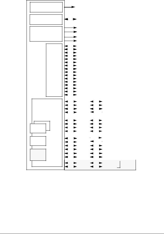
This section describes the timer module provided on the DSP56824 as a part of Port C. The timer module provides three independently programmable 16-bit timer/event counters, which are referred to as Timer 0, Timer 1, and Timer 2. All three timer/event counters can be clocked with signals coming from one of two internal sources. Timer 1 and Timer 2 can also be clocked by the overflow events of Timer 0 and Timer 1, respectively. In addition, when configured as inputs, the counters can be clocked with external signals from the timer I/O pins (TIO01 or TIO2) on Port C to count external events. The same pins, when configured as outputs, can be used to provide a timer pulse or for timer clock generation. The timer/event counters can be used either to interrupt the DSP56824 or to signal an external device at periodic intervals.
The capabilities of the timer module include the ability to do the following:
•Decrement a timer to zero and interrupt
•Decrement a timer to zero and apply a pulse to a TIO pin
•Decrement a timer to zero and toggle a TIO pin (50 percent duty cycle)
•Generate a wave form on a TIO pin with a duty cycle other than 50 percent using two timers
•Count events on an external TIO pin when selected as the input clock
•Operate timers independently or cascade timers together
Each timer can be clocked from the following:
•A TIO pin
•A clock running at half the instruction rate of the chip
•A slow clock generated from the prescaler divider
In addition, Timer 1 can be clocked by the overflow events of Timer 0, and Timer 2 can be clocked by the overflow events of Timer 1.
When a timer is clocked using the slower clock from the prescaler divider, it can continue counting even when the DSP56800 core is in stop mode. All three timers are capable of operating in stop mode. However, only Timer 2 is capable of bringing the DSP56800 core out of stop mode when it times out. Figure 9-1 on page 9-2 shows the timers provided on Port C, and Figure 9-2 on page 9-3 shows a block diagram of the timer module.
Timers 9-1
Timers
External
Address MUX
External
Data Switch
Bus Control
General-
Purpose
I/O
Peripheral
Communications
Interfaces
SPI (x2)
SSI
Timers
|
|
|
|
|
Default |
|
|
Alternate |
|
|
|||||||||||
|
|
|
|
|
Function |
|
|
Function |
|
|
|||||||||||
|
|
|
|
|
A15–A0 |
|
|
|
|
|
|||||||||||
|
|
|
|
|
D15–D0 |
|
|
|
|
|
|||||||||||
|
|
|
|
|
|
|
|
|
|||||||||||||
|
|
|
|
|
|
|
|
|
|
|
|
|
|
|
|
|
|
|
|
||
|
|
|
|
|
RD |
|
|
|
|
|
|
|
|
|
|
|
|
|
|
||
|
|
|
|
|
|
|
|
|
|
|
|
|
|
|
|
|
|
|
|||
|
|
|
|
|
WR |
|
|
|
|
|
|
|
|
|
|
|
|
|
|||
|
|
|
|
|
|
|
|
|
|
|
|
|
|
|
|||||||
|
|
|
|
|
PS |
|
|
|
|
|
|
|
|
|
|
||||||
|
|
|
|
|
DS |
|
|
|
|
|
|||||||||||
|
|
|
|
|
PB0 |
|
|
|
|
|
|||||||||||
|
|
|
|
|
|
|
|
|
|
||||||||||||
|
|
|
|
|
PB1 |
|
|
|
|
|
|||||||||||
|
|
|
|
|
|
|
|
|
|
||||||||||||
|
|
|
|
|
PB2 |
|
|
|
|
|
|||||||||||
|
|
|
|
|
|
|
|
|
|
||||||||||||
|
|
|
|
|
PB3 |
|
|
|
|
|
|||||||||||
|
|
|
|
|
|
|
|
|
|
||||||||||||
|
|
|
|
|
PB4 |
|
|
|
|
|
|||||||||||
|
|
|
|
|
|
|
|
|
|
||||||||||||
|
|
|
|
|
PB5 |
|
|
|
|
|
|||||||||||
|
|
|
|
|
|
|
|
|
|
||||||||||||
|
|
|
|
|
PB6 |
|
|
|
|
|
|||||||||||
|
|
|
|
|
|
|
|
|
|
||||||||||||
|
|
|
|
|
PB7 |
|
|
|
|
|
|||||||||||
|
|
|
|
|
|
|
|
|
|
||||||||||||
|
|
|
|
|
PB8 |
|
|
|
|
|
|||||||||||
|
|
|
|
|
|
|
|
|
|
||||||||||||
|
|
|
|
|
PB9 |
|
|
|
|
|
|||||||||||
|
|
|
|
|
|
|
|
|
|
||||||||||||
|
|
|
|
|
PB10 |
|
|
|
|
|
|||||||||||
|
|
|
|
|
|
|
|
|
|
||||||||||||
|
|
|
|
|
PB11 |
|
|
|
|
|
|||||||||||
|
|
|
|
|
|
|
|
|
|
||||||||||||
|
|
|
|
|
PB12 |
|
|
|
|
|
|||||||||||
|
|
|
|
|
|
|
|
|
|
||||||||||||
|
|
|
|
|
PB13 |
|
|
|
|
|
|||||||||||
|
|
|
|
|
|
|
|
|
|
||||||||||||
|
|
|
|
|
PB14 |
|
|
|
|
|
|||||||||||
|
|
|
|
|
|
|
|
|
|
||||||||||||
|
|
|
|
|
XCOLF |
/PB15 |
|
|
|
|
|
||||||||||
|
|
|
|
|
|
|
|
|
|
||||||||||||
|
|
|
|
|
PC0 |
|
|
|
|
|
|
|
MISO0 |
|
|
||||||
|
|
|
|
|
|
|
|
|
|
|
|
||||||||||
|
|
|
|
|
PC1 |
|
|
|
|
|
|
|
MOSI0 |
|
|
||||||
|
|
|
|
|
|
|
|
|
|
|
|
||||||||||
|
|
|
|
|
PC2 |
|
|
|
|
|
|
|
SCK0 |
|
|
||||||
|
|
|
|
|
|
|
|
|
|
|
|
||||||||||
|
|
|
|
|
PC3 |
|
|
|
|
|
SS0 |
|
|
||||||||
|
|
|
|
|
|
|
|
|
|
|
|||||||||||
|
|
|
|
PC4 |
|
|
|
|
|
|
|
MISO1 |
|
|
|||||||
|
|
|
|
|
|
|
|
|
|
||||||||||||
|
|
|
|
PC5 |
|
|
|
|
|
|
|
MOSI1 |
|
|
|||||||
|
|
|
|
|
|
|
|
|
|
||||||||||||
|
|
|
|
PC6 |
|
|
|
|
|
|
|
SCK1 |
|
|
|||||||
|
|
|
|
|
|
|
|
|
|
||||||||||||
|
|
|
|
PC7 |
|
|
|
|
|
|
|
SS1 |
|
|
|||||||
|
|
|
|
|
|
|
|
|
|
||||||||||||
|
|
|
|
|
PC8 |
|
|
|
|
STD |
|
|
|||||||||
|
|
|
|
|
|
|
|
|
|
||||||||||||
|
|
|
|
|
|
|
|||||||||||||||
|
|
|
|
|
PC9 |
|
|
|
|
SRD |
|
|
|||||||||
|
|
|
|
|
|
|
|
|
|
|
|||||||||||
|
|
|
|
|
|
|
|||||||||||||||
|
|
|
|
|
PC10 |
|
|
|
|
|
|
|
STCK |
|
|
||||||
|
|
|
|
|
|
|
|
|
|
|
|
||||||||||
|
|
|
|
|
PC11 |
|
|
|
|
|
|
|
STFS |
|
|
||||||
|
|
|
|
|
|
|
|
|
|
|
|
||||||||||
|
|
|
|
|
PC12 |
|
|
|
|
|
|
|
SRCK |
|
|
||||||
|
|
|
|
|
|
|
|
|
|
|
|
||||||||||
|
|
|
|
|
PC13 |
|
|
|
|
|
|
|
SRFS |
|
|
||||||
|
|
|
|
|
|
|
|
|
|
|
|
||||||||||
|
|
|
|
|
|
|
|
|
|
|
|
|
|
|
|
|
|
|
|
|
|
|
|
|
|
|
PC14 |
|
|
|
|
|
|
|
TIO01 |
|
Timers |
||||||
|
|
|
|
|
|
|
|
|
|
|
|
|
|||||||||
|
|
|
|
|
|
|
|
|
|
||||||||||||
|
|
|
|
|
PC15 |
|
|
|
|
|
|
|
TIO2 |
|
|||||||
|
|
|
|
|
|
|
|
|
|
|
|
|
|
||||||||
AA1235
Figure 9-1. DSP56824 Input/Output Block Diagram
9-2 |
DSP56824 User’s Manual |
|