


SSI Data and Control Pins
8.3 SSI Data and Control Pins
The SSI has the following six dedicated I/O pins:
•Serial transmit data (STD/PC8)
•Serial receive data (SRD/PC9)
•Serial transmit clock (STCK/PC10)
•Serial transmit frame sync (STFS/PC11)
•Serial receive clock (SRCK/PC12)
•Serial receive frame sync (SRFS/PC13)
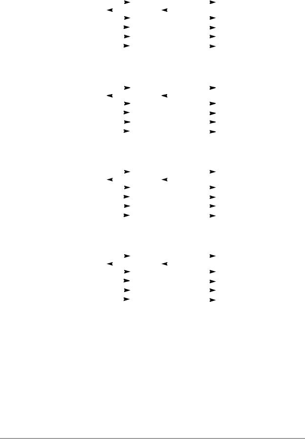
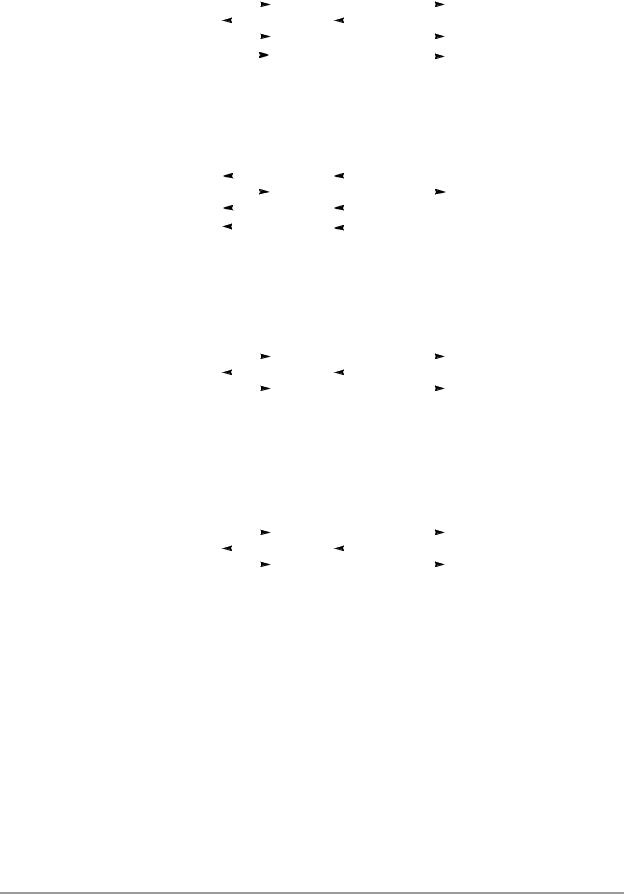
Figure 8-9 on page 8-20 and Figure 8-10 on page 8-21 show the main SSI configurations. These pins support all transmit and receive functions with a continuous or gated clock, as shown. Note that gated clock implementations do not require the use of the frame sync pins (STFS and SRFS). In this case, these pins can be used as GPIO pins, if desired.
Synchronous Serial Interface |
8-19 |
Synchronous Serial Interface
|
|
|
|
|
|
|
|
|
|
|
|
|
PC8 |
|
|
|
|
STD |
|
|
|
|
|
|
|
|
|
|
|||||||
|
PC9 |
|
|
|
|
SRD |
|
|
Any |
||
|
|
|
|
|
|
||||||
|
PC10 |
|
|
|
|
STCK |
|
|
|
|
|
DSP56824 |
|
|
|
|
|
|
|
DSP or |
|||
PC11 |
|
|
|
|
STFS |
|
|
|
|
||
|
|
|
|
|
|
|
|
codec |
|||
|
PC12 |
|
|
|
|
SRCK |
|
|
|
|
|
|
|
|
|
|
|
|
|
||||
|
PC13 |
|
|
|
|
SRFS |
|
|
|
||
|
|
|
|
|
|
|
|||||
|
|
|
|
|
|
|
|
|
|
||
|
SSI Internal Continuous Clock (Asynchronous) |
||||||||||
|
|
|
|
|
|
||||||
|
PC8 |
|
|
|
|
STD |
|
|
|
|
|
|
|
|
|
|
|||||||
|
PC9 |
|
|
|
|
SRD |
|
Any |
|||
|
|
|
|
|
|||||||
|
PC10 |
|
|
|
|
STCK |
|
|
|
|
|
DSP56824 |
|
|
|
|
|
|
DSP or |
||||
PC11 |
|
|
|
|
STFS |
|
|
|
|
||
|
|
|
|
|
|
|
codec |
||||
|
PC12 |
|
|
|
|
SRCK |
|
|
|
|
|
|
|
|
|
|
|
|
|
||||
|
PC13 |
|
|
|
|
SRFS |
|
|
|
||
|
|
|
|
|
|
|
|||||
|
|
|
|
||||||||
|
SSI External Continuous Clock (Asynchronous) |
||||||||||
|
|
|
|
|
|
||||||
|
|
|
|
|
|
|
|
|
|
|
|
|
PC8 |
|
|
|
|
STD |
|
|
|
|
|
|
|
|
|
|
|||||||
|
PC9 |
|
|
|
|
SRD |
|
Any |
|||
|
|
|
|
|
|||||||
|
PC10 |
|
|
|
|
STCK |
|
|
|
|
|
DSP56824 |
|
|
|
|
|
|
DSP or |
||||
PC11 |
|
|
|
|
STFS |
|
|
|
|
||
|
|
|
|
|
|
|
codec |
||||
|
PC12 |
|
|
|
|
SRCK |
|
|
|
|
|
|
|
|
|
|
|
|
|
||||
|
PC13 |
|
|
|
|
SRFS |
|
|
|
||
|
|
|
|
|
|
|
|||||
|
|
|
|
||||||||
|
SSI Continuous Clock (RX = Internal, TX = External, Asynchronous) |
||||||||||
|
|
|
|
|
|
||||||
|
PC8 |
|
|
|
|
STD |
|
|
|
|
|
|
|
|
|
|
|||||||
|
PC9 |
|
|
|
|
SRD |
|
Any |
|||
|
|
|
|
|
|||||||
|
PC10 |
|
|
|
|
STCK |
|
|
|
|
|
DSP56824 |
|
|
|
|
|
|
DSP or |
||||
PC11 |
|
|
|
|
STFS |
|
|
|
|
||
|
|
|
|
|
|
|
codec |
||||
|
PC12 |
|
|
|
|
SRCK |
|
|
|
|
|
|
|
|
|
|
|
|
|
||||
|
PC13 |
|
|
|
|
SRFS |
|
|
|
||
|
|
|
|
|
|
|
|||||
|
|
|
|
|
|
|
|
|
|
|
|
SSI Continuous Clock (RX = External, TX = Internal, Asynchronous) |
AA1438 |
|
Figure 8-9. Asynchronous SSI Configurations—Continuous Clock
8-20 |
DSP56824 User’s Manual |
|
|
|
|
|
|
|
|
|
|
|
|
SSI Data and Control Pins |
|
|
|
|
|
|
|
|
|
|
||||
|
PC8 |
|
|
|
|
|
STD |
|
|
|
|
|
|
|
|
|
|
|
|
||||||
|
PC9 |
|
|
|
|
|
SRD |
|
Any |
|
||
|
|
|
|
|
|
|||||||
|
PC10 |
|
|
|
|
|
STCK |
|
|
|
|
|
DSP56824 |
|
|
|
|
|
|
|
DSP or |
|
|||
PC11 |
|
|
|
|
|
STFS |
|
|
|
|
||
|
|
|
|
|
|
|
|
codec |
|
|||
|
PC12 |
|
|
|
|
|
|
|
|
|
|
|
|
|
|
|
|
|
|
|
|
|
|
|
|
|
PC13 |
|
|
|
|
|
|
|
|
|
|
|
|
|
|
|
|
|
|
||||||
|
SSI Internal Continuous Clock (Synchronous) |
|
|
|||||||||
|
|
|
|
|
|
|
|
|
||||
|
PC8 |
|
|
|
|
|
STD |
|
|
|
|
|
|
|
|
|
|
|
|
|
|||||
|
PC9 |
|
|
|
|
|
SRD |
|
|
Any |
|
|
|
|
|
|
|
|
|
|
|||||
|
PC10 |
|
|
|
|
|
STCK |
|
|
|
||
DSP56824 |
|
|
|
|
|
|
DSP or |
|
||||
PC11 |
|
|
|
|
|
STFS |
|
|
|
|||
|
|
|
|
|
|
|
codec |
|
||||
|
|
|
|
|
|
|
||||||
|
PC12 |
|
|
|
|
|
|
|
|
|
|
|
|
|
|
|
|
|
|
|
|
|
|
|
|
|
PC13 |
|
|
|
|
|
|
|
|
|
|
|
|
|
|
|
|
||||||||
|
SSI External Continuous Clock (Synchronous) |
|
|
|||||||||
|
|
|
|
|
|
|
|
|
|
|
|
|
|
PC8 |
|
|
|
|
|
STD |
|
|
|
|
|
|
|
|
|
|
|
|
||||||
|
PC9 |
|
|
|
|
|
SRD |
|
Any |
|
||
|
|
|
|
|
|
|||||||
|
|
|
|
|
|
|
|
|
|
|
|
|
DSP56824 |
PC10 |
|
|
|
|
|
STCK |
|
|
DSP or |
|
|
|
|
|
|
|||||||||
PC11 |
|
|
|
|
|
|
|
|
|
MCU with |
|
|
|
|
|
|
|
|
|
|
|
|
|
||
|
PC12 |
|
|
|
|
|
|
|
|
|
SPI |
|
|
PC13 |
|
|
|
|
|
|
|
|
|
|
|
|
|
|
|
|
|
|
|
|
|
|
||
|
SSI Internal Gated Clock (Synchronous) |
|
|
|||||||||
|
|
|
|
|
|
|
|
|
||||
|
PC8 |
|
|
|
|
|
STD |
|
|
|
|
|
|
|
|
|
|
|
|
||||||
|
PC9 |
|
|
|
|
|
SRD |
|
Any |
|
||
|
|
|
|
|
|
|||||||
|
|
|
|
|
|
|
|
|
|
|
|
|
DSP56824 |
PC10 |
|
|
|
|
|
STCK |
|
|
DSP or |
|
|
|
|
|
|
|||||||||
PC11 |
|
|
|
|
|
|
|
|
|
MCU with |
|
|
|
|
|
|
|
|
|
|
|
|
|
||
|
PC12 |
|
|
|
|
|
|
|
|
|
SPI |
|
|
PC13 |
|
|
|
|
|
|
|
|
|
|
|
|
|
|
|
|
|
|
|
|||||
|
SSI External Gated Clock (Synchronous) |
|
AA1439 |
|||||||||
|
|
|
|
|
|
|
|
|
|
|
|
|
Figure 8-10. Synchronous SSI Configurations—Continuous and Gated Clock
The following paragraphs describe the configuration of the SSI pins.
•STD/PC8 (serial transmit data)—The STD pin transmits data from the serial transmit shift register. The STD pin is an output pin when data is being transmitted and is tri-stated between data word transmissions and on the trailing edge of the bit clock after the last bit of a word is transmitted. Connect an external resistor to this pin to prevent the signal from floating when not being driven. (A floating pin may provide spurious edge transitions or may go into oscillation.) Since this pin is tri-stated, the external resistor can be either high or low, depending on the circuit designer’s choice.
•SRD/PC9 (serial receive data)—The SRD pin is used to bring serial data into the receive data shift register.
Synchronous Serial Interface |
8-21 |
Synchronous Serial Interface
•STCK/PC10 (serial transmit clock)—The STCK pin can be used as either an input or an output. This clock signal is used by the transmitter and can be either continuous or gated. During gated clock mode, data on the STCK pin is valid only during the transmission of data; otherwise it is tri-stated. In synchronous mode, this pin is used by both the transmit and receive sections. When gated clock mode is being used, an external resistor should be connected to this pin to prevent the signal from floating when not being driven.
•STFS/PC11 (serial transmit frame sync)—The STFS pin can be used as either an input or an output. The frame sync is used by the transmitter to synchronize the transfer of data. The frame sync signal can be 1 bit or 1 word in length and can occur 1 bit before the transfer of data or right at the transfer of data. In synchronous mode, this pin is used by both the transmit and receive sections. In gated clock mode, frame sync signals are not used.
•SRCK/PC12 (serial receive clock)—The SRCK pin can be used as either an input or an output. This clock signal is used by the receiver and is always continuous. During gated clock mode, the STCK pin is used instead for clocking in data. This pin is not used in synchronous mode.
•SRFS/PC13 (serial receive frame sync)—The SRFS pin can be used as either an input or an output. The frame sync is used by the receiver to synchronize the transfer of data. The frame sync signal can be 1 bit or 1 word in length and can occur 1 bit before the transfer of data or right at the transfer of data.
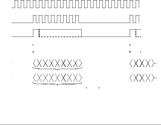
An example of the pin signals for an 8-bit data transfer is shown in Figure 8-11. Continuous and gated clock signals are shown, as well as the bit-length frame sync signal and the word-length frame sync signal. Note that the shift direction can be defined as MSB first or LSB first, and that there are other options on the clock and frame sync.
Continuous STCK, SRCK
Gated STCK, SRCK
STFS, SRFS
Early STFS, SRFS
|
|
|
|
|
|
|
|
|
|
|
|
|
|
|
|
|
|
|
|
|
|
|
|
|
|
|
|
|
|
|
|
|
|
|
|
|
|
|
|
|
|
|
|
|
|
|
|
|
|
|
|
|
|
|
|
|
|
|
|
|
|
|
|
|
|
|
|
|
|
|
|
|
|
|
|
|
|
|
|
|
|
|
|
|
|
|
|
|
|
|
|
|
|
|
|
|
|
|
|
|
|
|
|
|
|
|
|
|
|
|
|
|
|
|
|
|
|
|
|
|
|
|
|
|
|
|
|
|
|
|
|
|
|
|
|
|
|
|
|
|
|
|
|
|
|
|
|
|
|
|
|
|
|
|
|
|
|
|
|
|
|
|
|
|
|
|
|
|
|
|
|
|
|
|
|
|
|
|
|
|
|
|
|
|
|
|
|
|
|
|
|
|
|
|
|
|
|
|
|
|
|
|
|
|
|
|
|
|
|
|
|
|
|
|
|
|
|
|
|
|
|
|
|
|
|
|
|
|
|
|
|
|
|
|
|
|
|
|
|
|
|
|
|
|
|
|
|
|
|
|
|
|
|
|
|
|
|
|
|
|
|
|
|
|
|
|
|
|
|
|
|
|
|
|
|
|
|
|
|
|
|
|
|
|
|
|
|
|
|
|
|
|
|
|
|
|
|
|
|
|
|
|
|
|
|
|
|
|
|
|
|
|
|
|
|
|
|
|
|
|
|
|
|
|
|
|
|
|
|
|
|
|
|
|
|
|
|
|
|
|
|
|
|
|
|
|
|
|
|
|
|
|
|
|
|
|
|
|
|
STD |
|
|
|
|
|
|
|
|
|
|
|
|
|
|
|
|
|
|
|
|
|
|
|
|
|
|
|
|
|
|
|
|
|
|
|
|
|
|
|
|
|
|
|
|
|
|
|
|
|
|
|
|
|
|
|
|
|
|
|
|
|
|
|
|
|
|
|||||
|
|
|
|
|
|
|
|
|
|
|
|
|
|
|
|
|
|
|
|
|
|
|
|
|
|
|
|
|
|
|
|
|
|
|
|
|
|
|
|
|
|
|
|
|
|
|
|
|
|
|
|
|
|
|
|
|
|
|
|
|
|
|
|
|
|
||||||
|
|
|
|
7 |
6 |
5 |
|
4 |
3 |
|
|
|
|
2 |
1 |
0 |
|
|
|
|
|
|
|
|
|
|
|
|
7 |
|
|
|
|
6 |
|
|
5 |
|
4 |
||||||||||||||||||||||||||||||||
|
|
|
|
|
|
|
|
|
|
|
|
|
|||||||||||||||||||||||||||||||||||||||||||||||||||||||||||
|
|
|
|
|
|
|
|
|
|
|
|
|
|
|
|
|
|
|
|
|
|
|
|
|
|
|
|
|
|
|
|
|
|
|
|
|
|
|
|
|
|
|
|
|
|
|
|
|
|
|
|
|
|
|
|
|
|
|
|
|
|
|
|
|
|
|
|
|
|
||
SRD |
|
|
|
|
|
|
|
|
|
|
|
|
|
|
|
|
|
|
|
|
|
|
|
|
|
|
|
|
|
|
|
|
|
|
|
|
|
|
|
|
|
|
|
|
|
|
|
|
|
|
|
|
|
|
|
|
|
|
|
|
|
|
|
|
|
|
|||||
|
|
|
|
|
|
|
|
|
|
|
|
|
|
|
|
|
|
|
|
|
|
|
|
|
|
|
|
|
|
|
|
|
|
|
|
|
|
|
|
|
|
|
|
|
|
|
|
|
|
|
|
|
|
|
|
|
|
|
|
|
|
|
|
|
|
||||||
|
|
|
|
7 |
6 |
5 |
|
4 |
3 |
|
|
|
|
2 |
1 |
0 |
|
|
|
|
|
|
|
|
|
|
|
|
7 |
|
|
|
|
6 |
|
|
5 |
|
4 |
||||||||||||||||||||||||||||||||
|
|
|
|
|
|
|
|
|
|
|
|
|
|
|
|
|
|
|
|
|
|
|
|
|
|||||||||||||||||||||||||||||||||||||||||||||||
|
|
|
|
|
|
|
|
|
|
|
|
|
|
|
|
|
|
|
|
|
|
|
|
|
|
|
|
|
|
|
|
|
|
|
|
|
|
|
|
|
|
|
|
|
|
|
|
|
|
|
|
|
|
|
|
|
|
|
|
|
|
|
|
|
|
|
|
|
|
|
|
|
|
|
|
|
|
|
|
|
|
|
|
|
|
|
|
|
|
|
|
8-Bit Data |
|
|
|
|
|
|
|
|
|
|
|
|
|
|
|
|
|
|
|
|
|
Bit-Length Frame Sync |
|
|
|
|
|
|
|
||||||||||||||||||||||
|
|
|
|
|
|
|
|
|
|
|
|
|
|
|
|
|
|
|
|
|
|
|
|
|
|
|
|
|
|
|
|
|
|
|
|
|
|
|
|
|
|
|
|
|
|
|
|
||||||||||||||||||||||||
|
|
|
|
|
|
|
|
|
|
|
|
|
|
|
|
|
|
|
|
|
|
|
|
|
|
|
|
|
|
|
|
|
|
|
|
|
|
|
|
|
|
|
|
|
|
|
|
|
|
|
|
|
|
|
|
Word-Length Frame Sync |
|
|
|
||||||||||||
|
|
|
|
|
|
|
|
|
|
|
|
|
|
|
|
|
|
|
|
|
|
|
|
|
|
|
|
|
|
|
|
|
|
|
|
|
|
|
|
|
|
|
|
|
|
|
|
|
|
|
|
|
|
|
|
|
|
|
|||||||||||||
AA0155
Figure 8-11. Serial Clock and Frame Sync Timing
8-22 |
DSP56824 User’s Manual |
|