


Port C Programming Examples
6.2.3 Looping Data on Port C GPIO Pins
Example 6-3 shows how to configure Port C GPIO pins and then use them to loop data back from an output to an input.
Example 6-3. Loop-Back Example
;******************** |
|
|
|
;* LOOPBACK example * |
|
|
|
;* for Port C |
* |
|
|
;* of DSP56824 chip * |
|
|
|
;******************** |
|
|
|
START |
EQU |
$0040 |
; Start of program |
BCR |
EQU |
$FFF9 |
; Bus Control Register |
PCC |
EQU |
$FFED |
; Port C Control Register |
PCD |
EQU |
$FFEF |
; Port C Data |
PCDDR |
EQU |
$FFEE |
; Port C Data Direction Register |
data_o |
EQU |
$0000 |
; data output |
data_i |
EQU |
$0001 |
; data input |
;**************** |
|
|
|
;* Vector setup * |
|
|
|
;**************** |
|
|
|
ORG |
P:$0000 |
|
; Cold Boot |
JMP |
START |
|
; also Hardware RESET vector (Mode 0, 1, 3) |
ORG |
P:$E000 |
|
; Warm Boot |
JMP |
START |
|
; Hardware RESET vector (Mode 2) |
ORG |
P:START |
|
; Start of program |
;***************** |
|
|
|
;* General setup * |
|
|
|
;***************** |
|
|
|
MOVEP |
#$0000,X:BCR |
; External Program memory has 0 wait states. |
|
|
|
|
; External data memory has 0 wait states. |
|
|
|
; Port A pins are tri-stated when no |
;**************** |
|
; external access occurs. |
|
|
|
||
;* Port C setup * |
|
|
|
;**************** |
|
|
|
MOVEP |
#$0000,X:PCC |
; Configure PC0-PC15 as GPIO pins (default). |
|
MOVEP |
#$FF00,X:PCDDR |
; Select pins PC0-PC7 as input and |
|
;**************** |
|
; pins PC8-PC15 as output. |
|
|
|
||
;* Main routine * |
|
|
|
;**************** |
|
; ... |
|
LOOPBACK ; Test Loop |
|
||
|
|
||
MOVE |
X:data_o,X0 |
; Put bits 8-15 of “data_o” on pins PC8-PC15. |
|
MOVEP |
X0,X:PCD |
; Bits going to input pins are ignored. |
|
|
|
|
; ... |
MOVEP |
X:PCD,X0 |
; Read PC0-PC7 into bits 0-7 of “data_i”. |
|
MOVE |
X0,X:data_i |
; Bits 8-15 get values of PC8-PC15 as well. |
|
BRA |
LOOPBACK |
|
; ... |
|
|
||
|
|
|
|
Port C GPIO Functionality |
6-7 |

Port C GPIO Functionality
6-8 |
DSP56824 User’s Manual |
|

Chapter 7
Serial Peripheral Interface
This section discusses the architecture of the serial peripheral interface (SPI) provided on Port C, its pins, and its programming model. The section includes information on SPI system errors, a discussion of overrun on the SPI, correct programming of Port C when using the SPI, and low-power operation with the SPI.
The SPI is an independent, serial communications subsystem that allows the DSP56824 to communicate synchronously with peripheral devices such as LCD drivers, A/D subsystems, and microprocessors. More sophisticated uses, such as interprocessor communication in a multiple master system, are also easy to implement. The SPI can be configured as either a master or a slave device with high data rates. In Master mode, a transfer is initiated when data is written to the SPI data register (SPDR). In Slave mode, a transfer is initiated by the reception of a clock signal.
Clock control logic allows a selection of clock polarity and a choice of two fundamentally different clocking protocols to accommodate most available synchronous serial peripheral devices. In some cases, the phase and polarity are changed between transfers to allow a master device to communicate with peripheral slaves having different requirements. When the SPI is configured as a master, software selects one of eight different bit rates for the clock.
Error-detection logic is included to support interprocessor communications. A write-collision detector indicates when an attempt is made to write data to the serial shift register while a transfer is in progress. A multiple-master mode-fault detector automatically disables SPI output drivers if more than one microcontroller unit (MCU) simultaneously attempts to become bus master.
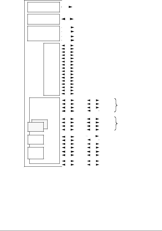
The DSP56824 provides two identical SPIs—SPI0 and SPI1. Figure 7-1 on page 7-2 shows SPI0 and SPI1.
Serial Peripheral Interface |
7-1 |
Serial Peripheral Interface
External
Address MUX
External
Data Switch
Bus Control
General-
Purpose
I/O
Peripheral
Communications
Interfaces
SPI (x2)
SSI
Timers
|
|
|
|
|
|
Default |
|
|
Alternate |
|
|
|||||||||||
|
|
|
|
|
|
Function |
|
|
Function |
|
|
|||||||||||
|
|
|
|
|
|
A15–A0 |
|
|
|
|
|
|||||||||||
|
|
|
|
|
|
|
|
|
|
|
||||||||||||
|
|
|
|
|
|
D15–D0 |
|
|
|
|
|
|||||||||||
|
|
|
|
|
|
|
|
|
|
|||||||||||||
|
|
|
|
|
|
|
|
|
|
|
|
|
|
|
|
|
|
|
|
|
||
|
|
|
|
|
|
RD |
|
|
|
|
|
|
|
|
|
|
|
|
|
|
||
|
|
|
|
|
|
|
|
|
|
|
|
|
|
|
|
|
|
|
|
|
||
|
|
|
|
|
|
|
|
|
|
|
|
|
|
|
|
|
|
|
|
|||
|
|
|
|
|
|
WR |
|
|
|
|
|
|
|
|
|
|
|
|
|
|||
|
|
|
|
|
|
|
|
|
|
|
|
|
|
|
|
|
|
|
|
|||
|
|
|
|
|
|
|
|
|
|
|
|
|
|
|
|
|||||||
|
|
|
|
|
|
PS |
|
|
|
|
|
|
|
|
|
|
||||||
|
|
|
|
|
|
|
|
|
|
|
|
|
|
|
|
|
|
|
|
|
|
|
|
|
|
|
|
|
DS |
|
|
|
|
|
|||||||||||
|
|
|
|
|
|
|
|
|
|
|||||||||||||
|
|
|
|
|
|
PB0 |
|
|
|
|
|
|||||||||||
|
|
|
|
|
|
|
|
|
|
|
||||||||||||
|
|
|
|
|
|
PB1 |
|
|
|
|
|
|||||||||||
|
|
|
|
|
|
|
|
|
|
|
||||||||||||
|
|
|
|
|
|
PB2 |
|
|
|
|
|
|||||||||||
|
|
|
|
|
|
|
|
|
|
|
||||||||||||
|
|
|
|
|
|
PB3 |
|
|
|
|
|
|||||||||||
|
|
|
|
|
|
|
|
|
|
|
||||||||||||
|
|
|
|
|
|
PB4 |
|
|
|
|
|
|||||||||||
|
|
|
|
|
|
|
|
|
|
|
||||||||||||
|
|
|
|
|
|
PB5 |
|
|
|
|
|
|||||||||||
|
|
|
|
|
|
|
|
|
|
|
||||||||||||
|
|
|
|
|
|
PB6 |
|
|
|
|
|
|||||||||||
|
|
|
|
|
|
|
|
|
|
|
||||||||||||
|
|
|
|
|
|
PB7 |
|
|
|
|
|
|||||||||||
|
|
|
|
|
|
|
|
|
|
|
||||||||||||
|
|
|
|
|
|
PB8 |
|
|
|
|
|
|||||||||||
|
|
|
|
|
|
|
|
|
|
|
||||||||||||
|
|
|
|
|
|
PB9 |
|
|
|
|
|
|||||||||||
|
|
|
|
|
|
|
|
|
|
|
||||||||||||
|
|
|
|
|
|
PB10 |
|
|
|
|
|
|||||||||||
|
|
|
|
|
|
|
|
|
|
|
||||||||||||
|
|
|
|
|
|
PB11 |
|
|
|
|
|
|||||||||||
|
|
|
|
|
|
|
|
|
|
|
||||||||||||
|
|
|
|
|
|
PB12 |
|
|
|
|
|
|||||||||||
|
|
|
|
|
|
|
|
|
|
|
||||||||||||
|
|
|
|
|
|
PB13 |
|
|
|
|
|
|||||||||||
|
|
|
|
|
|
|
|
|
|
|
||||||||||||
|
|
|
|
|
|
PB14 |
|
|
|
|
|
|||||||||||
|
|
|
|
|
|
|
|
|
|
|
||||||||||||
|
|
|
|
|
|
XCOLF |
/PB15 |
|
|
|
|
|
||||||||||
|
|
|
|
|
|
|
|
|
|
|
||||||||||||
|
|
|
|
|
|
|
|
|
|
|
|
|
|
|
|
|
|
|
|
|
|
|
|
|
|
|
|
|
PC0 |
|
|
|
|
|
|
|
MISO0 |
|
|
||||||
|
|
|
|
|
|
|
|
|
|
|
|
|
||||||||||
|
|
|
|
|
|
PC1 |
|
|
|
|
|
|
|
MOSI0 |
SPI0 |
|
||||||
|
|
|
|
|
|
|
|
|
|
|
|
|||||||||||
|
|
|
|
|
|
PC2 |
|
|
|
|
|
|
|
SCK0 |
|
|||||||
|
|
|
|
|
|
|
|
|
|
|
|
|
|
|
||||||||
|
|
|
|
|
|
PC3 |
|
|
|
|
|
SS0 |
|
|
||||||||
|
|
|
|
|
|
|
|
|
|
|
|
|||||||||||
|
|
|
|
|
PC4 |
|
|
|
|
|
|
|
MISO1 |
|
|
|||||||
|
|
|
|
|
|
|
|
|
|
|
||||||||||||
|
|
|
|
|
PC5 |
|
|
|
|
|
|
|
MOSI1 |
SPI1 |
|
|||||||
|
|
|
|
|
|
|
|
|
|
|||||||||||||
|
|
|
|
|
PC6 |
|
|
|
|
|
|
|
|
SCK1 |
|
|||||||
|
|
|
|
|
|
|
|
|
|
|
|
|
|
|||||||||
|
|
|
|
|
PC7 |
|
|
|
|
|
|
|
SS1 |
|
|
|||||||
|
|
|
|
|
|
|
|
|
|
|
||||||||||||
|
|
|
|
|
|
|
|
|
|
|
|
|
|
|
|
|
|
|
|
|
|
|
|
|
|
|
|
|
PC8 |
|
|
|
|
STD |
|
|
|||||||||
|
|
|
|
|
|
|
|
|
|
|
||||||||||||
|
|
|
|
|
|
|
|
|||||||||||||||
|
|
|
|
|
|
PC9 |
|
|
|
|
SRD |
|
|
|||||||||
|
|
|
|
|
|
|
|
|
|
|
|
|||||||||||
|
|
|
|
|
|
|
|
|||||||||||||||
|
|
|
|
|
|
PC10 |
|
|
|
|
|
|
|
STCK |
|
|
||||||
|
|
|
|
|
|
|
|
|
|
|
|
|
||||||||||
|
|
|
|
|
|
PC11 |
|
|
|
|
|
|
|
STFS |
|
|
||||||
|
|
|
|
|
|
|
|
|
|
|
|
|
||||||||||
|
|
|
|
|
|
PC12 |
|
|
|
|
|
|
|
SRCK |
|
|
||||||
|
|
|
|
|
|
|
|
|
|
|
|
|
||||||||||
|
|
|
|
|
|
PC13 |
|
|
|
|
|
|
|
SRFS |
|
|
||||||
|
|
|
|
|
|
|
|
|
|
|
|
|
||||||||||
|
|
|
|
|
|
PC14 |
|
|
|
|
|
|
|
TIO01 |
|
|
||||||
|
|
|
|
|
|
|
|
|
|
|
|
|||||||||||
|
|
|
|
|
|
PC15 |
|
|
|
|
|
|
|
TIO2 |
|
AA0144 |
||||||
|
|
|
|
|
|
|
|
|
|
|
||||||||||||
|
|
|
|
|
|
|
|
|
|
|
|
|
|
|
|
|
|
|
|
|
|
|
Figure 7-1. DSP56824 Input/Output Block Diagram
7-2 |
DSP56824 User’s Manual |
|