

- •List of Figures
- •List of Tables
- •List of Examples
- •About This Book
- •1.1 DSP56824 Architecture Overview
- •1.1.1 DSP56824 Peripheral Blocks
- •1.1.1.1 On-Chip Memory
- •1.1.1.2 External Memory Interface (Port A)
- •1.1.1.3 General-Purpose Input/Output Port (Port B)
- •1.1.1.4 Programmable I/O Port (Port C)
- •1.1.1.5 Serial Peripheral Interface (SPI)
- •1.1.1.6 Synchronous Serial Interface (SSI)
- •1.1.1.7 General-Purpose Timer Module
- •1.1.1.8 On-Chip Clock Synthesis Block
- •1.1.1.9 COP/RTI Module
- •1.1.1.10 JTAG/OnCE™ Port
- •1.1.2 DSP56824 Peripheral Interrupts
- •1.2 DSP56800 Core Description
- •1.2.1 Data Arithmetic Logic Unit (Data ALU)
- •1.2.2 Address Generation Unit (AGU)
- •1.2.3 Program Controller and Hardware Looping Unit
- •1.2.4 Bit-Manipulation Unit
- •1.2.5 Address and Data Buses
- •1.2.6 On-Chip Emulation (OnCE) Module
- •1.3 DSP56800 Programming Model
- •1.4 Code Development on the DSP56824
- •2.1 Power and Ground Signals
- •2.2 Clock and Phase Lock Loop (PLL) Signals
- •2.3 External Memory Interface (Port A)
- •2.4 Interrupt and Mode Control Signals
- •2.5 GPIO Signals
- •2.6 Serial Peripheral Interface (SPI) Signals
- •2.7 Synchronous Serial Interface (SSI) Signals
- •2.8 Timer Module Signals
- •2.9 JTAG/OnCE Port Signals
- •3.1 DSP56824 Memory Map
- •3.1.1 X Data Memory
- •3.1.2 Operating Mode Register (OMR)
- •3.1.2.1 Nested Looping (NL)—Bit 15
- •3.1.2.2 Reserved Bits—Bits 14–9
- •3.1.2.3 Condition Codes (CC)—Bit 8
- •3.1.2.4 Reserved Bit—Bit 7
- •3.1.2.5 Stop Delay (SD)—Bit 6
- •3.1.2.6 Rounding (R)—Bit 5
- •3.1.2.7 Saturation (SA)—Bit 4
- •3.1.2.8 External X Memory (EX)—Bit 3
- •3.1.2.9 Reserved Bit—Bit 2
- •3.1.3 DSP56824 Status Register (SR)
- •3.1.4 On-Chip Peripheral Memory Map
- •3.1.5 Program Memory Map
- •3.2 DSP56824 Operating Modes
- •3.2.1 Single Chip Bootstrap Mode (Mode 0)
- •3.2.2 Single Chip User (Mode 1)
- •3.2.3 Normal Expanded Mode (Mode 2)
- •3.2.4 Development Mode (Mode 3)
- •3.3 DSP56824 Reset and Interrupt Vectors
- •3.3.1 DSP56824 Interrupt Priority Register (IPR)
- •3.3.2 Interrupt Priority Structure
- •4.1 External Memory Port Architecture
- •4.2 Port A Description
- •4.2.1 Bus Control Register (BCR)
- •4.2.1.1 Reserved Bits—Bits 15–10
- •4.2.1.2 Drive (DRV)—Bit 9
- •4.2.1.3 Reserved Bit—Bit 8
- •4.2.2 Pins in Different Processing States
- •5.1 Port B Programming Model
- •5.1.1 Port B Data Direction Register (PBDDR)
- •5.1.2 Port B Data (PBD) Register
- •5.1.2.1 PBD Bit Values for General-Purpose Inputs
- •5.1.2.2 PBD Bit Values for General-Purpose Outputs
- •5.1.2.3 PBD Bit Values for Interrupt Inputs
- •5.1.3 Port B Interrupt (PBINT) Register
- •5.2 Port B Interrupt Generation
- •5.3 Port B Programming Examples
- •5.3.1 Receiving Data on Port B
- •5.3.2 Sending Data on Port B
- •5.3.3 Looping Data on Port B
- •5.3.4 Generating Interrupts on Port B
- •6.1 Port C Programming Model
- •6.1.1 Port C Control (PCC) Register
- •6.1.2 Port C Data Direction Register (PCDDR)
- •6.1.3 Port C Data (PCD) Register
- •6.2 Port C Programming Examples
- •6.2.1 Receiving Data on Port C GPIO Pins
- •6.2.2 Sending Data on Port C GPIO Pins
- •6.2.3 Looping Data on Port C GPIO Pins
- •7.1 SPI Architecture
- •7.2 SPI Programming Model
- •7.2.1 SPI Control Registers (SPCR0 and SPCR1)
- •7.2.1.1 Reserved Bits—Bits 15–9
- •7.2.1.2 SPI Clock Rate Select (SPR[2:0])—Bits 8, 1–0
- •7.2.1.3 SPI Interrupt Enable (SPIE)—Bit 7
- •7.2.1.4 SPI Enable (SPE)—Bit 6
- •7.2.1.5 Wired-OR Mode (WOM)—Bit 5
- •7.2.1.6 Master Mode Select (MST)—Bit 4
- •7.2.1.7 Clock Polarity (CPL)—Bit 3
- •7.2.1.8 Clock Phase (CPH)—Bit 2
- •7.2.2 SPI Status Register (SPSR0 and SPSR1)
- •7.2.2.1 Reserved Bits—Bits 15–8
- •7.2.2.2 SPI Interrupt Complete Flag (SPIF)—Bit 7
- •7.2.2.3 Write Collision (WCOL)—Bit 6
- •7.2.2.4 Reserved Bit—Bit 5
- •7.2.2.5 Mode Fault (MDF)—Bit 4
- •7.2.2.6 Reserved Bits—Bits 3–0
- •7.2.3 SPI Data Registers (SPDR0 and SPDR1)
- •7.3 SPI Data and Control Pins
- •7.4 SPI System Errors
- •7.4.1 SPI Mode-Fault Error
- •7.4.2 SPI Write-Collision Error
- •7.4.3 SPI Overrun
- •7.5 Configuring Port C for SPI Functionality
- •7.6 Programming Examples
- •7.6.1 Configuring an SPI Port as Master
- •7.6.2 Configuring an SPI Port as Slave
- •7.6.3 Sending Data from Master to Slave
- •8.1 SSI Architecture
- •8.1.1 SSI Clocking
- •8.1.2 SSI Clock and Frame Sync Generation
- •8.2 SSI Programming Model
- •8.2.1 SSI Transmit Shift Register (TXSR)
- •8.2.2 SSI Transmit Data Buffer Register
- •8.2.3 SSI Transmit Data (STX) Register
- •8.2.4 SSI Receive Shift Register (RXSR)
- •8.2.5 SSI Receive Data Buffer Register
- •8.2.6 SSI Receive Data (SRX) Register
- •8.2.7 SSI Transmit and Receive Control Registers
- •8.2.7.1 Prescaler Range (PSR)—Bit 15
- •8.2.7.2 Word Length Control (WL[1:0])—Bits 14–13
- •8.2.7.3 Frame Rate Divider Control (DC[4:0])—Bits 12–8
- •8.2.7.4 Prescale Modulus Select (PM[7:0])—Bits 7–0
- •8.2.8 SSI Control Register 2 (SCR2)
- •8.2.8.1 Receive Interrupt Enable (RIE)—Bit 15
- •8.2.8.2 Transmit Interrupt Enable (TIE)—Bit 14
- •8.2.8.3 Receive Enable (RE)—Bit 13
- •8.2.8.4 Transmit Enable (TE)—Bit 12
- •8.2.8.5 Receive Buffer Enable (RBF)—Bit 11
- •8.2.8.6 Transmit Buffer Enable (TBF)—Bit 10
- •8.2.8.7 Receive Direction (RXD)—Bit 9
- •8.2.8.8 Transmit Direction (TXD)—Bit 8
- •8.2.8.9 Synchronous Mode (SYN)—Bit 7
- •8.2.8.10 Transmit Shift Direction (TSHFD)—Bit 6
- •8.2.8.11 Transmit Clock Polarity (TSCKP)—Bit 5
- •8.2.8.12 SSI Enable (SSIEN)—Bit 4
- •8.2.8.13 Network Mode (NET)—Bit 3
- •8.2.8.14 Frame Sync Invert (FSI)—Bit 2
- •8.2.8.15 Frame Sync Length (FSL)—Bit 1
- •8.2.8.16 Early Frame Sync (EFS)—Bit 0
- •8.2.9 SSI Control/Status Register (SCSR)
- •8.2.9.1 Reserved Bit—Bit 15
- •8.2.9.2 Receive Shift Direction (RSHFD)—Bit 14
- •8.2.9.3 Receive Clock Polarity (RSCKP)—Bit 13
- •8.2.9.4 Reserved Bits—Bits 12–11
- •8.2.9.5 Receive Frame Sync Invert (RFSI)—Bit 10
- •8.2.9.6 Receive Frame Sync Length (RFSL)—Bit 9
- •8.2.9.7 Receive Early Frame Sync (REFS)—Bit 8
- •8.2.9.8 Receive Data Register Full (RDF)—Bit 7
- •8.2.9.9 Transmit Data Register Empty (TDE)—Bit 6
- •8.2.9.10 Receiver Overrun Error (ROE)—Bit 5
- •8.2.9.11 Transmitter Underrun Error (TUE)—Bit 4
- •8.2.9.12 Transmit Frame Sync (TFS)—Bit 3
- •8.2.9.13 Receive Frame Sync (RFS)—Bit 2
- •8.2.9.14 Receive Data Buffer Full (RDBF)—Bit 1
- •8.2.9.15 Transmit Data Buffer Empty (TDBE)—Bit 0
- •8.2.10 SSI Time Slot Register (STSR)
- •8.3 SSI Data and Control Pins
- •8.4 SSI Operating Modes
- •8.4.1 Normal Mode
- •8.4.1.1 Normal Mode Transmit
- •8.4.1.2 Normal Mode Receive
- •8.4.2 Network Mode
- •8.4.2.1 Network Mode Transmit
- •8.4.2.2 Network Mode Receive
- •8.4.3 Gated Clock Operation
- •8.5 SSI Reset and Initialization Procedure
- •8.6 Configuring Port C for SSI Functionality
- •9.1 Timer Programming Model
- •9.1.1 Timer Control Registers (TCR01 and TCR2)
- •9.1.1.1 Timer Enable (TE)—Bit 15, Bit 7
- •9.1.1.2 Invert (INV)—Bit 6
- •9.1.1.3 Overflow Interrupt Enable (OIE)—Bit 12, Bit 4
- •9.1.1.4 Timer Output Enable (TO[1:0])—Bits 11–10, Bits 3–2
- •9.1.1.5 Event Select (ES[1:0])—Bits 9–8, Bits 1–0
- •9.1.1.6 Reserved TCR Bits
- •9.1.2 Timer Preload Register (TPR)
- •9.1.3 Timer Count Register (TCT)
- •9.2 Timer Resolution
- •9.3 Timer Interrupt Priorities
- •9.4 Event Counting with the Timer Module
- •9.5 Timer Module Low-Power Operation
- •9.5.1 Turning Off the Entire Timer Module
- •9.5.2 Turning Off Any Timer Not in Use
- •9.5.3 Lowering the Timer Frequency
- •9.5.4 Running the Timer in Wait Mode
- •9.5.5 Running the Timer in Stop Mode
- •9.6 Timer Module Timing Diagrams
- •9.7 Configuring Port C for Timer Functionality
- •10.1 Timing System Architecture
- •10.1.1 Oscillator
- •10.1.2 Phase Lock Loop (PLL)
- •10.1.3 Prescaler
- •10.1.4 Clockout Multiplexer (MUX)
- •10.1.5 Control Registers
- •10.2 Clock Synthesis Programming Model
- •10.2.1 PLL Control Register 1 (PCR1)
- •10.2.1.1 Reserved Bit—Bit 15
- •10.2.1.2 PLL Enable (PLLE)—Bit 14
- •10.2.1.3 PLL Power Down (PLLD)—Bit 13
- •10.2.1.4 Low Power Stop (LPST)—Bit 12
- •10.2.1.5 Test Enable (TSTEN)—Bit 11
- •10.2.1.6 Prescaler Divider (PS[2:0])—Bits 10–8
- •10.2.1.7 CLKO Select (CS[1:0])—Bits 7–6
- •10.2.1.8 Reserved Bits—Bits 5–4
- •10.2.1.9 VCO Curve Select (VCS0)—Bit 3
- •10.2.1.10 Reserved Bits—Bits 2–0
- •10.2.2 PLL Control Register 0 (PCR0)
- •10.2.2.1 Reserved Bit—Bit 15
- •10.2.2.2 Feedback Divider (YD[9:0])—Bits 14–5
- •10.2.2.3 Reserved Bits—Bits 4–0
- •10.3 Low-Power Wait and Stop Modes
- •10.3.2 COP, Realtime Clock and CLKO Pin Enabled
- •10.3.3 PLL and CLKO Pin Enabled
- •10.3.4 CLKO Pin Enabled
- •10.3.5 Everything Disabled
- •10.4 PLL Lock
- •10.4.1 PLL Programming Example
- •10.4.2 Changing the PLL Frequency
- •10.4.3 Turning Off the PLL Before Entering Stop Mode
- •10.5 PLL Module Low-Power Operation
- •10.5.1 Turning Off the Entire Clock Synthesis Module
- •10.5.2 Turning Off the Prescaler Divider When Not in Use
- •10.5.3 Turning Off the PLL When Not in Use
- •10.5.4 Turning Off the CLKO Pin When Not in Use
- •11.1 COP and Real-Time Timer Architecture
- •11.2 COP and RTI Timer Programming Model
- •11.2.1 COP and RTI Control Register (COPCTL)
- •11.2.1.1 COP Enable (CPE)—Bit 15
- •11.2.1.2 COP Timer Divider (CT)—Bit 14
- •11.2.1.3 Reserved Bits—Bits 13–12
- •11.2.1.4 RTI Timer Enable (RTE)—Bit 11
- •11.2.1.5 RTI Enable (RTIE)—Bit 10
- •11.2.1.6 RTI Flag (RTIF)—Bit 9
- •11.2.1.7 RTI Prescaler (RP)—Bit 8
- •11.2.1.8 RTI/COP Divider (DV[7:0])—Bits 7–0
- •11.2.2 COP and RTI Count (COPCNT) Register
- •11.2.2.1 Reserved Bits—Bits 15–13
- •11.2.2.2 RTI/COP Divider (DV[7:0])—Bits 12–5
- •11.2.2.3 RTI Prescaler (RP[1:0])—Bits 4–3
- •11.2.2.4 Scaler (SC[2:0])—Bits 2–0
- •11.2.3 COP Reset (COPRST) Register
- •11.3 Programming the COP and RTI Timers
- •11.3.1 COP and RTI Timer Resolution
- •11.3.2 COP/RTI Timer Low-Power Operation
- •11.3.3 Programming Example
- •12.1 Combined JTAG/OnCE Interface Overview
- •12.2 JTAG/OnCE Port Pinout
- •12.3 OnCE Module Architecture
- •12.3.1 OnCE Port Block Diagram
- •12.3.2 OnCE Programming Model
- •12.3.3 OnCE State Machine and Control Block
- •12.4 Command, Status, and Control Registers
- •12.4.1 OnCE Shift Register (OSHR)
- •12.4.2 OnCE Command Register (OCMDR)
- •12.4.3 OnCE Decoder (ODEC)
- •12.4.4 OnCE Control Register (OCR)
- •12.4.4.1 COP Timer Disable (COPDIS)—Bit 15
- •12.4.4.2 DE Pin Output Enable (DE)—Bit 14
- •12.4.4.3 Breakpoint Configuration (BK[4:0])—Bits 13–9
- •12.4.4.4 Debug Request Mask (DRM)—Bit 8
- •12.4.4.5 FIFO Halt (FH)—Bit 7
- •12.4.4.6 Event Modifier (EM[1:0])—Bits 6–5
- •12.4.4.7 Power Down Mode (PWD)—Bit 4
- •12.4.4.8 Breakpoint Selection (BS[1:0])—Bits 3–2
- •12.4.4.9 Breakpoint Enable (BE[1:0])—Bits 1–0
- •12.4.5 OnCE Breakpoint 2 Control Register (OBCTL2)
- •12.4.5.1 Reserved OBCTL2 Register Bits
- •12.4.5.2 Enable (EN)—Bit 2
- •12.4.5.3 Invert (INV)—Bit 1
- •12.4.5.4 Data/Address Select (DAT)—Bit 0
- •12.4.6 OnCE Status Register (OSR)
- •12.4.6.1 Reserved OSR Bits—Bits 7–5
- •12.4.6.2 OnCE Core Status (OS[1:0])—Bits 4–3
- •12.4.6.3 Trace Occurrence (TO)—Bit 2
- •12.4.6.4 Hardware Breakpoint Occurrence (HBO)—Bit 1
- •12.4.6.5 Software Breakpoint Occurrence (SBO)—Bit 0
- •12.5 Breakpoint and Trace Registers
- •12.5.1 OnCE Breakpoint/Trace Counter Register (OCNTR)
- •12.5.2 OnCE Memory Address Latch (OMAL) Register
- •12.5.3 OnCE Breakpoint Address Register (OBAR)
- •12.5.4 OnCE Memory Address Comparator (OMAC)
- •12.5.5 OnCE Breakpoint and Trace Section
- •12.6 Pipeline Registers
- •12.6.1 OnCE PAB Fetch Register (OPABFR)
- •12.6.2 OnCE PAB Decode Register (OPABDR)
- •12.6.3 OnCE PAB Execute Register (OPABER)
- •12.6.4 OnCE PAB Change-of-Flow FIFO (OPFIFO)
- •12.6.5 OnCE PDB Register (OPDBR)
- •12.6.6 OnCE PGDB Register (OPGDBR)
- •12.6.7 OnCE FIFO History Buffer
- •12.7 Breakpoint 2 Architecture
- •12.8 Breakpoint Configuration
- •12.8.1 Programming the Breakpoints
- •12.8.2 OnCE Trace Logic Operation
- •12.9 The Debug Processing State
- •12.9.1 OnCE Normal, Debug, and Stop Modes
- •12.9.2 Entering Debug Mode
- •12.9.2.1 JTAG DEBUG_REQUEST and the Debug Event Pin
- •12.9.2.2 Software Request During Normal Activity
- •12.9.2.3 Trigger Events (Breakpoints and Trace Modes)
- •12.9.2.5 Exiting Debug Mode
- •12.10 Accessing the OnCE Module
- •12.10.1 Primitive JTAG Sequences
- •12.10.2 Entering the JTAG Test-Logic-Reset State
- •12.10.3 Loading the JTAG Instruction Register
- •12.10.4 Accessing a JTAG Data Register
- •12.10.4.1 JTAG/OnCE Interaction: Basic Sequences
- •12.10.4.2 Executing a OnCE Command by Reading the OCR
- •12.10.4.3 Executing a OnCE Command by Writing the OCNTR
- •12.10.4.4 OSR Status Polling
- •12.10.4.5 JTAG IR Status Polling
- •12.10.4.6 TRST/DE Pin Polling
- •12.10.5 Serial Protocol Description
- •12.10.5.1 Entering Debug Mode from User Mode
- •12.10.5.2 Entering Debug Mode from DSP Reset
- •12.10.5.3 Polling for OnCE Status
- •12.10.5.4 Setting Breakpoints in User Mode
- •12.10.5.5 Reading Pipeline Information in User Mode
- •12.10.5.6 Displaying a Specified Register
- •12.10.5.7 Displaying X Memory Area Starting at Address xxxx
- •12.10.5.8 Returning from Debug Mode to Normal Mode
- •12.10.5.9 Recovering from STOP or WAIT Execution
- •12.11 Using the OnCE Port
- •12.11.1 Beginning Debug Activity
- •12.11.2 Displaying a Specified Register
- •12.11.3 Displaying X Memory Area Starting at Address xxxx
- •12.11.4 Returning from Debug Mode to Normal Mode
- •12.12 OnCE Unit Low-Power Operation
- •13.1 JTAG/OnCE Port Pinout
- •13.2 JTAG Port Architecture
- •13.2.1 JTAG Instruction Register (IR) and Decoder
- •13.2.2 JTAG Chip Identification (CID) Register
- •13.2.3 JTAG Boundary Scan Register (BSR)
- •13.2.4 JTAG Bypass Register
- •13.3 TAP Controller
- •13.4 DSP56824 Restrictions
- •A.1 Design Considerations
- •A.1.1 Boot Source Selection
- •A.1.1.1 Bootstrapping from SPI0
- •A.1.1.2 Bootstrapping from Port A
- •A.1.2 COP Reset
- •A.1.3 No Load Option
- •A.2 Bootstrap Listing
- •B.1 DSP56824 BSDL Listing—100-Pin TQFP
- •C.1 Instruction Set Summary
- •C.2 Interrupt, Vector, and Address Tables
- •C.3 Programmer’s Sheets
- •Index
DSP56824 Overview
1.1 DSP56824 Architecture Overview
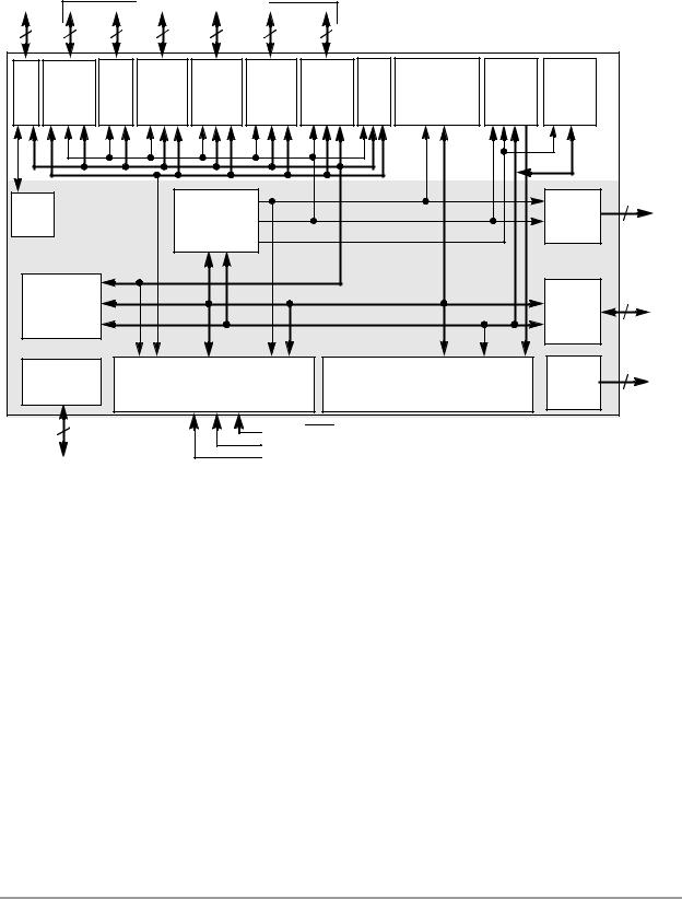
The DSP56824 consists of the DSP56800 core, program and data memory, and peripherals useful for embedded control applications. Figure 1-1 on page 1-2 shows a block diagram of the DSP56824 chip.
16 to 32 GPIO lines
4 |
8 |
8 |
4 |
4 |
6 |
2 |
|
|
|
|
|
|
Program- |
|
Serial |
Serial |
Synch. |
Timer/ |
COP/ |
Program |
Data |
Data |
|
||
|
mable |
|
Periph. |
Periph. |
Serial |
Event |
Memory |
Memory |
Memory |
|
||
PLL Interrupt |
GPIO |
Interface |
Interface |
Interface |
Counters |
RTI |
32K × |
16 ROM |
3584 × |
2048 × |
|
|
|
GPIO |
|
(SPI0) |
(SPI1) |
(SSI) or |
or GPIO |
|
128 × |
16 RAM |
16 RAM |
16 ROM |
|
|
|
|
or GPIO |
or GPIO |
GPIO |
|
|
|
|
|
|
|
|
|
|
|
|
|
|
PAB |
|
|
|
External |
Address |
Clock |
16-Bit |
|
Address |
|
|
|
|
|
|
|||
|
|
|
XAB1 |
|
|
|
Address |
|
||||
Gen. |
DSP56800 |
|
Generation |
|
|
|
|
|
Bus |
|
||
|
|
|
XAB2 |
|
|
|
16 |
|||||
|
Core |
|
Unit |
|
|
|
|
|
Switch |
|||
|
|
|
|
|
|
|
|
|
|
|
||
|
|
|
PGDB |
|
|
|
|
|
XDB2 |
|
||
|
|
|
|
|
|
|
|
|
|
|
||
|
Bit- |
|
PDB |
|
|
|
|
|
|
External |
Data |
|
Manipulation |
|
CGDB |
|
|
|
|
|
|
Data |
|
||
|
Unit |
|
|
|
|
|
|
|
Bus |
16 |
||
|
|
|
|
|
|
|
|
|
|
Switch |
||
|
|
|
|
|
|
|
|
|
|
|
||
JTAG/ |
|
|
|
|
|
|
Data ALU |
|
|
Control |
||
|
|
|
|
|
16 × 16 + 36 → |
36-bit MAC |
Bus |
|
||||
OnCE™ |
|
Program Controller |
|
|
||||||||
|
|
Three 16-bit Input Registers |
Control |
|
||||||||
|
Port |
|
|
|
|
|
4 |
|||||
|
|
|
|
|
|
Two 36-bit Accumulators |
|
|||||
|
|
|
|
|
|
|
|
|||||
|
|
|
|
|
|
|
|
|
||||
|
5 |
|
|
|
MODA/IRQA |
|
|
|
|
|
|
|
|
|
|
|
MODB/IRQB |
|
|
|
|
|
|
||
|
|
|
|
|
|
|
|
|
|
AA1428 |
||
|
|
|
|
|
RESET |
|
|
|
|
|
||
Figure 1-1. DSP56824 Functional Block Diagram
Features of the DSP56824 include the following:
•35 million instructions per second (MIPS) with 70 MHz clock
•On-chip memory
•Off-chip memory expansion capability
—Off-chip expansion to 64K × 16 data memory
—Off-chip expansion to 64K × 16 program memory
•On-chip peripherals (listed in the following subsection)
•2.7 V to 3.6 V power supply
•Very low-power complementary metal-oxide semiconductor (CMOS) design
•Power management circuitry with power-saving wait and multiple stop modes
•Fully static logic with operating frequencies down to DC
1-2 |
DSP56824 User’s Manual |
|