


Port B Programming Examples
5.3.4 Generating Interrupts on Port B
Example 5-4 shows how to configure and use Port B for generating interrupts.
Example 5-4. Generating Interrupts on Port B
;********************* |
|
|
|
;* INTERRUPT example* |
|
|
|
;* for Port B |
* |
|
|
;* of DSP56824 chip * |
|
|
|
;********************* |
|
|
|
START |
EQU |
$0040 |
; Start of program |
BCR |
EQU |
$FFF9 |
; Bus Control Register |
IPR |
EQU |
$FFFB |
; Interrupt Priority Register |
PBD |
EQU |
$FFEC |
; Port B Data |
PBDDR |
EQU |
$FFEB |
; Port B Data Direction Register |
PBINT |
EQU |
$FFEA |
; Port B Interrupt Register |
data_o |
EQU |
$0000 |
; data output |
data_i |
EQU |
$0001 |
; data input |
;************** |
|
|
|
;* Vector setup* |
|
|
|
;************** |
|
|
|
ORG |
P:$0000 |
|
; Cold Boot |
JMP |
START |
|
; also Hardware RESET vector (Mode 0, 1, 3) |
ORG |
P:$E000 |
|
; Warm Boot |
JMP |
START |
|
; Hardware RESET vector (Mode 2) |
ORG |
P:$0014 |
|
; |
JSR |
GPIOISR |
|
; GPIO Interrupt vector |
ORG |
P:START |
|
; Start of program |
;************** |
|
|
|
;* General setup* |
|
|
|
;************** |
|
|
|
MOVEP |
#$0000,X:BCR |
; External Program memory has 0 wait states. |
|
|
|
|
; External data memory has 0 wait states. |
|
|
|
; Port A pins are tri-stated when no |
|
|
|
; external access occurs. |
BFCLR |
#$0200,SR |
; Allow IPL (Interrupt Priority Level) 0. |
|
|
|
|
; -- Enable maskable interrupts. |
;* Port B setup* |
|
|
; -- (peripherals, and so on);************** |
|
|
|
|
;************** |
|
|
|
MOVEP |
#$8000,X:PBINT |
; Enable GPIO interrupt requests for |
|
|
|
|
; rising transitions on PB7. |
MOVEP |
#$FF00,X:PBDDR |
; Select PB0-PB7 as input, PB8-PB15 as output |
|
BFSET |
#$8000,X:IPR |
; Enable GPIO interrupts. |
|
;************** |
|
|
|
;* Main routine* |
|
|
|
;************** |
|
|
; ... |
|
|
|
|
MOVE |
#$0000,X:data_o |
; Initialize “data_o” |
|
TESTPAT |
|
|
; Test Pattern Loop |
MOVE |
X:data_o,X0 |
; Put bits 8-15 of “data_o” on pins PB8-PB15. |
|
MOVEP |
X0,X:PBD |
; Bits going to input pins are ignored. |
|
ADD |
#$0100,X0 |
; Change output pattern: increment by 1. |
|
MOVE |
X0,X:data_o |
; Increment upper byte by 1. |
|
MOVEP |
X:PBD,X0 |
; Read PB0-PB7 into bits 0-7 of “data_i”. |
|
MOVE |
X0,X:data_i |
; Bits 8-15 get values of PB8-PB15 as well. |
|
BRA |
TESTPAT |
|
; ... |
|
|
||
GPIOISR |
|
|
; GPIO Interrupt Service Routine |
RTI |
|
|
; interrupt code |
|
|
|
|
|
|
|
|
Port B GPIO Functionality |
5-11 |

Port B GPIO Functionality
5-12 |
DSP56824 User’s Manual |
|
Chapter 6
Port C GPIO Functionality
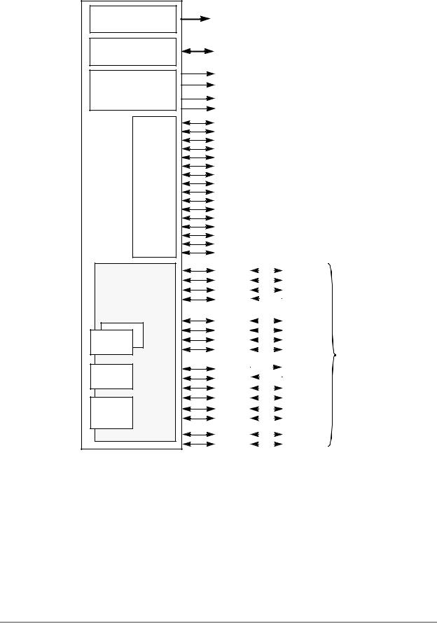
The peripheral communications port (Port C) provides 16 multiplexed programmable I/O pins. These pins may be used as general-purpose input/output (GPIO) pins or allocated to on-chip peripherals—a timer module, two serial peripheral interfaces (SPIs), and a synchronous serial interface (SSI). (See Figure 6-1 on page 6-2.) Each pin is individually programmable.
This section describes how to program the pins for Port C and provides general information about their use as GPIO pins. Specifics for programming the various peripherals represented on Port C are provided in the appropriate sections, as follows:
•SPI module programming specifics are located in Chapter 7, “Serial Peripheral Interface.”
•SSI module programming specifics are located in Chapter 8, “Synchronous Serial Interface.”
•Timer module programming specifics are located in Chapter 9, “Timers.”
The Port C I/O interfaces are intended to minimize system chip count and “glue” logic in many DSP applications. Each I/O interface has its own control, status, and data registers that are treated as memory-mapped peripheral registers by the DSP56824. Each interface has several dedicated interrupt vector addresses and control bits to enable or disable interrupts. This minimizes the overhead associated with servicing the device, since each interrupt source may have its own service routine.
Port C GPIO Functionality |
6-1 |
Port C GPIO Functionality
External
Address MUX
External
Data Switch
Bus Control
General-
Purpose
I/O
Peripheral
Communications
Interfaces
SPI (x2)
SSI
Timers
Default |
|
|
Alternate |
|
|||||||||||
Function |
|
|
Function |
|
|||||||||||
A15–A0 |
|
|
|
|
|||||||||||
D15–D0 |
|
|
|
|
|||||||||||
|
|
|
|
|
|
|
|
|
|
|
|
|
|
||
RD |
|
|
|
|
|
|
|
|
|
|
|
|
|
||
|
|
|
|
|
|
|
|
|
|
|
|
|
|||
WR |
|
|
|
|
|
|
|
|
|
|
|
|
|||
|
|
|
|
|
|
|
|
|
|||||||
PS |
|
|
|
|
|
|
|
|
|
||||||
DS |
|
|
|
|
|||||||||||
PB0 |
|
|
|
|
|||||||||||
PB1 |
|
|
|
|
|||||||||||
PB2 |
|
|
|
|
|||||||||||
PB3 |
|
|
|
|
|||||||||||
PB4 |
|
|
|
|
|||||||||||
PB5 |
|
|
|
|
|||||||||||
PB6 |
|
|
|
|
|||||||||||
PB7 |
|
|
|
|
|||||||||||
PB8 |
|
|
|
|
|||||||||||
PB9 |
|
|
|
|
|||||||||||
PB10 |
|
|
|
|
|||||||||||
PB11 |
|
|
|
|
|||||||||||
PB12 |
|
|
|
|
|||||||||||
PB13 |
|
|
|
|
|||||||||||
PB14 |
|
|
|
|
|||||||||||
XCOLF |
/PB15 |
|
|
|
|
||||||||||
PC0 |
|
|
|
|
|
|
|
MISO0 |
|
||||||
|
|
|
|
|
|
||||||||||
PC1 |
|
|
|
|
|
|
|
MOSI0 |
|
||||||
|
|
|
|
|
|
||||||||||
PC2 |
|
|
|
|
|
|
|
SCK0 |
|
||||||
|
|
|
|
|
|
||||||||||
PC3 |
|
|
|
|
|
SS0 |
|
||||||||
|
|
|
|
|
|||||||||||
PC4 |
|
|
|
|
|
|
|
MISO1 |
|
||||||
|
|
|
|
|
|||||||||||
PC5 |
|
|
|
|
|
|
|
MOSI1 |
|
||||||
|
|
|
|
|
|||||||||||
PC6 |
|
|
|
|
|
|
|
SCK1 |
|
||||||
|
|
|
|
|
|||||||||||
PC7 |
|
|
|
|
|
|
|
SS1 |
Port C |
||||||
|
|
|
|
||||||||||||
|
|
|
|
|
|
|
|
|
|
|
|
|
|
|
|
PC8 |
|
|
|
|
STD |
|
|||||||||
|
|
|
|
||||||||||||
PC9 |
|
|
|
|
SRD |
|
|||||||||
|
|
|
|
|
|||||||||||
PC10 |
|
|
|
|
|
|
|
STCK |
|
||||||
|
|
|
|
|
|
||||||||||
PC11 |
|
|
|
|
|
|
|
STFS |
|
||||||
|
|
|
|
|
|
||||||||||
PC12 |
|
|
|
|
|
|
|
SRCK |
|
||||||
|
|
|
|
|
|
||||||||||
PC13 |
|
|
|
|
|
|
|
SRFS |
|
||||||
|
|
|
|
|
|
||||||||||
PC14 |
|
|
|
|
|
|
|
TIO01 |
|
||||||
|
|
|
|
|
|
||||||||||
PC15 |
|
|
|
|
|
|
|
TIO2 |
AA0137 |
||||||
|
|
|
|
|
|||||||||||
|
|
|
|
|
|
|
|
|
|
|
|
|
|
|
|
Figure 6-1. DSP56824 Input/Output Block Diagram
6-2 |
DSP56824 User’s Manual |
|