


External Memory Interface
4.2.2 Pins in Different Processing States
The DSP56800 core can be in one of six processing states (also called modes):
•Normal
•Exception
•Reset
•Wait
•Stop
•Debug
In the normal mode, each instruction cycle has two possible cases—either the processor needs to perform an external access, or all accesses are done internally. Exception processing is similar. For the case of an external access, the address and bus control pins are driven to perform a normal bus cycle, and the data bus is also driven if the access is a write cycle.
For the case where there is no external access on a particular instruction cycle, one of two things may occur. The external address bus and control pins can remain driven with their previous values, or they can be tri-stated.
The Reset mode always tri-states the external address bus and internally pulls control pins high. The stop and wait modes, however, either tri-state the address bus and control pins or let them remain driven with their previous values. This selection is made based on the value of the DRV bit in the BCR. Table 4-2 and Table 4-3 describe the operation of the external memory port in these different modes. The debug mode is a special state used to debug and test programming code. This state is discussed in detail in Chapter 9 of the DSP56800 Family Manual, but is not described in the following tables.
Table 4-2. Port A Operation with DRV Bit = 0
Mode |
|
|
|
|
Pins |
|
|||||
|
|
|
|
|
|
|
|
|
|
|
|
|
A0–A15 |
|
PS, |
|
DS, |
|
RD, |
|
WR |
|
D0–D15 |
|
|
|
|
||||||||
|
|
|
|
||||||||
Normal mode, external access |
Driven |
Driven |
Driven |
||||||||
|
|
|
|
||||||||
Normal mode, internal access |
Tri-stated |
Tri-stated |
Tri-stated |
||||||||
|
|
|
|
||||||||
Stop mode |
Tri-stated |
Tri-stated |
Tri-stated |
||||||||
|
|
|
|
||||||||
Wait mode |
Tri-stated |
Tri-stated |
Tri-stated |
||||||||
|
|
|
|
||||||||
Reset mode |
Tri-stated |
Pulled high internally |
Tri-stated |
||||||||
|
|
|
|
|
|
|
|
|
|
|
|
4-6 |
DSP56824 User’s Manual |
|

|
|
|
|
|
|
|
|
|
|
|
Port A Description |
|
Table 4-3. Port A Operation with DRV Bit = 1 |
|
|
||||||||||
|
|
|
|
|
|
|
|
|||||
Mode |
|
|
|
|
Pins |
|
|
|||||
|
|
|
|
|
|
|
|
|
|
|
|
|
|
A0–A15 |
|
|
|
|
|
|
|
|
|
|
D0–D15 |
|
|
PS, |
DS, |
RD, |
WR |
|||||||
|
|
|
|
|
||||||||
|
|
|
|
|
||||||||
Normal mode, external access |
Driven |
Driven |
|
Driven |
||||||||
|
|
|
|
|
||||||||
Normal mode, internal access |
Driven |
Driven |
|
Tri-stated |
||||||||
|
|
|
|
|
||||||||
Stop mode |
Driven |
Driven |
|
Tri-stated |
||||||||
|
|
|
|
|
||||||||
Wait mode |
Driven |
Driven |
|
Tri-stated |
||||||||
|
|
|
|
|
||||||||
Reset mode |
Tri-stated |
Pulled high internally |
|
Tri-stated |
||||||||
|
|
|
|
|
|
|
|
|
|
|
|
|
The data lines are driven during normal mode, external fetch, only during an external write cycle.
External Memory Interface |
4-7 |

External Memory Interface
4-8 |
DSP56824 User’s Manual |
|

Chapter 5
Port B GPIO Functionality
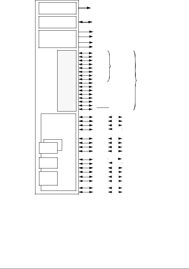
This section describes in detail the pins and programming specifics for Port B of the DSP56824. Port B is a dedicated general-purpose input/output (GPIO) port that provides 16 programmable I/O pins. Port B can be configured to generate an interrupt when a transition is detected on any of its lower eight pins, PB7–PB0, if they are configured as inputs. The upper eight pins, PB15–PB8, do not offer this interrupt functionality. During reset, the XCOLF functionality of PB15 allows selecting a low-frequency clock. For more information on XCOLF, see the DSP56824 Technical Data Sheet. Figure 5-1 on page 5-2 shows a block diagram of the I/O of the DSP56824.
NOTE:
After reset, all Port B pins are inputs.
Port B GPIO Functionality |
5-1 |
Port B GPIO Functionality
External
Address MUX
External
Data Switch
Bus Control
General-
Purpose
I/O
Peripheral
Communications
Interfaces
SPI (x2)
SSI
Timers
Default |
Alternate |
||||
Function |
Function |
||||
A15–A0 |
|
||||
D15–D0 |
|
||||
|
|
|
|
||
RD |
|
|
|
||
|
|
|
|||
WR |
|
|
|||
|
|
||||
PS |
|
|
|||
DS |
|
||||
PB0 |
|
||||
PB1 |
Interrupts |
||||
PB2 |
|||||
available |
|||||
PB3 |
|||||
PB4 |
on these |
||||
PB5 |
pins |
||||
PB6 |
|||||
|
|||||
PB7 |
Port B |
||||
PB8 |
|||||
|
|||||
PB9 |
|
||||
PB10
PB11
PB12
PB13
PB14
XCOLF/PB15
PC0 |
|
|
|
|
MISO0 |
|
||
|
|
|
||||||
PC1 |
|
|
|
|
MOSI0 |
|
||
|
|
|
||||||
PC2 |
|
|
|
|
SCK0 |
|
||
|
|
|
||||||
PC3 |
|
|
|
|
SS0 |
|
||
|
|
|
|
|||||
PC4 |
|
|
|
|
|
MISO1 |
|
|
|
|
|
|
|||||
PC5 |
|
|
|
|
|
MOSI1 |
|
|
|
|
|
|
|||||
PC6 |
|
|
|
|
|
SCK1 |
|
|
|
|
|
|
|||||
PC7 |
|
|
|
|
|
SS1 |
|
|
|
|
|
|
|||||
PC8 |
|
|
|
|
|
STD |
|
|
|
|
|
|
|
|
|||
PC9 |
|
|
|
|
SRD |
|
||
|
|
|
|
|
||||
PC10 |
|
|
|
|
STCK |
|
||
|
|
|
||||||
PC11 |
|
|
|
|
STFS |
|
||
|
|
|
||||||
PC12 |
|
|
|
|
SRCK |
|
||
|
|
|
||||||
PC13 |
|
|
|
|
SRFS |
|
||
|
|
|
||||||
PC14 |
|
|
|
|
TIO01 |
|
||
|
|
|
||||||
PC15 |
|
|
|
|
TIO2 |
AA0134 |
||
|
|
|||||||
|
|
|
|
|
|
|
|
|
Figure 5-1. DSP56824 Input/Output Block Diagram
5-2 |
DSP56824 User’s Manual |
|