

Memory Configuration and Operating Modes
$FFFF |
Program |
64 K |
$FFFF |
X Data |
64 K |
|
|
|
|
||
|
Memory |
|
|
|
|
|
|
|
Memory |
|
|
|
Space |
|
|
|
|
|
|
|
Space |
|
|
|
|
|
|
|
|
$7F |
|
127 |
|
|
|
Interrupt |
|
|
|
||
$0 |
Vectors |
0 |
$0 |
|
0 |
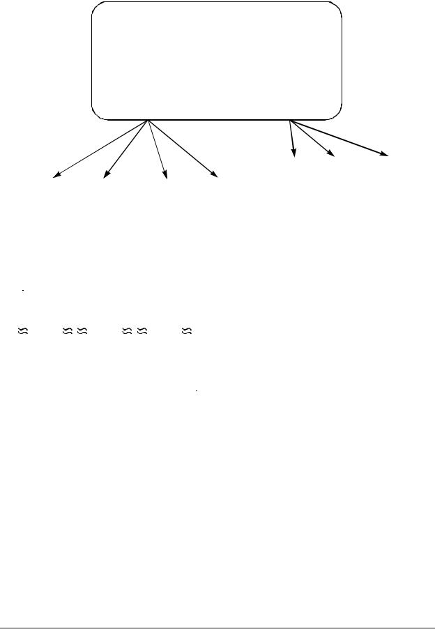
Operating mode and EX bit in OMR determine memory configurations and reset starting address
|
|
|
|
|
|
|
|
|
|
|
|
|
Normal |
EX bit set and |
EX bit set and |
|||||
|
|
|
|
|
|
|
|
|
|
|
|
|
memory map |
using I/O short |
|
all other |
||||
|
|
|
Mode 0 |
|
|
|
Mode 2 |
Mode 3 |
|
(EX = 0) |
|
addressing |
|
addressing |
||||||
|
|
Mode 1 |
|
|
|
|||||||||||||||
$FFFF |
|
|
|
|
|
|
|
|
|
|
$FFFF |
|
|
|
|
|
|
|
|
|
|
|
|
|
|
|
|
|
|
|
On-Chip |
|
|
On-Chip |
|
|
|
|
|||
|
|
|
External |
|
|
|
|
|
|
|
|
$FFC0 |
Peripheral |
|
|
Peripheral |
|
|
|
|
|
|
|
|
External |
|
|
|
|
|
|
|
|
|
|
|
|
|
|||
|
|
|
Program |
|
|
|
|
|
|
|
On-Chip |
|
|
|
|
|
|
|
||
|
|
|
|
Program |
|
Reset Vector |
|
|
|
|
|
|
|
|
|
|
||||
|
|
|
Memory |
|
|
|
|
$FF80 |
Peripheral |
|
|
|
|
|
|
|
||||
|
|
|
|
Memory |
|
External |
|
|
|
|
|
|
|
|
|
|||||
|
|
|
|
|
|
|
|
|
|
|
|
|
|
|
|
|
||||
|
|
|
|
|
|
|
|
Program |
|
|
|
|
|
|
|
|
|
|
|
|
|
|
|
|
|
|
|
|
Memory |
|
|
|
|
|
|
|
|
|
|
|
|
$8000 |
|
|
|
|
|
|
|
|
|
|
External |
|
External |
|
|
|
|
|
|
|
|
Reserved |
|
Reserved |
|
Reserved |
|
|
|
|
|
|
|
External |
|
||||||
|
|
|
|
|
|
|
Data |
|
|
|
|
|
|
|||||||
|
|
|
Internal |
|
Internal |
|
Internal |
|
Program |
|
|
|
|
|
|
|
||||
|
|
|
|
|
|
|
Memory |
|
|
|
|
|
Data |
|
||||||
$7FC0 |
|
Program ROM |
|
Program ROM |
|
Program ROM |
|
Memory |
|
|
|
External |
|
|
|
|||||
|
|
|
|
|
|
|
|
|
|
Memory |
|
|||||||||
|
Internal |
|
Internal |
|
Internal |
|
|
|
|
|
|
Data |
|
|
|
|||||
|
|
|
|
|
|
|
|
|
|
|
|
|
|
|
||||||
|
|
|
|
Bootstrap |
|
|
|
|
|
|
|
Memory |
|
|
|
|
||||
|
|
|
Bootstrap |
|
|
Bootstrap |
|
|
|
|
|
|
|
|
|
|
||||
|
|
|
|
Program ROM |
|
|
|
|
|
|
|
|
|
|
|
|
||||
|
|
|
Program ROM |
|
|
Program ROM |
|
|
|
|
|
|
|
|
|
|
|
|||
|
|
|
|
|
|
|
|
|
|
|
|
|
|
|
|
|
|
|||
$7F80 |
|
Reset Vector |
|
|
|
$2000 |
|
|
|
|
|
|
|
|
||||||
|
|
|
|
|
|
|
|
|
|
|
|
|
|
|
|
|||||
|
Internal |
|
Internal |
|
Internal |
|
|
(Hole) |
|
|
|
|
|
|
|
|||||
|
|
|
|
|
|
|
$1600 |
|
|
|
|
|
|
|
||||||
|
|
|
Program |
|
Program |
|
|
Program |
|
|
|
Internal |
|
|
|
|
|
|
|
|
|
|
|
|
|
|
|
|
|
|
|
|
|
|
|
|
|
||||
|
|
|
ROM |
|
ROM |
|
ROM |
|
|
|
|
|
|
|
|
|
|
|||
|
|
|
|
|
|
|
|
Data RAM |
|
|
|
|
|
|
|
|||||
|
|
|
|
|
|
|
|
|
|
|
|
$1000 |
|
|
|
|
|
|
|
|
$80 |
|
|
|
|
|
|
|
|
|
|
|
|
|
|
|
|
|
|
|
|
|
|
Internal |
|
Internal |
|
Internal |
|
|
|
Internal |
|
|
|
|
|
|
|
|||
|
|
|
|
|
|
|
|
|
|
|
|
|
|
|
||||||
|
|
|
Program |
|
|
|
|
|
Data ROM |
|
|
|
|
|
|
|
||||
|
|
|
|
|
Program |
|
|
|
|
|
|
|
|
|
|
|||||
|
|
|
RAM (write) |
|
Program RAM |
|
|
|
$0800 |
|
|
|
|
|
|
|
|
|||
|
|
|
|
|
RAM (write) |
|
|
Internal |
|
|
|
|
|
|
|
|||||
|
|
|
ROM (read) |
|
(read/write) |
|
|
|
|
|
|
|
|
|
|
|
||||
$0 |
|
|
Reset Vector |
|
|
|
|
ROM (read) |
|
Reset Vector |
$0 |
Data RAM |
|
|
|
|
|
|
|
|
|
|
|
|
|
|
|
|
|
|
|
|
|
|
|
|
|
|
|
AA1432 |
|
Figure 3-1. DSP56824 Memory Map
3.1.1 X Data Memory
The DSP56824 has 3.5K words of on-chip data RAM and 2K words of on-chip data ROM. Also, 128 additional data memory locations are reserved for on-chip peripheral registers (X:$FF80–$FFFF). The internal data memory map contains a non-accessible segment at X:$1600–$1FFF. When the EX bit is cleared, no memory can be accessed in these locations. When the EX bit is set, these locations are accessed as external memory. Any access to these addresses does not access external memory, except when the EX bit is set. These locations should be used by an application only when the EX bit is set exclusively.
For DSP56800 core instructions that perform two reads from the X data memory in a single instruction, the second access using the R3 pointer always occurs to on-chip memory. The internal X data memories decode only the upper 13 bits of XAB2, so the second read is Modulo 8192 to on-chip data memory x:$0, as follows:
3-2 |
DSP56824 User’s Manual |
|

DSP56824 Memory Map
MOVE |
#$A000, R3 |
|
NOP |
|
|
MOVE |
X:(R1)+,Y0 |
X:(R3)+, X0 |
The 2K on-chip X data ROM can only be accessed using the second access (that is, using the R3 pointer) of instructions that perform two parallel reads. On-chip X data ROM is not accessible on the first read or by instructions that perform single reads.
During development, the data that will finally be located in the X data ROM is often located off-chip. Data that will be mapped into on-chip ROM on a factory-programmed production part should be accessed from the external memory in the same manner as in the final target. Because the second read of a dual read instruction can never access off-chip memory, the -o dbl Assembler switch, which breaks a dual read into two equivalent instructions, must be used. This is shown in Example 3-1.
Example 3-1. Breaking a Read Instruction in Two
; Original instruction - X:(R3) accesses the internal ROM
MOVE X:(R0)+N,Y1 X:(R3)-,X0 ;X:(R3) cannot access off-chip memory
;Breaking the instruction into two equivalent
;instructions -- X:(R3) can access off-chip memory
MOVE |
X:(R0)+N,Y1 |
|
MOVE |
X:(R3)-,X0 |
;Now X:(R3) can access off-chip memory |
|
|
|
The X memory can be expanded off-chip for a total of 65,536 addressable locations when the EX bit in the OMR is set. When the EX bit in the OMR is cleared, the X memory contains a total of 62,848
(65,536 – 2,688) addressable memory locations, including both on-chip and off-chip memory. The 2,560 locations of the memory hole and the 128 locations of the dedicated on-chip peripheral registers account for these 2,688 locations.
The external data memory bus access time is controlled by 4 bits of the bus control register (BCR) located at X:$FFF9. This register is shown in Figure 3-2 and described in detail in Chapter 4, “External Memory
Interface.”
BCR— X:$FFF9 |
15 |
14 |
13 |
12 |
11 |
10 |
9 |
8 |
7 |
6 |
5 |
4 |
3 |
2 |
1 |
0 |
|
|
|
|
|
|
|
|
|
|
|
|
|
|
|
|
|
|
|
Bus Control Register |
|
|
|
|
|
|
DRV |
|
|
Wait State Field |
|
|
Wait State Field |
|
|
||
Reset = $00FF |
* |
* |
* |
* |
* |
* |
|
* |
for External X Memory |
for External P Memory |
|
||||||
Read/Write |
|
|
|||||||||||||||
|
|
|
|
|
|
|
|
|
|
|
|
|
|
|
|
|
|
|
|
|
|
|
|
|
|
|
|||||||||
|
|
|
|
|
|
|
|
|
|
||||||||
|
* Indicates reserved bits, written as zero for future compatibility |
|
|
|
|
AA0141 |
|||||||||||
Figure 3-2. Bus Control Register Programming Model
Operation of the BCR is also controlled by the EX in the OMR. The EX bit determines the mapping of the X memory. Setting the EX bit completely disables the on-chip data memory and enables a full 64K external memory map. When the EX bit is set, the access time to any data memory is controlled by the BCR. The only exception to this rule is that if a MOVE or a bit-field instruction (such as BFSET, BFCLR, or BFCHG) is used with the I/O short addressing mode, the EX bit is ignored. This allows on-chip peripheral registers to be accessed when the EX bit is set.
NOTE:
When the EX bit is set, only the upper 64 memory-mapped peripheral registers (X:$FFC0 –$FFFF) are accessible with the I/O short addressing mode. The other 64 locations (X:$FF80–$FFBF) are not accessible in this case. An access to the lower 64 addresses results in an access to external X memory.
Memory Configuration and Operating Modes |
3-3 |