

- •List of Figures
- •List of Tables
- •List of Examples
- •About This Book
- •1.1 DSP56824 Architecture Overview
- •1.1.1 DSP56824 Peripheral Blocks
- •1.1.1.1 On-Chip Memory
- •1.1.1.2 External Memory Interface (Port A)
- •1.1.1.3 General-Purpose Input/Output Port (Port B)
- •1.1.1.4 Programmable I/O Port (Port C)
- •1.1.1.5 Serial Peripheral Interface (SPI)
- •1.1.1.6 Synchronous Serial Interface (SSI)
- •1.1.1.7 General-Purpose Timer Module
- •1.1.1.8 On-Chip Clock Synthesis Block
- •1.1.1.9 COP/RTI Module
- •1.1.1.10 JTAG/OnCE™ Port
- •1.1.2 DSP56824 Peripheral Interrupts
- •1.2 DSP56800 Core Description
- •1.2.1 Data Arithmetic Logic Unit (Data ALU)
- •1.2.2 Address Generation Unit (AGU)
- •1.2.3 Program Controller and Hardware Looping Unit
- •1.2.4 Bit-Manipulation Unit
- •1.2.5 Address and Data Buses
- •1.2.6 On-Chip Emulation (OnCE) Module
- •1.3 DSP56800 Programming Model
- •1.4 Code Development on the DSP56824
- •2.1 Power and Ground Signals
- •2.2 Clock and Phase Lock Loop (PLL) Signals
- •2.3 External Memory Interface (Port A)
- •2.4 Interrupt and Mode Control Signals
- •2.5 GPIO Signals
- •2.6 Serial Peripheral Interface (SPI) Signals
- •2.7 Synchronous Serial Interface (SSI) Signals
- •2.8 Timer Module Signals
- •2.9 JTAG/OnCE Port Signals
- •3.1 DSP56824 Memory Map
- •3.1.1 X Data Memory
- •3.1.2 Operating Mode Register (OMR)
- •3.1.2.1 Nested Looping (NL)—Bit 15
- •3.1.2.2 Reserved Bits—Bits 14–9
- •3.1.2.3 Condition Codes (CC)—Bit 8
- •3.1.2.4 Reserved Bit—Bit 7
- •3.1.2.5 Stop Delay (SD)—Bit 6
- •3.1.2.6 Rounding (R)—Bit 5
- •3.1.2.7 Saturation (SA)—Bit 4
- •3.1.2.8 External X Memory (EX)—Bit 3
- •3.1.2.9 Reserved Bit—Bit 2
- •3.1.3 DSP56824 Status Register (SR)
- •3.1.4 On-Chip Peripheral Memory Map
- •3.1.5 Program Memory Map
- •3.2 DSP56824 Operating Modes
- •3.2.1 Single Chip Bootstrap Mode (Mode 0)
- •3.2.2 Single Chip User (Mode 1)
- •3.2.3 Normal Expanded Mode (Mode 2)
- •3.2.4 Development Mode (Mode 3)
- •3.3 DSP56824 Reset and Interrupt Vectors
- •3.3.1 DSP56824 Interrupt Priority Register (IPR)
- •3.3.2 Interrupt Priority Structure
- •4.1 External Memory Port Architecture
- •4.2 Port A Description
- •4.2.1 Bus Control Register (BCR)
- •4.2.1.1 Reserved Bits—Bits 15–10
- •4.2.1.2 Drive (DRV)—Bit 9
- •4.2.1.3 Reserved Bit—Bit 8
- •4.2.2 Pins in Different Processing States
- •5.1 Port B Programming Model
- •5.1.1 Port B Data Direction Register (PBDDR)
- •5.1.2 Port B Data (PBD) Register
- •5.1.2.1 PBD Bit Values for General-Purpose Inputs
- •5.1.2.2 PBD Bit Values for General-Purpose Outputs
- •5.1.2.3 PBD Bit Values for Interrupt Inputs
- •5.1.3 Port B Interrupt (PBINT) Register
- •5.2 Port B Interrupt Generation
- •5.3 Port B Programming Examples
- •5.3.1 Receiving Data on Port B
- •5.3.2 Sending Data on Port B
- •5.3.3 Looping Data on Port B
- •5.3.4 Generating Interrupts on Port B
- •6.1 Port C Programming Model
- •6.1.1 Port C Control (PCC) Register
- •6.1.2 Port C Data Direction Register (PCDDR)
- •6.1.3 Port C Data (PCD) Register
- •6.2 Port C Programming Examples
- •6.2.1 Receiving Data on Port C GPIO Pins
- •6.2.2 Sending Data on Port C GPIO Pins
- •6.2.3 Looping Data on Port C GPIO Pins
- •7.1 SPI Architecture
- •7.2 SPI Programming Model
- •7.2.1 SPI Control Registers (SPCR0 and SPCR1)
- •7.2.1.1 Reserved Bits—Bits 15–9
- •7.2.1.2 SPI Clock Rate Select (SPR[2:0])—Bits 8, 1–0
- •7.2.1.3 SPI Interrupt Enable (SPIE)—Bit 7
- •7.2.1.4 SPI Enable (SPE)—Bit 6
- •7.2.1.5 Wired-OR Mode (WOM)—Bit 5
- •7.2.1.6 Master Mode Select (MST)—Bit 4
- •7.2.1.7 Clock Polarity (CPL)—Bit 3
- •7.2.1.8 Clock Phase (CPH)—Bit 2
- •7.2.2 SPI Status Register (SPSR0 and SPSR1)
- •7.2.2.1 Reserved Bits—Bits 15–8
- •7.2.2.2 SPI Interrupt Complete Flag (SPIF)—Bit 7
- •7.2.2.3 Write Collision (WCOL)—Bit 6
- •7.2.2.4 Reserved Bit—Bit 5
- •7.2.2.5 Mode Fault (MDF)—Bit 4
- •7.2.2.6 Reserved Bits—Bits 3–0
- •7.2.3 SPI Data Registers (SPDR0 and SPDR1)
- •7.3 SPI Data and Control Pins
- •7.4 SPI System Errors
- •7.4.1 SPI Mode-Fault Error
- •7.4.2 SPI Write-Collision Error
- •7.4.3 SPI Overrun
- •7.5 Configuring Port C for SPI Functionality
- •7.6 Programming Examples
- •7.6.1 Configuring an SPI Port as Master
- •7.6.2 Configuring an SPI Port as Slave
- •7.6.3 Sending Data from Master to Slave
- •8.1 SSI Architecture
- •8.1.1 SSI Clocking
- •8.1.2 SSI Clock and Frame Sync Generation
- •8.2 SSI Programming Model
- •8.2.1 SSI Transmit Shift Register (TXSR)
- •8.2.2 SSI Transmit Data Buffer Register
- •8.2.3 SSI Transmit Data (STX) Register
- •8.2.4 SSI Receive Shift Register (RXSR)
- •8.2.5 SSI Receive Data Buffer Register
- •8.2.6 SSI Receive Data (SRX) Register
- •8.2.7 SSI Transmit and Receive Control Registers
- •8.2.7.1 Prescaler Range (PSR)—Bit 15
- •8.2.7.2 Word Length Control (WL[1:0])—Bits 14–13
- •8.2.7.3 Frame Rate Divider Control (DC[4:0])—Bits 12–8
- •8.2.7.4 Prescale Modulus Select (PM[7:0])—Bits 7–0
- •8.2.8 SSI Control Register 2 (SCR2)
- •8.2.8.1 Receive Interrupt Enable (RIE)—Bit 15
- •8.2.8.2 Transmit Interrupt Enable (TIE)—Bit 14
- •8.2.8.3 Receive Enable (RE)—Bit 13
- •8.2.8.4 Transmit Enable (TE)—Bit 12
- •8.2.8.5 Receive Buffer Enable (RBF)—Bit 11
- •8.2.8.6 Transmit Buffer Enable (TBF)—Bit 10
- •8.2.8.7 Receive Direction (RXD)—Bit 9
- •8.2.8.8 Transmit Direction (TXD)—Bit 8
- •8.2.8.9 Synchronous Mode (SYN)—Bit 7
- •8.2.8.10 Transmit Shift Direction (TSHFD)—Bit 6
- •8.2.8.11 Transmit Clock Polarity (TSCKP)—Bit 5
- •8.2.8.12 SSI Enable (SSIEN)—Bit 4
- •8.2.8.13 Network Mode (NET)—Bit 3
- •8.2.8.14 Frame Sync Invert (FSI)—Bit 2
- •8.2.8.15 Frame Sync Length (FSL)—Bit 1
- •8.2.8.16 Early Frame Sync (EFS)—Bit 0
- •8.2.9 SSI Control/Status Register (SCSR)
- •8.2.9.1 Reserved Bit—Bit 15
- •8.2.9.2 Receive Shift Direction (RSHFD)—Bit 14
- •8.2.9.3 Receive Clock Polarity (RSCKP)—Bit 13
- •8.2.9.4 Reserved Bits—Bits 12–11
- •8.2.9.5 Receive Frame Sync Invert (RFSI)—Bit 10
- •8.2.9.6 Receive Frame Sync Length (RFSL)—Bit 9
- •8.2.9.7 Receive Early Frame Sync (REFS)—Bit 8
- •8.2.9.8 Receive Data Register Full (RDF)—Bit 7
- •8.2.9.9 Transmit Data Register Empty (TDE)—Bit 6
- •8.2.9.10 Receiver Overrun Error (ROE)—Bit 5
- •8.2.9.11 Transmitter Underrun Error (TUE)—Bit 4
- •8.2.9.12 Transmit Frame Sync (TFS)—Bit 3
- •8.2.9.13 Receive Frame Sync (RFS)—Bit 2
- •8.2.9.14 Receive Data Buffer Full (RDBF)—Bit 1
- •8.2.9.15 Transmit Data Buffer Empty (TDBE)—Bit 0
- •8.2.10 SSI Time Slot Register (STSR)
- •8.3 SSI Data and Control Pins
- •8.4 SSI Operating Modes
- •8.4.1 Normal Mode
- •8.4.1.1 Normal Mode Transmit
- •8.4.1.2 Normal Mode Receive
- •8.4.2 Network Mode
- •8.4.2.1 Network Mode Transmit
- •8.4.2.2 Network Mode Receive
- •8.4.3 Gated Clock Operation
- •8.5 SSI Reset and Initialization Procedure
- •8.6 Configuring Port C for SSI Functionality
- •9.1 Timer Programming Model
- •9.1.1 Timer Control Registers (TCR01 and TCR2)
- •9.1.1.1 Timer Enable (TE)—Bit 15, Bit 7
- •9.1.1.2 Invert (INV)—Bit 6
- •9.1.1.3 Overflow Interrupt Enable (OIE)—Bit 12, Bit 4
- •9.1.1.4 Timer Output Enable (TO[1:0])—Bits 11–10, Bits 3–2
- •9.1.1.5 Event Select (ES[1:0])—Bits 9–8, Bits 1–0
- •9.1.1.6 Reserved TCR Bits
- •9.1.2 Timer Preload Register (TPR)
- •9.1.3 Timer Count Register (TCT)
- •9.2 Timer Resolution
- •9.3 Timer Interrupt Priorities
- •9.4 Event Counting with the Timer Module
- •9.5 Timer Module Low-Power Operation
- •9.5.1 Turning Off the Entire Timer Module
- •9.5.2 Turning Off Any Timer Not in Use
- •9.5.3 Lowering the Timer Frequency
- •9.5.4 Running the Timer in Wait Mode
- •9.5.5 Running the Timer in Stop Mode
- •9.6 Timer Module Timing Diagrams
- •9.7 Configuring Port C for Timer Functionality
- •10.1 Timing System Architecture
- •10.1.1 Oscillator
- •10.1.2 Phase Lock Loop (PLL)
- •10.1.3 Prescaler
- •10.1.4 Clockout Multiplexer (MUX)
- •10.1.5 Control Registers
- •10.2 Clock Synthesis Programming Model
- •10.2.1 PLL Control Register 1 (PCR1)
- •10.2.1.1 Reserved Bit—Bit 15
- •10.2.1.2 PLL Enable (PLLE)—Bit 14
- •10.2.1.3 PLL Power Down (PLLD)—Bit 13
- •10.2.1.4 Low Power Stop (LPST)—Bit 12
- •10.2.1.5 Test Enable (TSTEN)—Bit 11
- •10.2.1.6 Prescaler Divider (PS[2:0])—Bits 10–8
- •10.2.1.7 CLKO Select (CS[1:0])—Bits 7–6
- •10.2.1.8 Reserved Bits—Bits 5–4
- •10.2.1.9 VCO Curve Select (VCS0)—Bit 3
- •10.2.1.10 Reserved Bits—Bits 2–0
- •10.2.2 PLL Control Register 0 (PCR0)
- •10.2.2.1 Reserved Bit—Bit 15
- •10.2.2.2 Feedback Divider (YD[9:0])—Bits 14–5
- •10.2.2.3 Reserved Bits—Bits 4–0
- •10.3 Low-Power Wait and Stop Modes
- •10.3.2 COP, Realtime Clock and CLKO Pin Enabled
- •10.3.3 PLL and CLKO Pin Enabled
- •10.3.4 CLKO Pin Enabled
- •10.3.5 Everything Disabled
- •10.4 PLL Lock
- •10.4.1 PLL Programming Example
- •10.4.2 Changing the PLL Frequency
- •10.4.3 Turning Off the PLL Before Entering Stop Mode
- •10.5 PLL Module Low-Power Operation
- •10.5.1 Turning Off the Entire Clock Synthesis Module
- •10.5.2 Turning Off the Prescaler Divider When Not in Use
- •10.5.3 Turning Off the PLL When Not in Use
- •10.5.4 Turning Off the CLKO Pin When Not in Use
- •11.1 COP and Real-Time Timer Architecture
- •11.2 COP and RTI Timer Programming Model
- •11.2.1 COP and RTI Control Register (COPCTL)
- •11.2.1.1 COP Enable (CPE)—Bit 15
- •11.2.1.2 COP Timer Divider (CT)—Bit 14
- •11.2.1.3 Reserved Bits—Bits 13–12
- •11.2.1.4 RTI Timer Enable (RTE)—Bit 11
- •11.2.1.5 RTI Enable (RTIE)—Bit 10
- •11.2.1.6 RTI Flag (RTIF)—Bit 9
- •11.2.1.7 RTI Prescaler (RP)—Bit 8
- •11.2.1.8 RTI/COP Divider (DV[7:0])—Bits 7–0
- •11.2.2 COP and RTI Count (COPCNT) Register
- •11.2.2.1 Reserved Bits—Bits 15–13
- •11.2.2.2 RTI/COP Divider (DV[7:0])—Bits 12–5
- •11.2.2.3 RTI Prescaler (RP[1:0])—Bits 4–3
- •11.2.2.4 Scaler (SC[2:0])—Bits 2–0
- •11.2.3 COP Reset (COPRST) Register
- •11.3 Programming the COP and RTI Timers
- •11.3.1 COP and RTI Timer Resolution
- •11.3.2 COP/RTI Timer Low-Power Operation
- •11.3.3 Programming Example
- •12.1 Combined JTAG/OnCE Interface Overview
- •12.2 JTAG/OnCE Port Pinout
- •12.3 OnCE Module Architecture
- •12.3.1 OnCE Port Block Diagram
- •12.3.2 OnCE Programming Model
- •12.3.3 OnCE State Machine and Control Block
- •12.4 Command, Status, and Control Registers
- •12.4.1 OnCE Shift Register (OSHR)
- •12.4.2 OnCE Command Register (OCMDR)
- •12.4.3 OnCE Decoder (ODEC)
- •12.4.4 OnCE Control Register (OCR)
- •12.4.4.1 COP Timer Disable (COPDIS)—Bit 15
- •12.4.4.2 DE Pin Output Enable (DE)—Bit 14
- •12.4.4.3 Breakpoint Configuration (BK[4:0])—Bits 13–9
- •12.4.4.4 Debug Request Mask (DRM)—Bit 8
- •12.4.4.5 FIFO Halt (FH)—Bit 7
- •12.4.4.6 Event Modifier (EM[1:0])—Bits 6–5
- •12.4.4.7 Power Down Mode (PWD)—Bit 4
- •12.4.4.8 Breakpoint Selection (BS[1:0])—Bits 3–2
- •12.4.4.9 Breakpoint Enable (BE[1:0])—Bits 1–0
- •12.4.5 OnCE Breakpoint 2 Control Register (OBCTL2)
- •12.4.5.1 Reserved OBCTL2 Register Bits
- •12.4.5.2 Enable (EN)—Bit 2
- •12.4.5.3 Invert (INV)—Bit 1
- •12.4.5.4 Data/Address Select (DAT)—Bit 0
- •12.4.6 OnCE Status Register (OSR)
- •12.4.6.1 Reserved OSR Bits—Bits 7–5
- •12.4.6.2 OnCE Core Status (OS[1:0])—Bits 4–3
- •12.4.6.3 Trace Occurrence (TO)—Bit 2
- •12.4.6.4 Hardware Breakpoint Occurrence (HBO)—Bit 1
- •12.4.6.5 Software Breakpoint Occurrence (SBO)—Bit 0
- •12.5 Breakpoint and Trace Registers
- •12.5.1 OnCE Breakpoint/Trace Counter Register (OCNTR)
- •12.5.2 OnCE Memory Address Latch (OMAL) Register
- •12.5.3 OnCE Breakpoint Address Register (OBAR)
- •12.5.4 OnCE Memory Address Comparator (OMAC)
- •12.5.5 OnCE Breakpoint and Trace Section
- •12.6 Pipeline Registers
- •12.6.1 OnCE PAB Fetch Register (OPABFR)
- •12.6.2 OnCE PAB Decode Register (OPABDR)
- •12.6.3 OnCE PAB Execute Register (OPABER)
- •12.6.4 OnCE PAB Change-of-Flow FIFO (OPFIFO)
- •12.6.5 OnCE PDB Register (OPDBR)
- •12.6.6 OnCE PGDB Register (OPGDBR)
- •12.6.7 OnCE FIFO History Buffer
- •12.7 Breakpoint 2 Architecture
- •12.8 Breakpoint Configuration
- •12.8.1 Programming the Breakpoints
- •12.8.2 OnCE Trace Logic Operation
- •12.9 The Debug Processing State
- •12.9.1 OnCE Normal, Debug, and Stop Modes
- •12.9.2 Entering Debug Mode
- •12.9.2.1 JTAG DEBUG_REQUEST and the Debug Event Pin
- •12.9.2.2 Software Request During Normal Activity
- •12.9.2.3 Trigger Events (Breakpoints and Trace Modes)
- •12.9.2.5 Exiting Debug Mode
- •12.10 Accessing the OnCE Module
- •12.10.1 Primitive JTAG Sequences
- •12.10.2 Entering the JTAG Test-Logic-Reset State
- •12.10.3 Loading the JTAG Instruction Register
- •12.10.4 Accessing a JTAG Data Register
- •12.10.4.1 JTAG/OnCE Interaction: Basic Sequences
- •12.10.4.2 Executing a OnCE Command by Reading the OCR
- •12.10.4.3 Executing a OnCE Command by Writing the OCNTR
- •12.10.4.4 OSR Status Polling
- •12.10.4.5 JTAG IR Status Polling
- •12.10.4.6 TRST/DE Pin Polling
- •12.10.5 Serial Protocol Description
- •12.10.5.1 Entering Debug Mode from User Mode
- •12.10.5.2 Entering Debug Mode from DSP Reset
- •12.10.5.3 Polling for OnCE Status
- •12.10.5.4 Setting Breakpoints in User Mode
- •12.10.5.5 Reading Pipeline Information in User Mode
- •12.10.5.6 Displaying a Specified Register
- •12.10.5.7 Displaying X Memory Area Starting at Address xxxx
- •12.10.5.8 Returning from Debug Mode to Normal Mode
- •12.10.5.9 Recovering from STOP or WAIT Execution
- •12.11 Using the OnCE Port
- •12.11.1 Beginning Debug Activity
- •12.11.2 Displaying a Specified Register
- •12.11.3 Displaying X Memory Area Starting at Address xxxx
- •12.11.4 Returning from Debug Mode to Normal Mode
- •12.12 OnCE Unit Low-Power Operation
- •13.1 JTAG/OnCE Port Pinout
- •13.2 JTAG Port Architecture
- •13.2.1 JTAG Instruction Register (IR) and Decoder
- •13.2.2 JTAG Chip Identification (CID) Register
- •13.2.3 JTAG Boundary Scan Register (BSR)
- •13.2.4 JTAG Bypass Register
- •13.3 TAP Controller
- •13.4 DSP56824 Restrictions
- •A.1 Design Considerations
- •A.1.1 Boot Source Selection
- •A.1.1.1 Bootstrapping from SPI0
- •A.1.1.2 Bootstrapping from Port A
- •A.1.2 COP Reset
- •A.1.3 No Load Option
- •A.2 Bootstrap Listing
- •B.1 DSP56824 BSDL Listing—100-Pin TQFP
- •C.1 Instruction Set Summary
- •C.2 Interrupt, Vector, and Address Tables
- •C.3 Programmer’s Sheets
- •Index
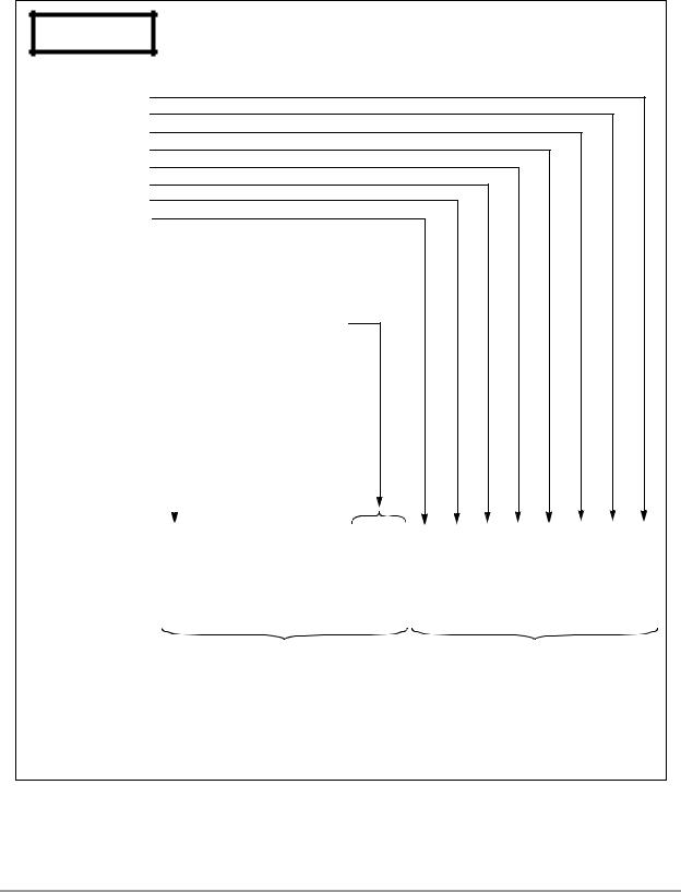
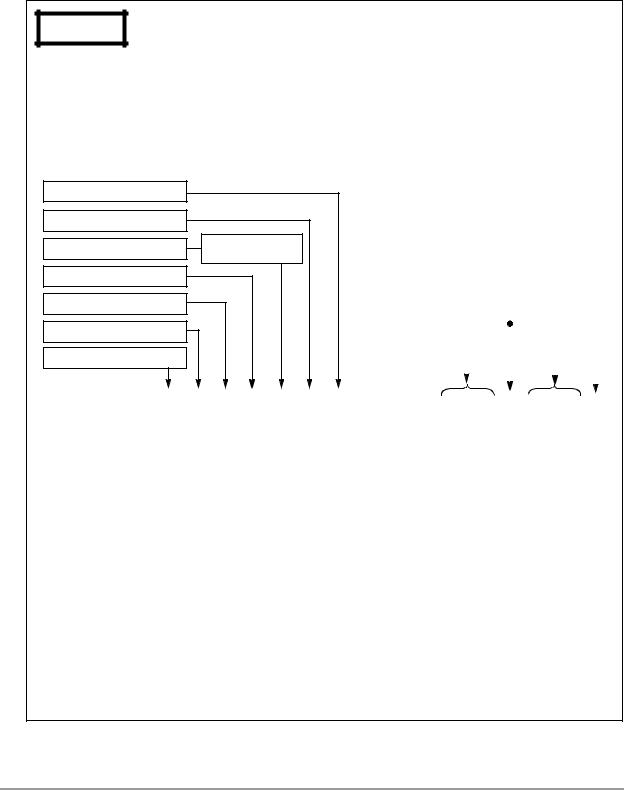
C.3 Programmer’s Sheets
The following pages provide programmer’s sheets that are intended to simplify programming the various registers in the DSP56824. The programmer’s sheets provide room to write in the value of each bit and the hexadecimal value for each register. The programmer can photocopy these sheets.
The programmer’s sheets are provided in the same order as the sections in this document. Table C-7 lists the sets of programmer’s sheets, the registers described in the sheets, and the pages in this appendix where the sheets are located.
Table C-7. List of Programmer’s Sheets
Type of |
Register |
Page |
|
Register |
|||
|
|
||
|
|
|
|
|
|
|
|
CPU |
JTAG instruction register |
C-13 |
|
|
|
|
|
|
JTAG bypass register |
C-13 |
|
|
|
|
|
|
JTAG ID register |
C-13 |
|
|
|
|
|
|
JTAG boundary scan register |
C-14 |
|
|
|
|
|
|
SR— Status register |
C-15 |
|
|
(includes mode register and condition code register) |
|
|
|
|
|
|
|
OMR— Operating mode register |
C-16 |
|
|
|
|
|
|
IPR— Interrupt priority register |
C-17 |
|
|
|
|
|
Memory |
BCR— Bus control register |
C-18 |
|
|
|
|
|
Port B GPIO |
PBINT— Port B interrupt register |
C-19 |
|
|
|
|
|
|
PBD— Port B data register |
C-19 |
|
|
|
|
|
|
PBINT— Port B data direction register |
C-19 |
|
|
|
|
|
Port C GPIO |
PCC— Port C control register |
C-20 |
|
|
|
|
|
|
PCD— Port C data register |
C-20 |
|
|
|
|
|
|
PCDDR— Port C data direction register |
C-20 |
|
|
|
|
|
SPI0 |
SPCR0— SPI 0 control register |
C-21 |
|
|
|
|
|
|
SPSR0— SPI 0 status register |
C-22 |
|
|
|
|
|
|
SPDR0— SPI 0 data register |
C-22 |
|
|
|
|
|
SPI1 |
SPCR1— SPI 1 control register |
C-23 |
|
|
|
|
|
|
SPCS1— SPI 1 status register |
C-24 |
|
|
|
|
|
|
SPDR1— SPI 1 data register |
C-24 |
|
|
|
|
Programmer’s Sheets |
C-11 |

Table C-7. List of Programmer’s Sheets (Continued)
Type of |
Register |
Page |
|
Register |
|||
|
|
||
|
|
|
|
|
|
|
|
SSI |
SCRRX— SSI receive control register |
C-25 |
|
|
|
|
|
|
SCRTX— SSI transmit control register |
C-25 |
|
|
|
|
|
|
SCR2— SSI control register 2 |
C-26 |
|
|
|
|
|
|
SCSR— SSI control/status register |
C-27 |
|
|
|
|
|
|
STSR— SSI time slot register |
C-28 |
|
|
|
|
|
|
STX— SSI transmit register |
C-28 |
|
|
|
|
|
|
STX— SSI receive register |
C-28 |
|
|
|
|
|
Timer 0 |
TCR01— Timer 0/1 control register |
C-29 |
|
|
|
|
|
|
TPR0— Timer 0 preload register |
C-29 |
|
|
|
|
|
|
TCT0— Timer 0 count register |
C-29 |
|
|
|
|
|
Timer 1 |
TCR01— Timer 0/1 control register |
C-30 |
|
|
|
|
|
|
TPR1— Timer 1 preload register |
C-30 |
|
|
|
|
|
|
TCT1— Timer 1 count register |
C-30 |
|
|
|
|
|
Timer 2 |
TCR2— Timer 2 control register |
C-31 |
|
|
|
|
|
|
TPR2— Timer 2 preload register |
C-31 |
|
|
|
|
|
|
TCT2— Timer 2 count register |
C-31 |
|
|
|
|
|
PLL |
PCR1— PLL control register 1 |
C-32 |
|
|
|
|
|
|
PCR0— PLL control register 0 |
C-32 |
|
|
|
|
|
COP/RTI |
COPCTL— COP control register |
C-33 |
|
|
|
|
|
|
COPCNT— COP count register |
C-33 |
|
|
|
|
C-12 |
DSP56824 User’s Manual |
|

Application: |
|
Date: |
|
|
|
|
Programmer: |
||
|
|
|
|
Sheet 1 of 6 |
CPU |
|
|
|
|
|
|
|
|
|
|
|
|
3 |
2 |
1 |
0 |
|
|
|
|
|
|
|
|
|
|
|
0 |
|||||
|
|
|
|
|
JTAG Instruction |
|
|
|
|
JTAG Bypass |
|
||||||||||||||||||||||
|
|
|
|
|
|
|
|
|
|
|
|
|
|
|
|
|
|
|
|||||||||||||||
|
|
|
|
|
|
B3 |
|
B2 |
|
|
B1 |
|
B0 |
|
|
|
|
|
|||||||||||||||
|
|
|
|
|
|
|
|
|
|
|
|
|
|
|
|
|
|
|
|
||||||||||||||
|
|
|
|
|
|
|
|
|
|
Register |
|
|
|
|
|
|
|
|
|
|
|
|
|
|
|
|
Register |
|
|
||||
|
|
|
|
|
|
|
|
Reset = $2 |
|
|
|
|
|
|
|
|
|
|
|
|
|
|
|
Reset = $0 |
|
|
|||||||
|
|
|
|
|
|
|
|
|
|
|
|
|
|
|
|
|
|
|
|
|
|
|
|
||||||||||
|
|
|
|
|
|
|
|
Read/Write |
|
|
|
|
|
|
|
|
|
|
|
|
|
|
|
Read/Write |
|
|
|||||||
|
|
|
|
|
|
|
|
|
|
|
|
|
|
|
|
|
|
|
|
|
|
|
|
|
|
|
|
|
|
|
|||
|
|
31 |
30 |
|
29 |
28 |
|
27 |
26 |
|
25 |
24 |
|
23 |
22 |
|
21 |
20 |
|
19 |
18 |
17 |
|
16 |
|||||||||
|
|
|
|
|
|
|
|
|
|||||||||||||||||||||||||
JTAG ID Register |
VER |
VER |
|
VER |
|
VER |
|
PNUM |
PNUM |
PNUM |
PNUM |
|
PNUM |
PNUM |
PNUM |
PNUM |
|
PNUM |
PNUM |
PNUM |
PNUM |
||||||||||||
3 |
2 |
|
1 |
|
|
0 |
|
15 |
14 |
|
13 |
12 |
|
11 |
10 |
|
9 |
8 |
|
7 |
6 |
|
5 |
|
4 |
||||||||
Read-Only |
|
|
|
|
|
|
|
|
|
|
|
|
|
|
|
|
|
|
|
|
|
|
|
|
|
|
|
|
|
|
|
|
|
|
|
|
|
|
|
|
|
|
|
|
|
|
|
|
|
|
|
|
|
|
|
|
|
|
|
|
|
|
|
|
|
|
|
|
|
|
|
|
|
|
|
|
|
|
1 |
|
|
|
|
|
|
|
5 |
|
|
|
|
|
|
|
0 |
|
|
||||
|
|
|
|
|
|
|
|
|
|
|
|
|
|
|
|
|
|
|
|
|
|
|
|
|
|
|
|||||||
|
|
15 |
14 |
|
13 |
12 |
|
11 |
10 |
|
9 |
8 |
|
7 |
6 |
|
5 |
4 |
|
3 |
2 |
1 |
|
0 |
|||||||||
|
|
|
|
|
|||||||||||||||||||||||||||||
|
|
PNUM |
PNUM |
PNUM |
PNUM |
|
MFG |
MFG |
|
MFG |
MFG |
|
MFG |
MFG |
|
MFG |
MFG |
|
MFG |
MFG |
|
MFG |
MFG |
||||||||||
|
|
3 |
2 |
|
1 |
|
|
0 |
|
ID11 |
ID10 |
|
|
ID9 |
|
ID8 |
|
|
ID7 |
|
ID6 |
|
|
ID5 |
ID4 |
|
ID3 |
ID2 |
|
ID1 |
ID0 |
||
|
|
|
|
|
|
|
|
|
|
|
|
|
|
|
|
|
|
|
|
|
|
|
|
|
|
|
|
|
|
|
|
|
|
|
|
|
2 |
|
|
|
|
|
|
0 |
|
|
|
|
|
|
|
1 |
|
|
|
|
|
|
|
D |
|
||||||
|
|
|
|
|
|
|
|
|
|
|
|
|
|
|
|
|
|
|
|
|
|
|
|
|
|
|
|
|
|
|
|
|
|
|
|
|
|
|
|
|
|
|
|
|
|
|
|
|
|
|
|
|
|
|
|
|
|
|
|
|
|
|
|
||||
|
|
Bitfield |
|
|
|
|
|
|
|
|
|
Usage |
|
|
|
|
|
|
|
|
|
|
|
|
|
|
|
|
|
||||
|
|
|
|
|
|
|
|
|
|
|
|
|
|
|
|||||||||||||||||||
|
|
|
|
|
|
|
|
|
|
|
|
|
|
|
|||||||||||||||||||
|
|
VER[3:0] |
|
|
Version number of chip mask (varies with mask) |
|
|
|
|
|
|
|
|
|
|||||||||||||||||||
|
|
|
|
|
|
|
|
|
|
|
|
|
|
|
|||||||||||||||||||
|
|
PNUM[15:0] |
|
|
Customer part number (specifies DSP56824) |
|
|
|
|
|
|
|
|
|
|||||||||||||||||||
|
|
|
|
|
|
|
|
|
|
|
|
|
|
|
|
|
|
|
|
|
|
||||||||||||
|
|
MFG ID[11:0] |
|
Specifies manufacturer identity |
|
|
|
|
|
|
|
|
|
|
|
|
|
|
|
|
|
||||||||||||
|
|
|
|
|
|
|
|
|
|
|
|
|
|
|
|
|
|
|
|
|
|
|
|
|
|
|
|
|
|
|
|
|
|
Programmer’s Sheets |
C-13 |

Application: |
|
|
|
|
|
|
|
|
|
|
|
|
|
|
|
|
|
|
Date: |
|
|
|
|
|
|
|
|
|
||
|
|
|
|
|
|
|
|
|
|
|
|
|
|
|
|
|
|
|
|
Programmer: |
|
|
|
|
|
|
||||
|
|
|
|
|
|
|
|
|
|
|
|
|
|
|
|
|
|
|
|
|
|
|
|
|
|
Sheet 2 of 6 |
||||
|
|
|
|
|
|
|
|
|
|
|
|
|
|
|
|
|
|
|
|
|
|
|
|
|
|
|
|
|
|
|
|
|
|
|
|
|
|
|
|
|
|
|
|
|
|
|
|
|
|
|
|
|
|
|
|
|
|
||||
|
CPU |
|
110 |
109 |
108 |
|
|
|
107 |
106 |
105 |
104 |
|
103 |
102 |
101 |
100 |
|
99 |
98 |
97 |
96 |
|
|
||||||
|
|
|
|
|||||||||||||||||||||||||||
|
|
|
|
|
RE |
|
MODB/ |
MODA/ |
|
|
PB0 |
PB0 |
PB1 |
PB1 |
|
PB2 |
PB2 |
PB3 |
PB3 |
|
PB4 |
|
PB4 |
PB5 |
PB5 |
|
|
|||
|
JTAG Boundary Scan |
|
SET |
IRQB |
IRQA |
|
|
ctrl |
|
ctrl |
|
|
ctrl |
|
|
ctrl |
|
|
|
ctrl |
|
|
ctrl |
|
|
|
||||
|
|
Register |
|
|
|
|
|
|
|
|
|
|
|
|
|
|
|
|
|
|
|
|
|
|
|
|
|
|
|
|
|
|
|
|
|
|
|
|
|
|
|
|
|
|
|
|
|
|
|
|
|
|
|
|
|
|
|
|
|
||
|
|
Read-Only |
|
|
|
|
|
|
|
|
|
|
|
|
|
|
|
|
|
|
|
|
|
|
|
|
|
|
|
|
95 |
|
|
|
|
|
|
|
|
|
|
|
|
|
|
|
|
|
|
|
|
|
|
|
|
|
|
|
|||
94 |
|
93 |
92 |
|
|
91 |
90 |
89 |
88 |
|
87 |
86 |
85 |
84 |
|
83 |
82 |
81 |
80 |
|
|
|||||||||
|
|
|
|
|||||||||||||||||||||||||||
|
|
|
|
|
|
|
|
|
|
|
|
|
|
|
|
|
|
|
|
|
|
|
|
|
||||||
|
|
|
PB6 |
|
PB6 |
PB7 |
PB7 |
|
|
|
PB8 |
PB8 |
PB9 |
PB9 |
|
PB10 |
PB10 |
PB11 |
PB11 |
|
PB12 |
PB12 |
PB13 |
PB13 |
|
|||||
|
|
|
ctrl |
|
|
|
ctrl |
|
|
|
|
ctrl |
|
ctrl |
|
|
ctrl |
|
|
ctrl |
|
|
|
ctrl |
|
|
ctrl |
|
|
|
|
|
|
|
|
|
|
|
|
|
|
|
|
|
|
|
|
|
|
|
|
|
|
|
|
|
|
|
|
|
|
|
|
|
|
|
|
|
|
|
|
|
|
|
|
|
|
|
|
|
|
|
|
|
|
|
|
|
|
|
|
|
79 |
78 |
77 |
76 |
|
75 |
74 |
73 |
72 |
|
71 |
70 |
69 |
68 |
|
67 |
66 |
65 |
64 |
|
|
|
||||||||||||||||
PB14 |
PB14 |
PB15 |
PB15 |
|
CLKO |
EX |
PC0 |
PC0 |
|
PC1/ |
PC1/ |
PC2/ |
PC2/ |
|
PC3/ |
PC3/ |
PC4/ |
PC4/ |
ctrl |
|
ctrl |
|
|
|
|
MISO0 |
MISO0 |
|
MOSI0 |
MOSI0 |
SCK0 |
SCK0 |
|
SS0 |
SS0 |
MISO1 |
MISO1 |
|
|
|
|
|
|
|
ctrl |
|
|
ctrl |
|
ctrl |
|
|
ctrl |
|
ctrl |
|
|
|
|
|
|
|
|
|
|
|
|
|
|
|
|
|
|
|
|
|
|
|
|
|
|
|
|
|
|
|
|
|
|
|
|
|
|
|
63 |
62 |
61 |
60 |
|
59 |
58 |
57 |
56 |
|
55 |
54 |
53 |
52 |
|
51 |
50 |
49 |
48 |
|
|
|
||||||||||||||||
PC5/ |
PC5/ |
PC6/ |
PC6/ |
|
PC7/ |
PC7/ |
PC8/ |
PC8 |
|
PC9/ |
PC9/ |
PC10/ |
PC10/ |
|
PC11/ |
PC11/ |
PC12/ |
PC12/ |
MOSI1 |
MOSI1 |
SCK1 |
SCK1 |
|
SS1 |
SS1 |
STD |
STD |
|
SRD |
SRD |
STCK |
STCK |
|
STFS |
STFS |
SRCK |
SRCK |
ctrl |
|
ctrl |
|
|
ctrl |
|
ctrl |
|
|
ctrl |
|
ctrl |
|
|
ctrl |
|
ctrl |
|
|
|
|
|
|
|
|
|
|
|
|
|
|
|
|
|
|
|
|
|
|
|
|
|
|
|
|
|
|
|
|
|
|
|
|
|
|
|
47 |
46 |
45 |
44 |
|
43 |
42 |
41 |
|
40 |
|
|
39 |
38 |
37 |
36 |
|
35 |
34 |
33 |
32 |
||||||
|
|
|
||||||||||||||||||||||||
PC13/ |
PC13/ |
PC14/ |
PC14/ |
|
PC15/ |
PC15/ |
|
WR |
|
WR |
|
|
RD |
|
RD |
A15 |
A15 |
|
A14 |
A13 |
A12 |
A11 |
||||
SRFS |
SRFS |
TIO01 |
TIO01 |
|
TIO2 |
TIO2 |
|
ctrl |
|
|
|
|
|
ctrl |
|
|
|
ctrl |
|
|
|
|
|
|
||
ctrl |
|
ctrl |
|
|
ctrl |
|
|
|
|
|
|
|
|
|
|
|
|
|
|
|
|
|
|
|
|
|
|
|
|
|
|
|
|
|
|
|
|
|
|
|
|
|
|
|
|
|
|
|
|
|
|
|
|
|
|
|
|
|
|
|
|
|
|
|
|
|
|
|
|
|
|
|
|
|
|
|
|
|
|
|
31 |
30 |
29 |
28 |
|
27 |
26 |
25 |
24 |
|
23 |
22 |
21 |
20 |
|
19 |
18 |
17 |
16 |
||||||||
|
|
|
||||||||||||||||||||||||
A10 |
A9 |
A8 |
A7 |
|
A6 |
A5 |
|
PS |
|
PS |
|
|
DS |
|
DS |
A4 |
A3 |
|
A2 |
A1 |
A0 |
D0 |
||||
|
|
|
|
|
|
|
|
ctrl |
|
|
|
|
|
ctrl |
|
|
|
|
|
|
|
|
|
|
||
|
|
|
|
|
|
|
|
|
|
|
|
|
|
|
|
|
|
|
|
|
|
|
|
|
|
|
|
|
|
|
|
|
|
|
|
|
|
|
|
|
|
|
|
|
|
|
|
|
|
|
|
|
|
15 |
14 |
13 |
12 |
|
11 |
10 |
9 |
8 |
|
7 |
6 |
5 |
4 |
|
3 |
2 |
1 |
0 |
|
|
|
||||||||||||||||
D1 |
D2 |
D3 |
D4 |
|
D5 |
D6 |
D7 |
D8 |
|
D9 |
D10 |
D11 |
D12 |
|
D13 |
D14 |
D15 |
D15 |
|
|
|
|
|
|
|
|
|
|
ctrl |
|
|
|
|
|
|
ctrl |
|
|
|
|
|
|
|
|
|
|
|
|
|
|
|
|
|
|
|
|
|
|
|
|
|
|
|
|
|
|
|
|
|
|
|
|
|
|
|
C-14 |
DSP56824 User’s Manual |
|
Application: |
|
Date: |
|
|
|
|
Programmer: |
|
|
Sheet 3 of 6
CPU
Carry
Overflow
Zero
Negative
Unnormalized
Extension
Limit
Size
I1 |
I0 |
Exceptions Permitted |
Exceptions Masked |
|
|
|
|
0 |
0 |
(Reserved) |
(Reserved) |
|
|
|
|
0 |
1 |
IPL0, IPL1 |
None |
|
|
|
|
1 |
0 |
(Reserved) |
(Reserved) |
|
|
|
|
1 |
1 |
IPL1 |
IPL0 |
|
|
|
|
LF |
|
Exceptions Masked |
|
|
|
|
|
|
|
|
|
|
|
|
|
|
|
|
|
|
|
||
|
|
|
|
|
|
|
|
|
|
|
|
|
|
|
|
|
|
|
|
|
|
||
0 |
|
Loop not running |
|
|
|
|
|
|
|
|
|
|
|
|
|
|
|
|
|
|
|
||
|
|
|
|
|
|
|
|
|
|
|
|
|
|
|
|
|
|
|
|
|
|
||
1 |
|
Loop is running |
|
|
|
|
|
|
|
|
|
|
|
|
|
|
|
|
|
|
|
||
|
|
|
|
|
|
|
|
|
|
|
|
|
|
|
|
|
|
|
|
|
|
|
|
|
|
|
|
|
|
|
|
|
|
|
|
|
|
|
|
|
|
|
|
|
|
|
|
|
15 |
14 |
13 |
12 |
|
11 |
10 |
9 |
8 |
|
7 |
6 |
5 |
4 |
|
3 |
2 |
1 |
0 |
||||
|
|
|
|
||||||||||||||||||||
Status Register |
|
|
|
|
|
|
|
|
|
|
|
|
|
|
|
|
|
|
|
|
|||
LF |
* |
* |
* |
|
* |
* |
I1 |
I0 |
|
S |
L |
E |
U |
|
N |
Z |
V |
C |
|||||
|
|
(SR) |
|
|
|
|
|
|
|
|
|
|
|
|
|
|
|
||||||
|
|
|
0 |
0 |
0 |
|
0 |
0 |
|
|
|
|
|
|
|
|
|
|
|
|
|||
|
Reset = $0300 |
|
|
|
|
|
|
|
|
|
|
|
|
|
|
|
|||||||
|
|
|
|
|
|
|
|
|
|
|
|
|
|
|
|
|
|
|
|
|
|||
|
|
Read/Write |
|
|
|
|
|
|
|
|
|
|
|
|
|
|
|
|
|
|
|
|
|
|
|
|
|
|
|
|
|
|
|
|
|
|
|
|
|
|
|
|
|
|
|
|
|
MR |
CCR |
Mode Register |
Condition Code Register |
* = Reserved, program as zero |
|
Programmer’s Sheets |
C-15 |
Application: |
|
|
Date: |
|
|
|
|
|
Programmer: |
||
|
|
|
|
|
Sheet 4 of 6 |
|
|
CPU |
|
|
|
|
|
|
|
|
|
|
|
|
|
|
|
|
|
|
|
|
|
|
|
|
MB |
|
MA |
|
|
Description |
|||||
|
|
|
|
|
|
|
|
|
|
|
|
|
||||||
|
|
|
|
|
|
|
|
|
|
|
|
|
|
|
|
|
|
|
|
|
|
|
|
|
|
|
|
|
|
|
|
|
|
|
|
|
|
|
|
|
|
|
|
|
|
|
|
0 |
|
0 |
Mode 0— Single Chip |
|||||
|
|
|
|
|
|
|
|
|
|
|
|
|
|
|
|
|
|
|
|
|
|
|
|
|
|
|
|
|
0 |
|
1 |
(Reserved) |
|||||
|
|
|
|
|
|
|
|
|
|
|
|
|
|
|
|
|
|
|
|
|
|
|
|
|
|
|
|
|
1 |
|
0 |
Mode 2— Normal Expanded |
|||||
|
|
|
|
|
|
|
|
|
|
|
|
|
|
|
|
|
|
|
|
|
|
|
|
|
|
|
|
|
1 |
|
1 |
Mode 3— Development |
|||||
|
|
|
|
|
|
|
|
|
|
|
|
|
|
|
|
|
|
|
|
|
|
|
|
|
|
|
|
|
|
|
|
|
|
|
|
|
|
|
|
|
|
|
|
|
|
|
|
EX |
|
|
|
Description |
|
|||
|
|
|
|
|
|
|
|
|
|
|
|
|
|
|
||||
|
|
|
|
|
|
|
|
|
|
|
|
|
|
|
||||
|
|
|
|
|
|
|
|
|
|
0 |
External X memory disabled |
|
||||||
|
|
|
|
|
|
|
|
|
|
|
|
|
|
|
||||
|
|
|
|
|
|
|
|
|
|
1 |
External X memory enabled |
|
||||||
|
|
|
|
|
|
|
|
|
|
|
|
|
|
|
|
|
||
|
|
|
|
|
|
|
|
|
|
|
|
|
|
|
|
|||
|
|
|
|
|
|
|
|
|
SA |
|
|
|
Description |
|
|
|||
|
|
|
|
|
|
|
|
|
|
|
|
|
||||||
|
|
|
|
|
|
|
|
|
|
|
|
|
|
|||||
|
|
|
|
|
|
|
|
|
0 |
Saturation mode disabled |
|
|
||||||
|
|
|
|
|
|
|
|
|
|
|
|
|
||||||
|
|
|
|
|
|
|
|
|
1 |
Saturation mode enabled |
|
|
||||||
|
|
NL |
Description |
|
|
|
|
|
|
|
|
|
|
|
|
|
||
|
|
|
|
|
|
|
|
|
|
|
|
|
|
|
|
|||
|
|
|
|
|
|
|
|
|
|
|
|
|
|
|
|
|||
|
0 |
Nested loop not executing |
|
|
|
|
|
|
|
|
|
|
|
|
|
|||
|
1 |
Nested loop is executing |
|
R |
|
|
Description |
|
|
|
|
|
||||||
|
|
|
|
|
|
|
|
|
|
|
|
|
|
|||||
|
|
|
|
|
|
|
|
|
|
|
|
|
||||||
|
|
|
|
|
|
|
0 |
Convergent rounding used |
|
|
|
|||||||
|
|
|
|
|
|
|
|
|
|
|||||||||
|
|
|
|
|
|
|
|
|
|
|||||||||
|
|
|
|
|
|
|
1 |
Two’s-complement rounding used |
|
|
|
|||||||
|
|
|
|
|
|
|
|
|
|
|
|
|
|
|
|
|
||
|
|
|
|
|
|
|
|
|
|
|
|
|
|
|
|
|
|
|
|
|
|
|
|
|
|
SD |
|
Description |
|
|
|
|
|
||||
|
|
|
|
|
|
|
|
|
|
|
|
|
|
|
|
|
||
|
|
|
|
|
|
|
|
|
|
|
|
|
|
|
|
|
||
|
|
|
|
|
|
|
0 |
Stop delay enabled |
|
|
|
|
|
|||||
|
|
|
|
|
|
|
|
|
|
|
|
|
|
|
|
|
||
|
|
|
|
|
|
|
1 |
Stop delay disabled |
|
|
|
|
|
|||||
|
|
|
|
|
|
|
|
|
|
|
|
|
|
|
|
|
|
|
|
|
|
|
|
|
|
|
|
|
|
|
|
|
|
|
|
|
|
|
|
|
|
|
CC |
Description |
|
|
|
|
|
|
|
|
|
|||
0Condition codes generated based on 36-bit MAC result
1Condition codes generated based
|
|
|
on 32-bit MAC result |
|
|
|
|
|
|
|
|
|
|
|
|
|
|||||
|
|
|
|
|
|
|
|
|
|
|
|
|
|
|
|
|
|
|
|
|
|
15 |
14 |
13 |
12 |
|
11 |
|
10 |
9 |
8 |
|
7 |
6 |
5 |
4 |
|
3 |
2 |
1 |
0 |
||
|
|
|
|||||||||||||||||||
Operating Mode |
|
|
|
|
|
|
|
|
|
|
|
|
|
|
|
|
|
|
|
|
|
NL |
* |
* |
* |
|
* |
|
* |
* |
CC |
|
* |
SD |
R |
SA |
|
EX |
* |
MB |
MA |
||
Register (OMR) |
|
|
|
|
|
|
|
|
|
|
|
|
|
||||||||
|
0 |
0 |
0 |
|
0 |
|
0 |
0 |
|
|
|
0 |
|
|
|
|
|
0 |
|
|
|
Reset = $0000 |
|
|
|
|
|
|
|
|
|
|
|
|
|
||||||||
|
|
|
|
|
|
|
|
|
|
|
|
|
|
|
|
|
|
|
|
|
|
|
|
|
|
|
|
|
|
|
|
|
|
|
|
|
|
|
|
|
|
|
|
Read/Write |
|
|
|
|
|
|
|
|
|
|
|
|
|
|
|
|
|
|
|
|
|
|
|
|
|
|
|
|
|
|
|
|
|
|
|
|
|
|
|
|
|
|
|
|
* = Reserved, program as zero |
|
|
|
|
|
|
|
|
|
|
|
|
|
|
||||||
C-16 |
DSP56824 User’s Manual |
|
Application: |
|
|
Date: |
|
|
|
|
|
Programmer: |
|
|
Sheet 5 of 6
CPU
IBL1 |
IBL0 |
IRQ B Mode |
|
|
|
|
|
|
|
|
|
|
|
|
0 |
0 |
IRQ B disabled |
|
|
|
|
|
|
|
0 |
1 |
IRQ B enabled, level-sensitive trigger |
|
|
|
|
|
|
|
1 |
0 |
IRQ B disabled |
|
|
|
|
|
|
|
1 |
1 |
IRQ B enabled, edge-sensitive trigger |
|
|
|
|
|
|
|
Channel 6 IPL
Channel 5 IPL
Channel 4 IPL
Channel 3 IPL
Channel 2 IPL
Channel 1 IPL
Channel 0 IPL
Set to 1 to Enable Interrupt Channels
|
IAL1 |
IAL0 |
|
IRQ A Mode |
|
|
|
|
|||
|
|
|
|
|
|
|
|
|
|
|
|
|
|
|
|
|
|
|
|
|
|
|
|
|
0 |
|
0 |
|
IRQ A disabled |
||||||
|
|
|
|
|
|
|
|
|
|
|
|
|
0 |
|
1 |
|
IRQ A enabled, level-sensitive trigger |
||||||
|
|
|
|
|
|
|
|
|
|
|
|
|
1 |
|
0 |
|
IRQ A disabled |
||||||
|
|
|
|
|
|
|
|
|
|
|
|
|
1 |
|
1 |
|
IRQ A enabled, edge-sensitive trigger |
||||||
|
|
|
|
|
|
|
|
|
|
|
|
|
|
|
|
|
|
|
|
|
|
|
|
|
|
|
|
IxL1 |
IxINV |
Trigger Mode |
|||||
|
|
|
|
|
|
|
|
|
|
|
|
|
|
|
|
|
|
|
|
|
|
|
|
|
|
|
|
0 |
0 |
Low-level sensitive |
|||||
|
|
|
|
|
|
|
|
|
|
|
|
|
|
|
|
0 |
1 |
High-level sensitive |
|||||
|
|
|
|
|
|
|
|
|
|
|
|
|
|
|
|
1 |
0 |
Falling-edge sensitive |
|||||
|
|
|
|
|
|
|
|
|
|
|
|
|
|
|
|
1 |
1 |
Rising-edge sensitive |
|||||
|
|
|
|
|
|
|
|
|
|
|
|
|
|
|
|
|
|
|
|
|
|
|
|
|
|
|
|
|
|
|
|
|
|
|
|
|
|
|
|
|
|
|
|
|
|
|
|
|
|
|
|
|
|
|
|
|
|
|
|
|
|
|
|
|
|
|
|
|
|
|
|
|
|
|
|
|
|
|
|
|
|
|
|
15 |
14 |
13 |
12 |
|
|
|
11 |
10 |
|
9 |
8 |
|
7 |
6 |
5 |
4 |
|
3 |
2 |
1 |
0 |
||
|
|
|
|||||||||||||||||||||
Interrupt Priority |
CH0 |
CH1 |
CH2 |
CH3 |
|
|
CH4 |
CH5 |
|
CH6 |
* |
|
* |
* |
IBL1 |
IBL0 |
|
IB |
IAL1 |
IAL0 |
IA |
||
Register (IPR) |
|
|
|
|
|
|
|
|
|
|
|
0 |
|
0 |
0 |
|
|
|
INV |
|
|
INV |
|
|
|
|
|
|
|
|
|
|
|
|
|
|
|
|
|
|
|
|
|||||
X:$FFFB |
|
|
|
|
|
|
|
|
|
|
|
|
|
|
|
|
|
|
|
||||
|
|
|
|
|
|
|
|
|
|
|
|
|
|
|
|
|
|
|
|
|
|
|
|
|
|
|
|
|
|
|
|
|
|
|
|
|
|
|
|
|
|
|
|
|
|
|
|
Reset = $0000 |
|
|
|
|
|
|
|
|
|
|
|
|
|
|
|
|
|
|
|
|
|
|
|
|
|
|
|
|
|
|
|
|
|
|
|
|
|
|
|
|
|
|
|
|
|
|
|
|
* = Reserved, Program as 0 |
|
|
|
|
|
|
|
|
|
|
|
|
|
|
|
|||||||
|
|
|
|
|
|
|
|
|
|
|
|
|
|
|
|||||||||
|
Interrupt Channel |
|
Associated Peripheral |
|
|
|
|
|
|
|
|
|
|
|
|||||||||
|
|
|
|
|
|
|
|
|
|
|
|
|
|
|
|
|
|
|
|
|
|
||
|
|
|
|
|
|
|
|
|
|
|
|
|
|
|
|
|
|
|
|
|
|
||
|
|
6 |
|
|
|
SSI |
|
|
|
|
|
|
|
|
|
|
|
|
|
|
|
||
|
|
|
|
|
|
|
|
|
|
|
|
|
|
|
|
|
|
|
|
||||
|
|
5 |
|
|
|
(Reserved) |
|
|
|
|
|
|
|
|
|
|
|
|
|
||||
|
|
|
|
|
|
|
|
|
|
|
|
|
|
|
|
|
|
|
|
||||
|
|
4 |
|
|
|
Timer module |
|
|
|
|
|
|
|
|
|
|
|
|
|
||||
|
|
|
|
|
|
|
|
|
|
|
|
|
|
|
|
|
|
|
|
|
|
||
|
|
3 |
|
|
|
SPI1 |
|
|
|
|
|
|
|
|
|
|
|
|
|
|
|
||
|
|
|
|
|
|
|
|
|
|
|
|
|
|
|
|
|
|
|
|
|
|
||
|
|
2 |
|
|
|
SPI0 |
|
|
|
|
|
|
|
|
|
|
|
|
|
|
|
||
|
|
|
|
|
|
|
|
|
|
|
|
|
|
|
|
|
|
|
|||||
|
|
1 |
|
|
|
Real-time timer |
|
|
|
|
|
|
|
|
|
|
|
|
|||||
|
|
|
|
|
|
|
|
|
|
|
|
|
|
|
|
|
|
|
|
||||
|
|
0 |
|
|
|
Port B GPIO |
|
|
|
|
|
|
|
|
|
|
|
|
|
||||
|
|
|
|
|
|
|
|
|
|
|
|
|
|
|
|
|
|
|
|
|
|
|
|
Programmer’s Sheets |
C-17 |
Application: |
|
|
|
|
|
|
|
|
|
|
|
|
|
|
|
|
|
|
|
|
|
|
|
Date: |
|
|
|
|
|
|
|
|
|
|
|
|
||
|
|
|
|
|
|
|
|
|
|
|
|
|
|
|
|
|
|
|
|
|
|
|
|
|
Programmer: |
|
|
|
|
|
|
|
|
|||||
|
|
|
|
|
|
|
|
|
|
|
|
|
|
|
|
|
|
|
|
|
|
|
|
|
|
|
|
|
|
|
|
Sheet 6 of 6 |
||||||
|
|
|
|
|
|
|
|
|
|
|
|
|
|
|
|
|
|
|
|
|
|
|
|
|
|
|
|
|
|
|
|
|
|
|
|
|||
|
|
|
|
|
|
|
|
|
|
|
|
|
|
|
|
|
|
|
|
|
|
|
|
|
|
|
|
|
|
|
|
|
|
|
|
|||
|
CPU |
|
|
|
|
|
|
|
|
|
|
|
|
|
|
|
|
|
|
|
|
|
|
Wait state field for external |
|
|
|
|
|
|||||||||
|
|
|
|
|
|
|
|
|
|
|
|
|
|
|
|
|
|
|
|
|
|
|
|
X (data) memory |
|
|
|
|
|
|||||||||
|
|
|
|
|
|
|
|
|
|
|
|
|
|
|
|
|
|
|
|
|
|
|
|
|
|
|
|
|
|
|
|
|
|
|
|
|
|
|
|
|
|
|
|
|
|
|
|
|
|
|
|
|
|
|
|
|
|
|
|
|
|
|
|
|
|
|
|
|
|
|
|
|
|||||
|
|
|
DRV |
|
|
|
Description |
|
|
|
|
|
|
|
|
|
|
|
|
|
|
|
|
|
|
|
|
|
|
|
|
|
|
|||||
|
|
|
|
0 |
Port A pins are tri-stated |
|
|
|
|
|
|
|
|
|
|
|
Wait state field for external |
|
|
|||||||||||||||||||
|
|
|
|
|
|
|
|
|
|
|
|
|
|
|
P (program) memory |
|
|
|
|
|
||||||||||||||||||
|
|
|
|
|
|
|
|
|
|
|
|
|
|
|
|
|
|
|
|
|
|
|
|
|
|
|
|
|
|
|
||||||||
|
|
|
|
1 |
Port A pins remain driven |
|
|
|
|
|
|
|
|
|
|
|
|
|
|
|
|
|
|
|
|
|
|
|
|
|||||||||
|
|
|
|
|
|
|
|
|
|
|
|
|
|
|
|
|
|
|
|
|
|
|
|
|
|
|
|
|||||||||||
|
|
|
|
|
|
|
|
|
|
|
|
|
|
|
|
|
|
|
|
|
|
|
|
|
|
|
|
|
|
|
|
|
|
|
|
|
|
|
|
|
|
|
|
|
|
|
|
|
|
|
|
|
|
|
|
|
|
|
|
|
|
|
|
|
|
|
|
|
|
|
|
|
|
|
|
|
|
|
|
|
|
15 |
14 |
13 |
12 |
|
|
11 |
|
10 |
9 |
8 |
|
7 |
6 |
|
5 |
4 |
|
|
3 |
|
2 |
1 |
0 |
|
|
|
|
|||||||
|
|
|
|
|
|
|
|
|
|
|||||||||||||||||||||||||||||
|
|
|
|
|
|
|
|
|
|
|
|
|
|
|
|
|
|
|
|
|
|
|
|
|
|
|
|
|
|
|
||||||||
|
Bus Control |
|
* |
|
* |
|
* |
* |
|
|
* |
|
* |
DRV |
* |
|
WSX3 |
WSX2 |
WSX1 |
WSX0 |
|
WSP3 |
WSP2 |
WSP1 |
WSP0 |
|
||||||||||||
|
|
|
|
|
|
|
|
|
|
|
|
|
|
|
|
|
|
|
|
|
|
|
|
|
|
|
|
|||||||||||
|
Register (BCR) |
|
0 |
|
0 |
|
0 |
0 |
|
|
0 |
|
0 |
|
|
0 |
|
|
|
|
|
|
|
|
|
|
|
|
|
|
|
|
|
|
|
|||
|
X:$FFF9 |
|
|
|
|
|
|
|
|
|
|
|
|
|
|
|
|
|
|
|
|
|
|
|
|
|
|
|
|
|
|
|
|
|
|
|
||
|
|
|
|
|
|
|
|
|
|
|
|
|
|
|
|
|
|
|
|
|
|
|
|
|
|
|
|
|
|
|
|
|
|
|
|
|||
|
Reset = $00FF |
|
|
|
|
$0 |
|
|
|
|
|
|
|
|
|
|
|
|
|
|
|
|
|
|
|
|
|
|
|
|
|
|
|
|
|
|||
|
|
|
|
|
|
|
|
|
|
|
|
|
|
|
|
|
|
|
|
|
|
|
|
|
|
|
|
|
|
|
|
|
|
|
|
|
|
|
* = Reserved, program as zero
C-18 |
DSP56824 User’s Manual |
|
Application: |
|
|
Date: |
|
|
|
|
|
Programmer: |
|
|
Sheet 1 of 1
Port B |
|
|
|
|
|
|
|
|
|
|
|
|
|
|
|
|
|
|
|
|
|
|
|
|
|
|
|
|
|
|
|
|
|
|
|
|
|
|
|
|
|
INVn |
|
Description |
|
|
|
||||||
|
|
|
|
|
|
|
|
|
|
|
|
|
|
|
|
|
|
|
|
|
||||||
GPIO |
|
|
|
|
|
|
|
|
|
|
|
|
|
|
|
|
|
|
|
|
|
|
|
|
||
|
|
|
|
|
|
|
|
|
|
|
|
|
|
|
|
|
|
|
|
|
|
|
|
|||
|
|
|
|
|
|
|
|
|
|
|
|
|
|
|
0 |
Detects rising edge |
|
|
|
|||||||
|
|
|
|
|
|
|
|
|
|
|
|
|
|
|
|
|
|
|
|
|
|
|
|
|||
|
|
|
|
|
|
|
|
|
|
|
|
|
|
|
1 |
Detects falling edge |
|
|
|
|||||||
|
|
|
|
|
|
|
|
|
|
|
|
|
|
|
|
|
|
|
|
|
|
|
|
|
|
|
|
|
MSKn |
|
|
|
Description |
|
|
|
|
|
|
|
|
|
|
|
|
|
|
|
|||||
|
|
|
|
|
|
|
|
|
|
|
|
|
|
|
|
|
|
|
|
|
|
|
|
|
|
|
|
0 |
|
Pin masked from generating interrupt |
|
|
|
|
|
|
|
|
|
|
|
|
|
|
|||||||||
|
|
|
|
|
|
|
|
|
|
|
|
|
|
|
|
|
|
|
|
|
|
|
|
|
|
|
|
1 |
|
Pin enabled for generating interrupt |
|
|
|
|
|
|
|
|
|
|
|
|
|
|
|||||||||
|
|
|
|
|
|
|
|
|
|
|
|
|
|
|
|
|
|
|
|
|
|
|
|
|
|
|
15 |
14 |
13 |
12 |
|
|
11 |
10 |
9 |
8 |
|
7 |
|
6 |
5 |
4 |
|
3 |
2 |
1 |
0 |
||||||
|
|
|
|
|
||||||||||||||||||||||
|
|
|
|
|||||||||||||||||||||||
Port B Interrupt |
MSK7 |
MSK6 |
MSK5 |
MSK4 |
|
MSK3 |
MSK2 |
MSK1 |
MSK0 |
|
INV7 |
|
INV6 |
INV5 |
INV4 |
INV3 |
INV2 |
INV1 |
INV0 |
|||||||
Register (PBINT) |
|
|
|
|
|
|
|
|
|
|
|
|
|
|
|
|
|
|
|
|
|
|
|
|
||
X:$FFEA |
|
|
|
|
|
|
|
|
|
|
|
|
|
|
|
|
|
|
|
|
|
|
|
|
||
|
|
|
|
|
|
|
|
|
|
|
|
|
|
|
|
|
|
|
|
|
|
|
|
|||
Reset = $0000 |
|
|
|
|
|
|
|
|
|
|
|
|
|
|
|
|
|
|
|
|
|
|
|
|
||
|
|
|
|
|
|
|
|
|
|
|
|
|
|
|
|
|
|
|
|
|
|
|
|
|
|
|
15 |
14 |
13 |
12 |
|
11 |
10 |
9 |
8 |
|
7 |
6 |
5 |
4 |
|
3 |
2 |
1 |
0 |
|
|
|
|
|||||||||||||||||
Port B Data |
BD15 |
BD14 |
BD13 |
BD12 |
|
BD11 |
BD10 |
BD9 |
BD8 |
|
BD7 |
BD6 |
BD5 |
BD4 |
|
BD3 |
BD2 |
BD1 |
BD0 |
Register (PBD) |
|
|
|
|
|
|
|
|
|
|
|
|
|
|
|
|
|
|
|
X:$FFEC |
|
|
|
|
|
|
|
|
|
|
|
|
|
|
|
|
|
|
|
|
|
|
|
|
|
|
|
|
|
|
|
|
|
|
|
|
|
|
|
Reset = Uninitialized |
|
|
|
|
|
|
|
|
|
|
|
|
|
|
|
|
|
|
|
|
|
|
|
|
|
|
|
|
|
|
|
|
|
|
|
|
|
|
|
15 |
14 |
13 |
12 |
|
11 |
10 |
9 |
8 |
|
7 |
6 |
5 |
4 |
|
3 |
2 |
1 |
0 |
|
|
|
|
|||||||||||||||||
Port B |
|
|
|
|
|
|
|
|
|
|
|
|
|
|
|
|
|
|
|
BDD15 |
BDD14 |
BDD13 |
BDD12 |
|
BDD11 |
BDD10 |
BDD9 |
BDD8 |
|
BDD7 |
BDD6 |
BDD5 |
BDD4 |
|
BDD3 |
BDD2 |
BDD1 |
BDD0 |
|
Data Direction |
|
|
|
|
|
|
|
|
|
|
|
|
|
|
|
|
|
|
|
Register (PBDDR) |
|
|
|
|
|
|
|
|
|
|
|
|
|
|
|
|
|
|
|
X:$FFEB |
|
|
|
|
|
|
|
|
|
|
|
|
|
|
|
|
|
|
|
Reset = $0000 |
|
|
|
|
|
|
|
|
|
|
|
|
|
|
|
|
|
|
|
|
|
|
|
|
|
|
|
|
|
|
|
|
|
|
|
|
|
|
|
Programmer’s Sheets |
C-19 |
Application: |
|
|
Date: |
|
|
|
|
|
Programmer: |
|
|
Sheet 1 of 1
Port C
GPIO
PCC register must be configured for Port C GPIO, Timers 0–2, SPI 0–1, and SSI. Use this programming sheet for all these peripherals.
Timer |
|
Synchronous Serial |
|
SPI1 |
|
SPI0 |
|
Interface (SSI) |
|
|
|||
|
|
|
|
|
|
|
|
|
|
|
|
|
|
15 |
14 |
13 |
12 |
|
11 |
10 |
9 |
8 |
|
7 |
6 |
|
5 |
4 |
|
3 |
2 |
1 |
0 |
||
|
|
|
|||||||||||||||||||
Port C Control |
CC15 |
CC14 |
CC13 |
CC12 |
|
CC11 |
CC10 |
CC9 |
CC8 |
|
CC7 |
CC6 |
CC5 |
CC4 |
|
CC3 |
CC2 |
CC1 |
CC0 |
||
Register (PCC) |
|
|
|
|
|
|
|
|
|
|
|
|
|
|
|
|
|
|
|
|
|
X:$FFED |
|
|
|
|
|
|
|
|
|
|
|
|
|
|
|
|
|
|
|
|
|
|
|
|
|
|
|
|
|
|
|
|
|
|
|
|
|
|
|
|
|
|
|
Reset = $0000 |
|
|
|
|
|
|
|
|
|
|
|
|
|
|
|
|
|
|
|
|
|
|
|
|
|
|
|
|
|
|
|
|
|
|
|
|
|
|
|
|
|
|
|
|
|
|
|
|
|
|
|
|
|
|
|
|
|
|
|
|
|
|
|||
|
CCn |
|
|
|
|
Description |
|
|
|
|
|
|
|
|
|
|
|
|
|||
|
|
|
|
|
|
|
|
|
|
|
|
|
|
|
|
|
|
||||
|
|
|
|
|
|
|
|
|
|
|
|
|
|
|
|
|
|
||||
|
0 |
|
Pin is GPIO pin |
|
|
|
|
|
|
|
|
|
|
|
|
|
|
||||
|
|
|
|
|
|
|
|
|
|
|
|
|
|
|
|||||||
|
1 |
|
Pin used for dedicated peripheral |
|
|
|
|
|
|
|
|
|
|
|
|||||||
|
|
|
|
|
|
|
|
|
|
|
|
|
|
|
|
|
|
|
|
|
|
15 |
14 |
13 |
12 |
11 |
10 |
9 |
8 |
7 |
6 |
5 |
4 |
3 |
2 |
1 |
0 |
CD15 |
CD14 |
CD13 |
CD12 |
CD11 |
CD10 |
CD9 |
CD8 |
CD7 |
CD6 |
CD5 |
CD4 |
CD3 |
CD2 |
CD1 |
CD0 |
Port C Data
Register (PCD)
X:$FFEF
Reset = Uninitialized
15 |
14 |
13 |
12 |
|
11 |
10 |
9 |
8 |
|
7 |
6 |
5 |
4 |
|
3 |
2 |
1 |
0 |
|
|
|
|
|||||||||||||||||
Port C |
|
|
|
|
|
|
|
|
|
|
|
|
|
|
|
|
|
|
|
CDD15 |
CDD14 |
CDD13 |
CDD12 |
|
CDD11 |
CDD10 |
CDD9 |
CDD8 |
|
CDD7 |
CDD6 |
CDD5 |
CDD4 |
|
CDD3 |
CDD2 |
CDD1 |
CDD0 |
|
Data Direction |
|
|
|
|
|
|
|
|
|
|
|
|
|
|
|
|
|
|
|
Register (PCDDR) |
|
|
|
|
|
|
|
|
|
|
|
|
|
|
|
|
|
|
|
X:$FFEE |
|
|
|
|
|
|
|
|
|
|
|
|
|
|
|
|
|
|
|
Reset = $0000 |
|
|
|
|
|
|
|
|
|
|
|
|
|
|
|
|
|
|
|
C-20 |
DSP56824 User’s Manual |
|
Application: |
|
|
|
Date: |
|
|
|
|
||
|
|
|
|
|
Programmer: |
|
|
|||
|
|
|
|
|
|
|
|
Sheet 1 of 2 |
|
|
|
|
|
|
|
|
|
|
|
|
|
|
|
|
|
|
|
|
|
|
|
|
|
SPI0 |
|
|
|
|
CPH |
|
|
||
|
|
|
|
|
Controls clock phase— |
|
|
|||
|
|
|
|
|
|
|
see Section 72.1.8. |
|
|
|
|
|
|
|
|
|
|
|
|
|
|
CPL |
Description |
0SCK pin idles at logic low
1SCK pin idles at logic high
WOM |
Description |
|
|
|
|
0 |
SPI pins configured as push-pull drivers |
|
|
1 |
SPI pins configured as open-drain drivers |
|
|
MST |
Description |
|
|
|
|
0 |
SPI in Slave mode |
|
|
1 |
SPI in Master mode |
|
|
SPR2 |
SPR1 |
SPR0 |
Divider |
|
|
|
|
|
|
|
|
0 |
0 |
0 |
1 |
|
|
|
|
0 |
0 |
1 |
2 |
|
|
|
|
0 |
1 |
0 |
4 |
|
|
|
|
0 |
1 |
1 |
8 |
|
|
|
|
1 |
0 |
0 |
16 |
|
|
|
|
1 |
0 |
1 |
32 |
|
|
|
|
1 |
1 |
0 |
64 |
|
|
|
|
1 |
1 |
1 |
128 |
|
|
|
|
SPE |
Description |
|
|
|
|
|
|
|
0 |
SPI disabled |
|
|
|
|
1 |
SPI enabled |
|
|
|
|
|
|
|
SPTE |
Description |
|
|
|
|
|
|
|
0 |
SPI interrupt disabled |
|
|
|
|
1 |
SPI interrupt enabled |
|
|
|
|
|
|
|
|
15 |
14 |
13 |
12 |
|
11 |
10 |
9 |
8 |
|
7 |
6 |
5 |
4 |
|
3 |
2 |
1 |
0 |
|
|
|
|
|
|||||||||||||||||
SPI 0 Control |
* |
* |
|
* |
* |
|
* |
* |
* |
SPR2 |
|
SPIE |
SPE |
WOM |
MST |
|
CPL |
CPH |
SPR1 |
SPR0 |
|
|
|
|
|
|
|
|
|
|
|
|
|
||||||||
Register (SPCR0) |
0 |
0 |
|
0 |
0 |
|
0 |
0 |
0 |
|
|
|
|
|
|
|
|
|
|
|
X:$FFE2 |
|
|
|
|
|
|
|
|
|
|
|
|
|
|
|
|
|
|
|
|
|
|
$0 |
|
|
|
|
|
|
|
|
|
|
|
|
|
|
|
|
||
Reset = $0000 |
|
|
|
|
|
|
|
|
|
|
|
|
|
|
|
|
|
|
||
|
|
|
|
|
|
|
|
|
|
|
|
|
|
|
|
|
|
|
|
|
* = Reserved, program as zero
Programmer’s Sheets |
C-21 |

Application: |
|
|
Date: |
|
|
|
|
|
Programmer: |
||
|
|
|
|
|
Sheet 2 of 2 |
SPI0 |
|
|
|
|
|
|
|
|
|
|
|
|
|
|
|
|
|
|
|
|
|
|
|
|
|
|
|
|
|
|
|
|
|
|
|
|
|
|
|
WCOL |
|
|
Description |
|
|
|
|
|
|
|
|
|
MDF |
|
|
|
Description |
|
|
||||||||||||||
|
|
|
|
|
|
|
|
|
|
|
|
|
|
|
|
|
|
|
|
|||||||||||||||||
|
|
|
|
|
|
|
|
|
|
|
|
|
|
|
|
|
|
|
|
|
|
|
|
|
|
|
|
|
|
|
|
|
|
|
|
|
|
|
|
|
0 |
|
(Bit is cleared) |
|
|
|
|
|
|
|
|
|
|
|
0 |
|
|
|
(Bit is cleared) |
|
|
|
|
||||||||||
|
|
|
|
1 |
|
Write collision detected |
|
|
|
|
|
|
|
|
|
1 |
|
|
|
Mode fault detected |
|
|
||||||||||||||
|
|
|
|
|
|
|
|
|
|
|
|
|
|
|
|
|
|
|
|
|
|
|
|
|
|
|
|
|
|
|
|
|
|
|
|
|
|
|
|
|
|
|
|
|
|
|
|
|
|
|
|
|
|
|
|
|
|
|
|
|
|
|
|
|
|
|
|
|
|
|
|
|
|
|
|
|
|
SPIF |
|
|
Description |
|
|
|
|
|
|
|
|
|
|
|
|
|
|
|
|
|
|
|
|
|
|
|||||||
|
|
|
|
|
|
|
|
|
|
|
|
|
|
|
|
|
|
|
|
|
|
|
|
|
|
|
|
|
|
|
||||||
|
|
|
|
|
|
|
|
|
|
|
|
|
|
|
|
|
|
|
|
|
|
|
|
|
|
|
|
|
|
|
||||||
|
|
|
|
0 |
|
(Bit is cleared) |
|
|
|
|
|
|
|
|
|
|
|
|
|
|
|
|
|
|
|
|
|
|
|
|
||||||
|
|
|
|
|
|
|
|
|
|
|
|
|
|
|
|
|
|
|
|
|
|
|
|
|
|
|
||||||||||
|
|
|
|
1 |
|
Data transfer is completed |
|
|
|
|
|
|
|
|
|
|
|
|
|
|
|
|
|
|
|
|
||||||||||
|
|
|
|
|
|
|
|
|
|
|
|
|
|
|
|
|
|
|
|
|
|
|
|
|
|
|
|
|
|
|
|
|
|
|
|
|
|
|
|
|
|
|
|
|
|
|
|
|
|
|
|
|
|
|
|
|
|
|
|
|
|
|
|
|
|
|
|
|
|
|
|
|
|
SPI 0 Status |
15 |
14 |
|
13 |
12 |
|
|
11 |
|
10 |
|
9 |
|
8 |
|
7 |
6 |
5 |
4 |
|
3 |
2 |
|
1 |
|
0 |
|
|||||||||
|
|
|
|
|
|
|
|
|
||||||||||||||||||||||||||||
* |
|
* |
|
* |
* |
|
|
* |
|
* |
|
* |
|
* |
|
SPIF |
WCOL |
* |
MDF |
* |
|
* |
|
* |
|
* |
|
|||||||||
Register (SPSR0) |
0 |
|
0 |
|
0 |
0 |
|
|
0 |
|
0 |
|
0 |
|
0 |
|
|
|
|
|
0 |
|
|
|
|
0 |
|
0 |
|
0 |
|
0 |
|
|||
X:$FFE1 |
|
|
|
|
|
|
|
|
|
|
|
|
|
|
|
|
|
|
|
|
|
|
|
|
|
|
|
|
|
|
|
|
|
|
|
|
|
|
|
|
|
|
|
|
|
|
|
|
|
|
|
|
|
|
|
|
|
|
|
|
|
|
|
|
|
|
|
|
|
|
|
||
Reset = $0000 |
|
|
$0 |
|
|
|
|
|
|
$0 |
|
|
|
|
|
|
|
|
|
|
|
|
|
|
|
|
|
|
|
|
|
|
||||
|
|
|
|
|
|
|
|
|
|
|
|
|
|
|
|
|
|
|
|
|
|
|
|
|
|
|
|
|
|
|
||||||
|
|
* = Reserved, Program as 0 |
|
|
|
|
|
|
|
|
|
|
|
|
|
|
|
|
|
|
|
|
|
|
|
|
||||||||||
SPI 0 Data |
15 |
14 |
|
13 |
12 |
|
|
11 |
|
10 |
|
9 |
|
8 |
|
7 |
6 |
5 |
4 |
|
3 |
2 |
|
1 |
|
0 |
|
|||||||||
|
|
|
||||||||||||||||||||||||||||||||||
* |
|
* |
|
* |
* |
|
|
* |
|
* |
|
* |
|
* |
|
data |
data |
|
data |
data |
|
data |
data |
|
data |
|
data |
|||||||||
|
|
|
|
|
|
|
|
|
|
|
|
|
|
|
|
|
|
|
|
|
|
|
||||||||||||||
Register (SPDR0) |
0 |
|
0 |
|
0 |
0 |
|
|
0 |
|
0 |
|
0 |
|
0 |
|
|
|
|
|
|
|
|
|
|
|
|
|
|
|
|
|
|
|
||
X:$FFE0 |
|
|
|
|
|
|
|
|
|
|
|
|
|
|
|
|
|
|
|
|
|
|
|
|
|
|
|
|
|
|
|
|
|
|
|
|
|
|
|
|
|
|
|
|
|
|
|
|
|
|
|
|
|
|
|
|
|
|
|
|
|
|
|
|
|
|
|
|
|
|
|
||
Reset = |
|
|
$0 |
|
|
|
|
|
|
$0 |
|
|
|
|
|
|
|
|
|
|
|
|
|
|
|
|
|
|
|
|
|
|
||||
Uninitialized |
|
|
|
|
|
|
|
|
|
|
|
|
|
|
|
|
|
|
|
|
|
|
|
|
|
|
|
|
|
|
|
|
|
|
|
|
* = Reserved, program as zero |
|
|
|
|
|
|
|
|
|
|
|
|
|
|
|
|
|
|
|
|
|
|
|
|
||||||||||||
|
|
|
|
|
|
|
|
|
|
|
|
|
|
|
|
|
|
|
|
|
|
|
|
|
|
|||||||||||
C-22 |
DSP56824 User’s Manual |
|
Application: |
|
|
|
Date: |
|
|
|
|
||
|
|
|
|
|
Programmer: |
|
|
|||
|
|
|
|
|
|
|
|
Sheet 1 of 2 |
|
|
|
|
|
|
|
|
|
|
|
|
|
|
|
|
|
|
|
|
|
|
|
|
|
SPI1 |
|
|
|
|
CPH |
|
|
||
|
|
|
|
|
Controls clock phase— |
|
|
|||
|
|
|
|
|
|
|
see Section 7.2.1.8 |
|
|
|
|
|
|
|
|
|
|
|
|
|
|
CPL |
Description |
0SCK pin idles at logic low
1SCK pin idles at logic high
WOM |
Description |
|
|
|
|
0 |
SPI pins configured as push-pull drivers |
|
|
1 |
SPI pins configured as open-drain drivers |
|
|
MST |
Description |
|
|
|
|
0 |
SPI in Slave mode |
|
|
1 |
SPI in Master mode |
|
|
SPR2 |
SPR1 |
SPR0 |
Divider |
|
|
|
|
|
|
|
|
0 |
0 |
0 |
1 |
|
|
|
|
0 |
0 |
1 |
2 |
|
|
|
|
0 |
1 |
0 |
4 |
|
|
|
|
0 |
1 |
1 |
8 |
|
|
|
|
1 |
0 |
0 |
16 |
|
|
|
|
1 |
0 |
1 |
32 |
|
|
|
|
1 |
1 |
0 |
64 |
|
|
|
|
1 |
1 |
1 |
128 |
|
|
|
|
SPE |
Description |
|
|
|
|
|
|
|
0 |
SPI disabled |
|
|
|
|
1 |
SPI enabled |
|
|
|
|
|
|
|
SPTE |
Description |
|
|
|
|
|
|
|
0 |
SPI interrupt disabled |
|
|
|
|
1 |
SPI interrupt enabled |
|
|
|
|
|
|
|
|
15 |
14 |
13 |
12 |
|
11 |
10 |
9 |
8 |
|
7 |
6 |
5 |
4 |
|
3 |
2 |
1 |
0 |
|
|
|
|
|
|||||||||||||||||
SPI 1 Control |
* |
* |
|
* |
* |
|
* |
* |
* |
SPR2 |
|
SPIE |
SPE |
WOM |
MST |
|
CPL |
CPH |
SPR1 |
SPR0 |
|
|
|
|
|
|
|
|
|
|
|
|
|
||||||||
Register (SPCR1) |
0 |
0 |
|
0 |
0 |
|
0 |
0 |
0 |
|
|
|
|
|
|
|
|
|
|
|
X:$FFE6 |
|
|
|
|
|
|
|
|
|
|
|
|
|
|
|
|
|
|
|
|
|
|
$0 |
|
|
|
|
|
|
|
|
|
|
|
|
|
|
|
|
||
Reset = $0000 |
|
|
|
|
|
|
|
|
|
|
|
|
|
|
|
|
|
|
||
|
|
|
|
|
|
|
|
|
|
|
|
|
|
|
|
|
|
|
|
|
* = Reserved, program as zero
Programmer’s Sheets |
C-23 |
Application: |
|
|
|
|
|
Date: |
|
|
|
|
|
|||
|
|
|
|
|
|
|
|
Programmer: |
|
|
||||
|
|
|
|
|
|
|
|
|
|
|
|
Sheet 2 of 2 |
||
|
|
|
|
|
|
|
|
|
|
|
|
|
|
|
|
|
|
|
|
|
|
|
|
|
|
|
|
|
|
|
SPI1 |
|
|
|
|
|
|
|
|
|||||
|
|
|
|
|
|
|
MDF |
|
Description |
|
||||
|
|
WCOL |
Description |
|
|
|||||||||
|
|
|
|
|
|
|
|
|
|
|
|
|
||
|
|
|
|
|
|
|
|
|
|
|
||||
|
|
|
|
|
|
|
0 |
|
(Bit is cleared) |
|
||||
|
|
|
|
|
|
|||||||||
|
|
|
|
0 |
(Bit is cleared) |
|||||||||
|
|
|
|
|
|
|
|
|
|
|||||
|
|
|
|
|
|
|
1 |
|
Mode fault detected |
|
||||
|
|
|
|
1 |
Write collision detected |
|||||||||
|
|
|
|
|
|
|
|
|
|
|||||
|
|
|
|
|
|
|
|
|
|
|
|
|
|
|
SPIF Description
0(Bit is cleared)
1Data transfer is completed
15 |
14 |
13 |
12 |
11 |
10 |
9 |
8 |
7 |
6 |
5 |
4 |
3 |
2 |
1 |
0 |
SPI 1 Status |
* |
* |
|
* |
* |
* |
|
* |
|
* |
* |
|
SPIF |
WCOL |
* |
MDF |
* |
* |
* |
* |
||
Register (SPSR1) |
0 |
0 |
|
0 |
0 |
0 |
|
0 |
|
0 |
0 |
|
|
|
0 |
|
0 |
0 |
0 |
0 |
||
X:$FFE5 |
|
|
|
|
|
|
|
|
|
|
|
|
|
|
|
|
|
|
|
|
|
|
|
|
|
|
|
|
|
|
|
|
|
|
|
|
|
|
|
|
|
|
|
|
|
Reset = $0000 |
|
|
$0 |
|
|
|
|
|
$0 |
|
|
|
|
|
|
|
|
|
|
|
||
|
|
|
|
|
|
|
|
|
|
|
|
|
|
|
|
|||||||
|
* = Reserved, program as zero |
|
|
|
|
|
|
|
|
|
|
|
|
|
|
|||||||
SPI 1 Data |
15 |
14 |
13 |
12 |
|
11 |
|
10 |
9 |
8 |
|
7 |
6 |
5 |
4 |
|
3 |
2 |
1 |
0 |
||
|
|
|
||||||||||||||||||||
|
|
|
|
|
|
|
|
|
|
|
|
|
|
|
|
|
|
|
|
|
|
|
* |
* |
|
* |
* |
|
* |
|
* |
|
* |
* |
|
data |
data |
data |
data |
|
data |
data |
data |
data |
|
|
|
|
|
|
|
|
|
|
|
|
|
|
|
|
||||||||
Register (SPDR1) |
0 |
0 |
|
0 |
0 |
|
0 |
|
0 |
|
0 |
0 |
|
|
|
|
|
|
|
|
|
|
X:$FFE4 |
|
|
|
|
|
|
|
|
|
|
|
|
|
|
|
|
|
|
|
|
|
|
|
|
$0 |
|
|
|
|
|
$0 |
|
|
|
|
|
|
|
|
|
|
|
|||
Reset = Uninitialized |
|
|
|
|
|
|
|
|
|
|
|
|
|
|
|
|
|
|
||||
|
|
|
|
|
|
|
|
|
|
|
|
|
|
|
|
|
|
|
|
|
|
|
* = Reserved, program as zero
C-24 |
DSP56824 User’s Manual |
|
Application: |
|
|
|
|
|
|
|
|
|
|
|
|
|
|
|
|
|
|
|
|
|
|
|
Date: |
|
|
|
|
|
|
|
|
|
|
|
||||
|
|
|
|
|
|
|
|
|
|
|
|
|
|
|
|
|
|
|
|
|
|
|
|
|
|
|
Programmer: |
|
|
|
|
|
|
|
|||||
|
|
|
|
|
|
|
|
|
|
|
|
|
|
|
|
|
|
|
|
|
|
|
|
|
|
|
|
|
|
|
|
|
|
Sheet 1 of 4 |
|||||
|
|
|
|
|
|
|
|
|
|
|
|
|
|
|
|
|
|
|
|
|
|
|
|
|
|
|
|
|
|
|
|
|
|
|
|
|
|
|
|
|
|
|
|
|
|
|
|
|
|
|
|
|
|
|
|
|
|
|
|
|
|
|
|
|
|
|
|
|
|
|
|
|
|
|
|
|
|
|
|
|
SSI |
|
|
|
|
|
|
|
|
|
|
|
|
|
|
|
|
|
|
|
|
|
|
|
|
|
|
|
|
|
|
|
|
|
|
||||
|
|
|
|
|
|
|
|
|
|
|
|
|
|
|
|
|
|
|
|
|
|
|
|
|
|
|
|
|
|
|
|
|
|
|
|
|
|||
|
WL1 |
|
WL0 |
|
|
Description |
|
|
|
|
|
|
|
|
|
|
|
|
|
|
|
|
|
|
|
|
|
|
|
|
|
|
|
|
|||||
|
|
|
|
|
|
|
|
|
|
|
|
|
|
|
|
|
|
|
|
|
|
|
|
|
|
|
|
|
|
|
|
|
|
|
|
|
|||
|
|
|
|
|
|
|
|
|
|
|
|
|
|
|
|
|
|
|
|
|
|
|
|
|
|
|
|
|
|
|
|
|
|
|
|
|
|||
|
0 |
|
0 |
|
8 bits per word |
|
|
|
|
|
|
|
|
|
|
|
|
|
|
|
|
|
|
|
|
|
|
|
|
|
|
|
|
|
|||||
|
|
|
|
|
|
|
|
|
|
|
|
|
|
|
|
|
|
|
|
|
|
|
|
|
|
|
|
|
|
|
|
|
|
|
|
|
|||
|
0 |
|
1 |
|
10 bits per word |
|
|
|
|
|
|
|
|
|
|
|
|
|
|
|
|
|
|
|
|
|
|
|
|
|
|
|
|
|
|||||
|
|
|
|
|
|
|
|
|
|
|
|
|
|
|
|
|
|
|
|
|
|
|
|
|
|
|
|
|
|
|
|
|
|
|
|
|
|||
|
1 |
|
0 |
|
12 bits per word |
|
|
|
|
|
|
|
|
|
|
|
|
|
|
|
|
|
|
|
|
|
|
|
|
|
|
|
|
|
|||||
|
|
|
|
|
|
|
|
|
|
|
|
|
|
|
|
|
|
|
|
|
|
|
|
|
|
|
|
|
|
|
|
|
|
|
|
|
|||
|
1 |
|
1 |
|
16 bits per word |
|
|
|
|
|
|
|
|
|
|
|
|
|
|
|
|
|
|
|
|
|
|
|
|
|
|
|
|
|
|||||
|
|
|
|
|
|
|
|
|
|
|
|
|
|
|
|
|
|
|
|
|
|
|
|
|
|
|
|
|
|
|
|
|
|
|
|
|
|
||
|
|
|
|
|
|
|
|
|
|
|
|
|
|
|
|
|
|
|
|
|
|
|
|
|
|
|
|
|
|
|
|
|
|
|
|
|
|
|
|
|
|
|
|
|
|
|
|
|
|
|
|
|
|
|
|
|
Frame Rate Divider Bits |
|
|
|
|
|
|
|
|
|
|
|
|
|
|
||||||||
|
|
|
|
|
|
|
|
|
|
|
|
|
|
|
|
|
|
|
|
|
|
|
|
|
|
|
|
|
|
|
|
|
|
|
|
|
|
|
|
|
|
|
|
|
|
|
|
|
|
|
|
|
|
|
|
|
|
|
|
|
|
|
|
|
|
|
|
|
|
|
|
|
|
|
|
|
|||
|
PSR |
|
|
Description |
|
|
|
|
|
|
|
|
|
|
|
|
|
|
|
|
|
|
|
|
|
|
|
|
|
|
|
|
|
|
|
||||
|
|
|
|
|
|
|
|
|
|
|
|
|
|
|
|
|
|
|
|
|
|
|
|
|
|
|
|
|
|
|
|
|
|
|
|
|
|
||
|
0 |
Prescaler disabled |
|
|
|
|
|
|
|
|
|
|
|
|
|
|
|
|
Prescale Modulus Bits |
|
|
|
|
|
|||||||||||||||
|
|
|
|
|
|
|
|
|
|
|
|
|
|
|
|
|
|
|
|
|
|
|
|
|
|
|
|
|
|
|
|
|
|
|
|||||
|
1 |
Prescaler 8 enabled |
|
|
|
|
|
|
|
|
|
|
|
|
|
|
|
|
|
|
|
|
|
|
|
|
|
|
|
|
|
|
|
||||||
|
|
|
|
|
|
|
|
|
|
|
|
|
|
|
|
|
|
|
|
|
|
|
|
|
|
|
|
|
|
|
|
||||||||
|
|
|
|
|
|
|
|
|
|
|
|
|
|
|
|
|
|
|
|
|
|
|
|
|
|
|
|
|
|
|
|
|
|
|
|
|
|
|
|
|
|
|
|
|
|
|
|
|
|
|
|
|
|
|
|
|
|
|
|
|
|
|
|
|
|
|
|
|
|
|
|
|
|
|
|
|
|
|
|
|
|
|
|
|
|
|
|
|
|
|
|
|
|
|
|
|
|
|
|
|
|
|
|
|
|
|
|
|
|
|
|||||||||
|
|
|
|
|
|
15 |
14 |
13 |
12 |
|
|
11 |
10 |
9 |
8 |
|
7 |
|
6 |
5 |
|
4 |
|
3 |
2 |
1 |
0 |
|
|
||||||||||
|
|
|
|
|
|
|
|
|
|
||||||||||||||||||||||||||||||
|
|
|
|
|
|
|
|
|
|
|
|
|
|
|
|
|
|
|
|
|
|
|
|
|
|
|
|
|
|
|
|
||||||||
SSI Receive Control |
PSR |
|
WL1 |
WL0 |
DC4 |
|
DC3 |
DC2 |
DC1 |
DC0 |
|
PM7 |
|
PM6 |
|
PM5 |
|
PM4 |
|
PM3 |
|
PM2 |
PM1 |
PM0 |
|
||||||||||||||
|
Register (SCRRX) |
|
|
|
|
|
|
|
|
|
|
|
|
|
|
|
|
|
|
|
|
|
|
|
|
|
|
|
|
|
|
|
|
|
|||||
|
|
|
|
X:$FFD4 |
|
|
|
|
|
|
|
|
|
|
|
|
|
|
|
|
|
|
|
|
|
|
|
|
|
|
|
|
|
|
|
|
|
||
|
|
|
|
|
|
|
|
|
|
|
|
|
|
|
|
|
|
|
|
|
|
|
|
|
|
|
|
|
|
|
|
|
|
|
|
|
|||
|
Reset = $0000 |
|
|
|
|
|
|
|
|
|
|
|
|
|
|
|
|
|
|
|
|
|
|
|
|
|
|
|
|
|
|
|
|
|
|||||
|
|
|
|
|
|
|
|
|
|
|
|
|
|
|
|
|
|
|
|
|
|
|
|
|
|
|
|
|
|
|
|
|
|
|
|
|
|
|
|
15 |
14 |
13 |
12 |
|
11 |
10 |
9 |
8 |
|
7 |
6 |
5 |
4 |
|
3 |
2 |
1 |
0 |
|
|
|
|
|||||||||||||||||
SSI Transmit |
|
|
|
|
|
|
|
|
|
|
|
|
|
|
|
|
|
|
|
PSR |
WL1 |
WL0 |
DC4 |
|
DC3 |
DC2 |
DC1 |
DC0 |
|
PM7 |
PM6 |
PM5 |
PM4 |
|
PM3 |
PM2 |
PM1 |
PM0 |
|
Control Register |
|
|
|
|
|
|
|
|
|
|
|
|
|
|
|
|
|
|
|
(SCRTX) |
|
|
|
|
|
|
|
|
|
|
|
|
|
|
|
|
|
|
|
X:$FFD3 |
|
|
|
|
|
|
|
|
|
|
|
|
|
|
|
|
|
|
|
Reset = $0000 |
|
|
|
|
|
|
|
|
|
|
|
|
|
|
|
|
|
|
|
Programmer’s Sheets |
C-25 |

Application: |
|
|
|
|
|
|
|
|
|
|
|
|
|
|
|
|
|
|
|
|
|
|
Date: |
|
|
|
|
|
|
|
|
|
|||
|
|
|
|
|
|
|
|
|
|
|
|
|
|
|
|
|
|
|
|
|
|
|
|
|
|
Programmer: |
|
|
|||||||
|
|
|
|
|
|
|
|
|
|
|
|
|
|
|
|
|
|
|
|
|
|
|
|
|
|
|
|
|
|
|
Sheet 2 of 4 |
||||
|
|
|
|
|
|
|
|
|
|
|
|
|
|
|
|
|
|
|
|
|
|
|
|
|
|
|
|
|
|
|
|
|
|
|
|
|
|
|
|
|
|
|
|
|
|
|
|
|
|
|
|
|
|
|
|
|
|
|
|
|
|
|
|
||||||||
|
SSI |
|
|
|
|
|
|
|
|
|
|
|
|
|
|
|
|
|
|
|
|
|
|
|
|
|
|
|
|
|
|
||||
|
|
|
|
|
|
|
|
|
|
|
|
|
|
SCKP |
|
|
|
|
Description |
|
|
|
|||||||||||||
|
|
|
|
|
|
|
|
|
|
|
|
|
|
|
|
|
|
|
|
|
|
|
|
|
|
|
|
|
|
|
|
|
|
|
|
|
|
|
|
|
|
|
|
|
|
|
|
|
|
|
|
|
|
0 |
|
|
|
Data clocked on rising edge of bit clock |
|
||||||||||||
|
|
|
|
|
|
|
|
|
|
|
|
|
|
|
|
|
|
|
|
|
|||||||||||||||
|
SHFD |
|
|
Description |
|
|
|
|
|
|
|
|
|
|
|
|
|
1 |
|
|
|
Data clocked on falling edge of bit clock |
|
|
|
||||||||||
|
|
|
|
|
|
|
|
|
|
|
|
|
|
|
|
|
|
|
|
|
|
||||||||||||||
|
|
|
|
|
|
|
|
||||||||||||||||||||||||||||
|
0 |
|
Data sent MSB first |
|
|
|
|
|
|
|
|
|
|
|
|
|
|
|
|
|
|
|
|
|
|
|
|
|
|
|
|
|
|||
|
|
|
|
|
|
|
|
|
|
|
|
|
|
|
|
|
|
|
|
|
|
|
|
|
|
|
|
|
|
|
|||||
|
|
|
|
|
|
|
|
|
|
|
|
|
|
|
|
|
|
|
|
|
|
|
|
|
|
|
|
|
|
|
|||||
|
1 |
|
Data sent LSB first |
|
|
|
|
|
|
|
|
|
|
|
|
|
|
|
|
SSIEN |
|
|
Description |
|
|||||||||||
|
|
|
|
|
|
|
|
|
|
|
|
|
|
|
|
|
|
|
|
|
|
|
|
|
|
|
|
|
|
|
|
|
|
|
|
|
|
|
|
|
|
|
|
|
|
|
|
|
|
|
|
|
|
|
|
|
|
|
0 |
|
SSI disabled |
|
|||||||||
|
RXD, TXD, SYN |
|
|
|
|
|
|
|
|
|
|
|
|
|
|
|
|
|
|
|
|
||||||||||||||
|
|
|
|
|
|
|
|
|
|
|
|
|
|
|
|
|
|
|
|
|
|
|
|
|
|
|
|
|
|
||||||
|
|
|
|
|
|
|
|
|
|
|
|
|
|
|
|
|
1 |
|
SSI enabled |
|
|
|
|||||||||||||
|
See Table 8-5, “Frame Sync and |
|
|
|
|
|
|
|
|
|
|
|
|
|
|
|
|
|
|
||||||||||||||||
|
Clock Pin Configuration.” |
|
|
|
|
|
|
|
|
|
|
|
|
|
|
|
|
|
|
|
|
|
|
|
|
|
|
|
|
|
|||||
|
|
|
|
|
|
|
|
|
|
|
|
|
|
|
|
|
|
|
|
|
|
|
|
|
|
|
|
|
|
||||||
|
|
|
|
|
|
|
|
|
|
|
|
|
|
|
|
|
|
|
|
|
|
|
|
NET |
|
|
Description |
|
|||||||
|
|
|
|
|
|
|
|
|
|
|
|
|
|
|
|
|
|
|
|
|
|
|
|||||||||||||
|
|
|
|
|
|
|
|
|
|
|
|
|
|
|
|
|
|
|
|
|
|
|
|
|
|
|
|
|
|
|
|
|
|
|
|
|
TBF |
|
|
Description |
|
|
|
|
|
|
|
|
|
|
|
|
|
|
|
|
0 |
|
Normal mode selected |
|
|||||||||||
|
|
|
|
|
|
|
|
|
|
|
|
|
|
|
|
|
|
|
|
|
|
|
|||||||||||||
|
|
|
|
|
|
|
|
|
|
|
|
|
|
|
|
|
|
|
|
|
|
|
|
|
|
|
|
|
|
||||||
|
|
|
|
|
|
|
|
|
|
|
|
|
|
|
|
|
|
|
|
|
1 |
|
Network mode selected |
|
|||||||||||
|
0 |
Transmit buffer disabled |
|
|
|
|
|
|
|
|
|
|
|
|
|
|
|
|
|
|
|||||||||||||||
|
|
|
|
|
|
|
|
|
|
|
|
|
|
|
|
|
|
|
|
|
|||||||||||||||
|
|
|
|
|
|
|
|
|
|
|
|
|
|
|
|
|
|
|
|
|
|
|
|
|
|
|
|
|
|
|
|
|
|
||
|
|
|
|
|
|
|
|
|
|
|
|
|
|
|
|
|
|
|
|
|
|
|
|
|
|
|
|
|
|
|
|
|
|
|
|
|
1 |
Transmit buffer enabled |
|
|
|
|
|
|
|
|
|
|
|
|
|
|
|
|
|
|
|
|
|
|
|
|
|
|
|
|
|
||||
|
|
|
|
|
|
|
|
|
|
|
|
|
|
|
|
|
|
FSI |
|
|
Description |
|
|
|
|||||||||||
|
|
|
|
|
|
|
|
|
|
|
|
|
|
|
|
|
|
|
|
|
|
|
|
|
|
|
|||||||||
|
|
|
|
|
|
|
|
|
|
|
|
|
|
|
|
|
|
|
|
|
|
|
|
|
|
|
|
|
|
|
|
||||
|
|
|
|
|
|
|
|
|
|
|
|
|
|
|
|
|
|
|
|
|
|
|
|
|
|
|
|
|
|
|
|
|
|
|
|
|
RBF |
|
|
Description |
|
|
|
|
|
|
|
|
|
|
|
|
|
|
|
|
0 |
|
Frame sync active high |
|
|||||||||||
|
|
|
|
|
|
|
|
|
|
|
|
|
|
|
|
|
|
|
|
|
|
|
|||||||||||||
|
|
|
|
|
|
|
|
|
|
|
|
|
|
|
|
|
|
|
|
|
1 |
|
Frame sync active low |
|
|||||||||||
|
0 |
Receive buffer disabled |
|
|
|
|
|
|
|
|
|
|
|
|
|
|
|
|
|
|
|
||||||||||||||
|
|
|
|
|
|
|
|
|
|
|
|
|
|
|
|
|
|
|
|
|
|
||||||||||||||
|
|
|
|
|
|
|
|
|
|
|
|
|
|
|
|
|
|
|
|
|
|
|
|
|
|
|
|
|
|
|
|
|
|
|
|
|
1 |
Receive buffer enabled |
|
|
|
|
|
|
|
|
|
|
|
|
|
|
|
|
|
|
|
|
|
|
|
|
|
|
|
|
|
||||
|
|
|
|
|
|
|
|
|
|
|
|
|
|
|
|
|
|
FSL |
|
|
ÿDescription |
|
|
|
|||||||||||
|
|
|
|
|
|
|
|
|
|
|
|
|
|
|
|
|
|
|
|
|
|
|
|
|
|
|
|||||||||
|
|
|
|
|
|
|
|
|
|
|
|
|
|
|
|
|
|
|
|
|
|
|
|
|
|
|
|
|
|
|
|||||
|
|
|
|
|
|
|
|
|
|
|
|
|
|
|
|
|
|
|
|
|
|
|
0 |
|
Frame sync is one word long |
|
|||||||||
|
TE |
|
|
Description |
|
|
|
|
|
|
|
|
|
|
|
|
|
|
|
|
|
|
|
|
|||||||||||
|
|
|
|
|
|
|
|
|
|
|
|
|
|
|
|
|
|
|
|
|
|
|
|
|
|
|
|
|
|
|
|
||||
|
|
|
|
|
|
|
|
|
|
|
|
|
|
|
|
|
|
|
|
|
|
|
1 |
|
Frame sync is one clock bit long |
|
|
|
|||||||
|
|
|
|
|
|
|
|
|
|
|
|
|
|
|
|
|
|
|
|
|
|
|
|
|
|||||||||||
|
0 |
Transmit disabled |
|
|
|
|
|
|
|
|
|
|
|
|
|
|
|
|
|
|
|||||||||||||||
|
|
|
|
|
|
|
|
|
|
|
|
|
|
|
|
|
|
|
|
|
|
|
|
|
|
|
|
|
|
|
|||||
|
|
|
|
|
|
|
|
|
|
|
|
|
|
|
|
|
|
|
|
|
|
|
|
|
|
|
|
|
|
|
|
|
|
|
|
|
1 |
Transmit enabled |
|
|
|
|
|
|
|
|
|
|
|
|
|
|
|
|
|
|
|
|
|
|
|
|
|
|
|
|
|
||||
|
|
|
|
|
|
|
|
|
|
|
|
|
|
|
|
|
|
EFS |
|
|
Description |
|
|
|
|||||||||||
|
|
|
|
|
|
|
|
|
|
|
|
|
|
|
|
|
|
|
|
|
|
|
|
|
|
|
|||||||||
|
|
|
|
|
|
|
|
|
|
|
|
|
|
|
|
|
|
|
|
|
|
|
|
|
|
|
|
|
|
|
|
||||
|
|
|
|
|
|
|
|
|
|
|
|
|
|
|
|
|
|
|
|
|
|
|
|
|
|
|
|
|
|
|
|
|
|
|
|
|
|
|
|
|
|
|
|
|
|
|
|
|
|
|
|
|
|
|
|
|
|
|
0 |
|
Frame sync initiated with first data |
|
|
|
|||||||
|
RE |
|
|
Description |
|
|
|
|
|
|
|
|
|
|
|
|
|
|
|
|
|
|
|||||||||||||
|
|
|
|
|
|
|
|
|
|
|
|
|
|
|
|
|
|
|
|
|
|
bit |
|
|
|
||||||||||
|
|
|
|
|
|
|
|
|
|
|
|
|
|
|
|
|
|
|
|
|
|
|
|
|
|
|
|||||||||
|
|
|
|
|
|
|
|
|
|
|
|
|
|
|
|
|
|
|
|
|
|
|
|
|
|
||||||||||
|
0 |
Receive disabled |
|
|
|
|
|
|
|
|
|
|
|
|
|
|
|
|
|
|
|
||||||||||||||
|
|
|
|
|
|
|
|
|
|
|
|
|
|
|
|
|
|
|
|
|
|
|
|
|
|
|
|
|
|
||||||
|
|
|
|
|
|
|
|
|
|
|
|
|
|
|
|
|
1 |
|
Frame sync initiated before first |
|
|
|
|||||||||||||
|
|
|
|
|
|
|
|
|
|
|
|
|
|
|
|
|
|
|
|
|
|
|
|
|
|||||||||||
|
1 |
Receive enabled |
|
|
|
|
|
|
|
|
|
|
|
|
|
|
|
|
|
||||||||||||||||
|
|
|
|
|
|
|
|
|
|
|
|
|
|
|
|
|
|
|
|
data bit |
|
|
|
||||||||||||
|
|
|
|
|
|
|
|
|
|
|
|
|
|
|
|
|
|
|
|
|
|
|
|
|
|
|
|||||||||
|
|
|
|
|
|
|
|
|
|
|
|
|
|
|
|
|
|
|
|
|
|
|
|
|
|
|
|
|
|
|
|
|
|
|
|
|
|
|
|
|
|
|
|
|
|
|
|
|
|
|
|
|
|
|
|
|
|
|
|
|
|
|
|
|
|
|
|
|
|
|
|
|
TIE |
|
|
Description |
|
|
|
|
|
|
|
|
|
|
|
|
|
|
|
|
|
|
|
|
|
|
|
|
|
|
|
|
|
||
|
|
|
|
|
|
|
|
|
|
|
|
|
|
|
|
|
|
|
|
|
|
|
|
|
|
|
|
|
|
|
|
|
|
||
|
|
|
|
|
|
|
|
|
|
|
|
|
|
|
|
|
|
|
|
|
|
|
|
|
|
|
|
|
|
|
|
|
|
||
|
0 |
Transmit interrupt disabled |
|
|
|
|
|
|
|
|
|
|
|
|
|
|
|
|
|
|
|
|
|
|
|
|
|
|
|
|
|
||||
|
|
|
|
|
|
|
|
|
|
|
|
|
|
|
|
|
|
|
|
|
|
|
|
|
|
|
|
|
|
||||||
|
|
|
|
|
|
|
|
|
|
|
|
|
|
|
|
|
|
|
|
|
|
|
|
|
|
|
|
|
|
||||||
|
|
|
|
|
|
|
|
|
|
|
|
|
|
|
|
|
|
|
|
|
|
|
|
|
|
|
|
|
|
|
|
|
|
||
|
1 |
Transmit interrupt enabled |
|
|
|
|
|
|
|
|
|
|
|
|
|
|
|
|
|
|
|
|
|
|
|
|
|
|
|
|
|
||||
|
|
|
|
|
|
|
|
|
|
|
|
|
|
|
|
|
|
|
|
|
|
|
|
|
|
|
|
|
|
||||||
|
|
|
|
|
|
|
|
|
|
|
|
|
|
|
|
|
|
|
|
|
|
|
|
|
|
|
|
|
|
|
|
|
|
|
|
|
|
|
|
|
|
|
|
|
|
|
|
|
|
|
|
|
|
|
|
|
|
|
|
|
|
|
|
|
|
|
|
|
|
|
|
RIE |
Description |
|
|
|
|
|
|
|
|
|
|
|
|
|
|
|
0 |
Receive interrupt disabled |
|
|
|
|
|
|
|
|
|
|
|
|
|
|
|
1 |
Receive interrupt enabled |
|
|
|
|
|
|
|
|
|
|
|
|
|
|
|
|
15 |
14 |
13 |
12 |
11 |
10 |
9 |
8 |
7 |
6 |
5 |
4 |
3 |
2 |
1 |
0 |
SSI Control |
RIE |
TIE |
RE |
TE RBF |
TBF |
RXD |
TXD SYN |
SHFD |
SCKP |
SSI NET |
FSI |
FSL |
EFS |
|
|
|
|
|
|
|
|
|
|
|
|
|
|
Register 2 (SCR2) |
|
|
|
|
|
|
|
|
|
|
|
|
|
X:$FFD2 |
|
|
|
|
|
|
|
|
|
|
|
|
|
|
|
|
|
|
|
|
|
|
|
|
|
|
|
Reset = $0000 |
|
|
|
|
|
|
|
|
|
|
|
|
|
|
|
|
|
|
|
|
|
|
|
|
|
|
|
C-26 |
DSP56824 User’s Manual |
|
Application: |
|
|
|
|
|
|
|
|
|
|
|
|
|
|
|
|
|
|
|
Date: |
|
|
|
|
|
|
|
|
|
||||||
|
|
|
|
|
|
|
|
|
|
|
|
|
|
|
|
|
|
|
|
|
|
|
|
Programmer: |
|
|
|
||||||||
|
|
|
|
|
|
|
|
|
|
|
|
|
|
|
|
|
|
|
|
|
|
|
|
|
|
|
|
|
|
Sheet 3 of 4 |
|
|
|
||
|
|
|
|
|
|
|
|
|
|
|
|
|
|
|
|
|
|
|
|
|
|
|
|
|
|
|
|
|
|
|
|
|
|
|
|
|
|
|
|
|
|
|
|
|
|
|
|
|
|
|
|
|
|
|
|
|
|
|
|
|
|
|
|
|
|
|
|
|
|
|
|
|
|
|
|
|
|
|
|
ROE |
|
|
|
Description |
|
|
|
|
|
|
|
|
|
|
|
|
|
|
|
|
|
|
|||||
|
|
|
SSI |
|
|
|
|
|
|
|
|
|
|
TUE |
|
|
Description |
|
|
|
|||||||||||||||
|
|
|
|
|
|
|
|
|
|
|
|
|
|
|
|
|
|
|
|
|
|
|
|
|
|
||||||||||
|
|
|
|
|
|
|
|
|
|
|
|
|
|
|
|
|
|
|
|
|
|
|
|
|
|
|
|
|
|
|
|||||
|
|
|
|
|
0 |
|
(Bit is cleared) |
|
|
|
|
|
|
|
|
|
|
|
|
|
|
|
|
|
|
||||||||||
|
|
|
|
|
|
|
|
|
|
|
|
|
|
|
|
|
|
|
|||||||||||||||||
|
|
|
|
|
|
|
|
0 |
|
|
(Bit is cleared) |
|
|
|
|||||||||||||||||||||
|
|
|
|
|
|
|
|
|
|
|
|
|
|
|
|
|
|
|
|
|
|
|
|
|
|
||||||||||
|
|
|
|
|
|
|
|
|
1 |
|
RX overrun occurred |
|
|
|
|
|
|
|
|
|
|
|
|
|
|
|
|
|
|
||||||
|
|
|
|
|
|
|
|
|
|
|
|
1 |
|
|
TX underrun occurred |
|
|
|
|||||||||||||||||
|
|
|
|
|
|
|
|
|
|
|
|
|
|
|
|
|
|
|
|
|
|
|
|
|
|
|
|
|
|
||||||
|
|
|
|
|
|
|
|
|
|
|
|
|
|
|
|
|
|
|
|
|
|
|
|
|
|
|
|
|
|
|
|
|
|
|
|
|
|
|
|
|
|
|
|
|
|
|
|
|
|
|
|
|
|
|
|
|
|
|
|
|
|
|
|
|
|
|
|
|
|
|
|
|
|
|
TDE |
|
Description |
|
|
|
|
|
|
|
|
|
|
|
|
|
|
|
|
|
|
|
|
|
|
|
|
|
|
|
|||
|
|
|
|
|
|
|
|
|
|
|
|
|
|
|
|
|
|
|
|
|
|
|
|
|
RFS |
|
|
Description |
|
|
|
|
|||
|
|
|
|
|
|
|
|
|
|
|
|
|
|
|
|
|
|
|
|
|
|
|
|
|
|
|
|
||||||||
|
|
0 |
|
(Bit is cleared) |
|
|
|
|
|
|
|
|
|
|
|
|
|
|
|
|
|
|
|
||||||||||||
|
|
|
|
|
|
|
|
|
|
|
|
|
|
|
|
|
|
|
|
|
|
|
|
|
|
|
|
|
|||||||
|
|
|
|
|
|
|
|
|
|
|
|
|
|
|
|
|
|
|
|
|
|
|
|
|
|
|
|
|
|
||||||
|
|
|
|
|
|
|
|
|
|
|
|
|
|
|
|
|
|
|
|
|
|
|
|
0 |
|
|
No frame sync |
|
|
|
|
||||
|
|
1 |
|
TX data register empty |
|
|
|
|
|
|
|
|
|
|
|
|
|
|
|
|
|
|
|||||||||||||
|
|
|
|
|
|
|
|
|
|
|
|
|
|
|
|
|
|
|
|
|
|
|
|
|
|
|
|
|
|
||||||
|
|
|
|
|
|
|
|
|
|
|
|
|
|
|
|
|
|
|
|
|
|
|
|
1 |
|
|
Frame sync occurred |
|
|
|
|
||||
|
|
|
|
|
|
|
|
|
|
|
|
|
|
|
|
|
|
|
|
|
|
|
|
|
|
|
|||||||||
|
|
|
|
|
|
|
|
|
|
|
|
|
|
|
|
|
|
|
|
|
|
|
|
|
|
|
|
|
|
|
|
|
|
|
|
|
|
|
RDF |
|
|
|
Description |
|
|
|
|
|
|
|
|
|
|
|
|
|
|
|
|
|
|
|
|
|
|
|
|
|
|
|
|
|
|
|
|
|
|
|
|
|
|
|
|
|
|
|
|
|
|
|
|
|
|
|
|
|
|
|
|
|
|
|
|
|
|||
|
0 |
|
(Bit is cleared) |
|
|
|
|
|
|
|
|
|
|
|
|
|
|
|
|
TFS |
|
|
Description |
|
|
|
|
||||||||
|
|
|
|
|
|
|
|
|
|
|
|
|
|
|
|
|
|
|
|
|
|
|
|
||||||||||||
|
|
|
|
|
|
|
|
|
|
|
|
|
|
|
|
|
|
|
|
|
|
|
|
|
|
|
|
|
|||||||
|
|
|
|
|
|
|
|
|
|
|
|
|
|
|
|
|
|
|
|
|
|
|
|
|
|
|
|
|
|
|
|
|
|||
|
|
|
|
|
|
|
|
|
|
|
|
|
|
|
|
|
|
|
|
|
|
|
|
0 |
|
|
No frame sync |
|
|
|
|
||||
|
1 |
|
RX data register has data |
|
|
|
|
|
|
|
|
|
|
|
|
|
|
|
|
|
|
||||||||||||||
|
|
|
|
|
|
|
|
|
|
|
|
|
|
|
|
|
|
|
|
|
|
|
|
||||||||||||
|
|
|
|
|
|
|
|
|
|
|
|
|
|
|
|
|
|
|
|
|
|
|
|
|
|
|
|
|
|||||||
|
|
|
|
|
|
|
|
|
|
|
|
|
|
|
|
|
|
|
|
|
|
|
|
|
|
|
|
|
|
|
|
|
|||
|
|
|
|
|
|
|
|
|
|
|
|
|
|
|
|
|
|
|
|
|
|
|
|
1 |
|
|
Frame sync occurred |
|
|
|
|
||||
|
|
|
|
|
|
|
|
|
|
|
|
|
|
|
|
|
|
|
|
|
|
|
|
|
|
|
|||||||||
|
|
|
REFS |
|
|
|
Description |
|
|
|
|
|
|
|
|
|
|
|
|
|
|
|
|
|
|
|
|
|
|
|
|
|
|
|
|
|
|
|
|
|
|
|
|
|
|
|
|
|
|
|
|
|
|
|
|
|
|
|
|
|
|
|
|
|
|
||||||
|
|
|
|
|
|
|
|
|
|
|
|
|
|
|
|
|
|
|
|
|
|
|
|
|
|
|
|
|
|
|
|||||
|
|
|
|
|
|
|
|
|
|
|
|
|
|
|
|
|
|
|
|
|
|
|
|
|
|
|
|
|
|
|
|||||
|
0 |
|
Frame sync on first data bit |
|
|
|
|
|
|
|
|
|
|
|
|
|
|
|
|
|
|
|
|
|
|
|
|
|
|
|
|||||
|
|
|
|
|
|
|
|
|
|
|
|
|
|
|
|
|
|
|
|
|
|
|
|
|
|
|
|
|
|||||||
|
|
|
|
|
|
|
|
|
|
|
|
|
|
|
|
|
|
|
|
|
|
|
|
|
RDBF |
|
|
Description |
|
|
|
||||
|
1 |
|
Frame sync before first data bit |
|
|
|
|
|
|
|
|
|
|
|
|
|
|
|
|
|
|
|
|
||||||||||||
|
|
|
|
|
|
|
|
|
|
|
|
|
|
|
|
|
|
|
|
|
|
|
|
|
|
|
|
||||||||
|
|
|
|
|
|
|
|
|
|
|
|
|
|
|
|
|
|
|
|
|
|
|
|
|
|
|
|||||||||
|
|
|
|
|
|
|
|
|
|
|
|
|
|
|
|
0 |
|
|
|
Receive buffer empty |
|
|
|
||||||||||||
|
|
|
|
|
|
|
|
|
|
|
|
|
|
|
|
|
|
|
|
|
|
|
|
|
|
|
|
|
|
||||||
|
|
|
RFSL |
|
|
|
Description |
|
|
|
|
|
|
|
|
|
|
|
|
|
|
|
|
|
|
|
|
|
|
|
|
|
|
|
|
|
|
|
|
|
|
|
|
|
|
|
|
|
|
|
|
|
|
|
1 |
|
|
|
Receive buffer full |
|
|
|
|||||||||
|
|
|
|
|
|
|
|
|
|
|
|
|
|
|
|
|
|
|
|
|
|
|
|
|
|
|
|
|
|
||||||
|
|
|
|
|
|
|
|
|
|
|
|
|
|
|
|
|
|
|
|
|
|
|
|
|
|
|
|
|
|
|
|||||
|
0 |
|
One-word-long frame sync |
|
|
|
|
|
|
|
|
|
|
|
|
|
|
|
|
|
|
|
|
|
|
|
|
|
|
|
|||||
|
|
|
|
|
|
|
|
|
|
|
|
|
|
|
|
|
|
|
|
|
|
|
|
|
|
|
|
||||||||
|
|
|
|
|
|
|
|
|
|
|
|
|
|
|
|
|
|
|
|
|
|
|
|
|
|
|
|
|
|||||||
|
|
|
|
|
|
|
|
|
|
|
|
|
|
|
|
|
|
|
|
|
|
|
|
|
|
|
|
|
|
||||||
|
1 |
|
One-clock-bit long frame sync |
|
|
|
|
|
|
|
|
|
|
|
|
|
|
|
|
|
|
|
|
|
|
|
|
|
|
||||||
|
|
|
|
|
|
|
|
|
|
|
|
|
|
|
|
|
TDBE |
|
|
Description |
|
|
|
||||||||||||
|
|
|
|
|
|
|
|
|
|
|
|
|
|
|
|
|
|
|
|
|
|
|
|
|
|
|
|
|
|
|
|
|
|
||
|
|
|
|
|
|
|
|
|
|
|
|
|
|
|
|
|
|
|
|
|
|
|
|
|
|
|
|
|
|
|
|
|
|
|
|
|
|
|
|
|
|
|
|
|
|
|
|
|
|
|
|
|
|
|
|
|
|
|
|
|
0 |
|
|
|
Transmit buffer empty |
|
|
|
|||
|
|
|
RFSI |
|
|
|
Description |
|
|
|
|
|
|
|
|
|
|
|
|
|
|
|
|
|
|
|
|
|
|
||||||
|
|
|
|
|
|
|
|
|
|
|
|
|
|
|
|
|
|
|
|
|
|
|
|
|
|
|
|
|
|
|
|
|
|||
|
|
|
|
|
|
|
|
|
|
|
|
|
|
|
|
|
|
|
|
|
|
|
|
|
1 |
|
|
|
Transmit buffer full |
|
|
|
|||
|
|
|
|
|
|
|
|
|
|
|
|
|
|
|
|
|
|
|
|
|
|
|
|
|
|
|
|
|
|
|
|||||
|
0 |
|
Frame sync active high |
|
|
|
|
|
|
|
|
|
|
|
|
|
|
|
|
|
|
|
|
|
|
||||||||||
|
|
|
|
|
|
|
|
|
|
|
|
|
|
|
|
|
|
|
|
|
|
|
|
|
|
|
|
|
|||||||
|
|
|
|
|
|
|
|
|
|
|
|
|
|
|
|
|
|
|
|
|
|
|
|
|
|
|
|
|
|
|
|
|
|
|
|
|
1 |
|
Frame sync active low |
|
|
|
|
|
|
|
|
|
|
|
|
|
|
|
|
|
|
|
|
|
|
|
|
|
|
|
|||||
|
|
|
|
|
|
|
|
|
|
|
|
|
|
|
|
|
|
|
|
|
|
|
|
|
|
|
|
|
|
|
|
|
|
||
|
|
|
|
|
|
|
|
|
|
|
|
|
|
|
|
|
|
|
|
|
|
|
|
|
|
|
|
|
|
|
|
|
|
|
|
|
|
RSCKP |
|
|
Description |
|
|
|
|
|
|
|
|
|
|
|
|
|
|
|
|
|
|
|
|
|
|
|
|
|
|
|
|||
|
|
|
|
|
|
|
|
|
|
|
|
|
|
|
|
|
|
|
|
|
|
|
|
|
|
|
|
|
|
|
|
|
|
|
|
0Data latched on falling clock edge
1Data latched on rising clock edge
|
|
|
|
|
|
|
|
|
|
|
|
|
|
|
|
|
|
|
|
|
|
|
|
|
|
|
|
|
|
|
|
|
|
|
|
|
|
|
|
|
|
|
|
|
|
|
|
|
|
|
|
|
|
|
|
|
|
|
|
|
|
|
|
|
|
|
|
|
|
|
|
|
|
|
|
|
|
RSHFD |
Description |
|
|
|
|
|
|
|
|
|
|
|
|
|
|
|
|
|
|
|
|
|
|
|
|
|
|
|
|
|
|
|
|
|
|
|
||
|
|
|
|
|
|
|
|
|
|
|
|
|
|
|
|
|
|
|
|
|
|
|
|
|
|
|
|
|
|
|
|
|
|
|
|
|
|
|
|
|
|
|
|
|
|
|
|
|
|
|
|
|
|
|
|
|
|
|
|
|
|
|
|
|
|
|
|
|
|
|
|
|
|
|
|||
0 |
Data received MSB first |
|
|
|
|
|
|
|
|
|
|
|
|
|
|
|
|
|
|
|
|
|
|
|
|
|
|
|
|
|
|
|
|
|||||
|
|
|
|
|
|
|
|
|
|
|
|
|
|
|
|
|
|
|
|
|
|
|
|
|
|
|
|
|
|
|
|
|||||||
|
|
|
|
|
|
|
|
|
|
|
|
|
|
|
|
|
|
|
|
|
|
|
|
|
|
|
|
|
|
|
|
|
|
|
|
|
||
1 |
Data received LSB first |
|
|
|
|
|
|
|
|
|
|
|
|
|
|
|
|
|
|
|
|
|
|
|
|
|
|
|
|
|
|
|
|
|
|
|
||
|
|
|
|
|
|
|
|
|
|
|
|
|
|
|
|
|
|
|
|
|
|
|
|
|
|
|
|
|
|
|
|
|
|
|
||||
|
|
|
|
|
|
|
|
|
|
|
|
|
|
|
|
|
|
|
|
|
|
|
|
|
|
|
|
|
|
|
|
|
|
|
|
|
|
|
|
|
15 |
|
14 |
13 |
12 |
|
|
11 |
|
10 |
|
9 |
8 |
|
7 |
6 |
5 |
4 |
|
3 |
2 |
1 |
0 |
||||||||||||||
|
|
|
|
|
||||||||||||||||||||||||||||||||||
SSI Status/Control |
* |
|
RSH |
RSC |
* |
|
|
* |
|
RFSI |
RFSL |
REFS |
|
RDF |
TDE |
ROE |
TUE |
|
RFS |
TFS |
RDBF |
TDBE |
||||||||||||||||
0 |
|
FD |
KP |
0 |
|
|
0 |
|
|
|
|
|
|
|
|
|
|
|
|
|
|
|
|
|
|
|
|
|
|
|
|
|||||||
Register (SCSR) |
|
|
|
|
|
|
|
|
|
|
|
|
|
|
|
|
|
|
|
|
|
|
|
|
|
|
|
|
|
|
|
|
||||||
|
X:$FFD1 |
|
|
|
|
|
|
|
|
|
|
|
|
|
|
|
|
|
|
|
|
|
|
|
|
|
|
|
|
|
|
|
|
|
|
|
|
|
|
|
|
|
|
|
|
|
|
|
|
|
|
|
|
|
|
|
|
|
|
|
|
|
|
|
|
|
|
|
|
|
|
|
|
|
|
|
|
Reset = $0000 |
|
|
|
|
|
|
|
|
|
|
|
|
|
|
|
|
|
|
|
|
|
|
|
|
|
|
|
|
|
|
|
|
|
|
|
|
|
|
|
|
|
|
|
|
|
|
|
|
|
|
|
|
|
|
|
|
|
|
|
|
|
|
|
|
|
|
|
|
|
|
|
|
|
|
|
|
|
* = Reserved, program as zero
Programmer’s Sheets |
C-27 |

Application: |
|
|
Date: |
|
|
|
|
|
Programmer: |
|
|
Sheet 4 of 4
SSI
15 |
14 |
13 |
12 |
11 |
10 |
9 |
8 |
7 |
6 |
5 |
4 |
3 |
2 |
1 |
0 |
SSI Transmit
Register (STX) High Byte Low Byte
X:$FFD0
Write-Only
15 |
14 |
13 |
12 |
11 |
10 |
9 |
8 |
7 |
6 |
5 |
4 |
3 |
2 |
1 |
0 |
SSI Receive
Register (SRX) High Byte Low Byte
X:$FFD0
Read-Only
15 |
14 |
13 |
12 |
11 |
10 |
9 |
8 |
7 |
6 |
5 |
4 |
3 |
2 |
1 |
0 |
SSI Time Slot
Dummy Register, Written During Inactive Time Slots
Register (STSR)
X:$FFD5
Write-Only
C-28 |
DSP56824 User’s Manual |
|
Application: |
|
|
Date: |
|
|
|
|
|
Programmer: |
|
|
Sheet 1 of 1
Timer 0
|
TO10 |
TO00 |
Description |
|||
|
|
|
|
|||
|
|
|
|
|||
|
0 |
0 |
TIO pin configured as input |
|||
|
|
|
|
|||
|
0 |
1 |
(Reserved) |
|||
|
|
|
|
|||
|
1 |
0 |
Overflow pulse |
|||
|
|
|
|
|||
|
1 |
1 |
Overflow toggle |
|||
|
|
|
|
|
||
|
|
|
|
|
|
|
|
OIE0 |
|
Description |
|
|
|
|
|
|
|
|
||
|
|
|
|
|
|
|
|
0 |
Overflow interrupt disabled |
|
|
||
|
|
|
|
|
||
|
1 |
Overflow interrupt enabled |
|
|
||
|
|
|
|
|
|
|
|
|
|
|
|
|
|
|
INV |
|
Description |
|
||
|
|
|
|
|
|
|
|
|
|
|
|
|
|
0 |
TIO pin detects rising edge |
|
||||
|
|
|
|
|
|
|
1 |
TIO pin detects falling edge |
|
||||
|
|
|
|
|
|
|
|
|
|
|
|
|
|
|
TE0 |
Description |
|
|
|
|
|
|
|
|
|
|
|
|
|
|
|
|
|
|
|
0 |
Timer 0 disabled |
|
|
|
|
|
|
|
|
|
|
|
|
1 |
Timer 0 enabled |
|
|
|
|
|
|
|
|
|
|
|
ES10 |
ES00 |
Description |
|
|
|
|
|
|
|
|
|
0 |
0 |
Internal Phi clock 4 selected |
|
|
|
|
|
0 |
1 |
Internal prescaler clock selected |
|
|
|
|
|
1 |
0 |
Previous timer overflow selected |
|
|
|
|
|
1 |
1 |
External event from TIO pin |
|
|
|
|
|
|
|
|
|
Timer 0/1 |
15 |
14 |
13 |
12 |
|
11 |
10 |
9 |
8 |
|
7 |
6 |
5 |
4 |
|
3 |
2 |
1 |
0 |
||||||
|
|
|
|||||||||||||||||||||||
TE1 |
* |
* |
OIE1 |
|
|
|
TO11 |
TO01 |
ES11 |
ES01 |
|
|
|
TE0 |
INV |
* |
OIE0 |
|
|
|
TO10 |
TO00 |
ES10 |
ES00 |
|
Control Register |
|
|
|
|
|
|
|
|
|
|
|
|
|
|
|
|
|||||||||
X |
0 |
0 |
X |
|
|
|
X |
X |
X |
X |
|
|
|
|
|
0 |
|
|
|
|
|
|
|
|
|
(TCR01) |
|
|
|
|
|
|
|
|
|
|
|
|
|
|
|
|
|||||||||
|
|
|
|
|
|
|
|
|
|
|
|
|
|
|
|
|
|
|
|
|
|
|
|
|
|
X:$FFDF |
|
|
|
|
|
|
|
|
|
|
|
|
|
|
|
|
|
|
|
|
|
|
|
|
|
Reset = $0000 |
|
|
|
|
|
|
|
|
|
|
|
|
|
|
|
|
|
|
|
|
|
|
|
|
|
|
* = Reserved, program as zero |
|
|
|
|
|
|
|
|
|
|
|
|
|
|
|
|
||||||||
|
X = Used for timer 1, program accordingly |
|
|
|
|
|
|
|
|
|
|
|
|
|
|
|
|||||||||
Timer 0 |
15 |
14 |
13 |
12 |
|
|
11 |
10 |
9 |
8 |
|
|
7 |
6 |
5 |
4 |
|
|
3 |
2 |
1 |
0 |
|||
|
|
|
|||||||||||||||||||||||
Preload Register |
|
|
|
|
|
|
|
|
|
|
|
|
|
|
|
|
|
|
|
|
|
|
|
|
|
(TPR0) |
|
|
|
|
|
|
|
|
|
|
|
|
|
|
|
|
|
|
|
|
|
|
|
|
|
X:$FFDE |
|
|
|
|
|
|
|
|
|
|
|
|
|
|
|
|
|
|
|
|
|
|
|
|
|
|
|
|
|
|
|
|
|
|
|
|
|
|
|
|
|
|
|
|
|
|
|
|
|
|
|
Reset = $0000 |
|
|
|
|
|
|
|
|
|
|
|
|
|
|
|
|
|
|
|
|
|
|
|
|
|
Write-Only |
|
|
|
|
|
|
|
|
|
|
|
|
|
|
|
|
|
|
|
|
|
|
|
|
|
15 |
14 |
13 |
12 |
|
|
|
11 |
10 |
9 |
8 |
|
|
|
7 |
6 |
5 |
4 |
|
|
|
3 |
2 |
1 |
0 |
|
Timer 0 |
|
|
|
|
|
|
|||||||||||||||||||
|
|
|
|||||||||||||||||||||||
|
|
|
|
|
|
|
|
|
|
|
|
|
|
|
|
|
|
|
|
|
|
|
|
|
|
|
|
|
|
|
|
|
|
|
|
|
|
|
|
|
|
|
|
|
|
|
|
|
|
|
|
Count Register |
|
|
|
|
|
|
|
|
|
|
|
|
|
|
|
|
|
|
|
|
|
|
|
|
|
(TCT0) |
|
|
|
|
|
|
|
|
|
|
|
|
|
|
|
|
|
|
|
|
|
|
|
|
|
X:$FFDD |
|
|
|
|
|
|
|
|
|
|
|
|
|
|
|
|
|
|
|
|
|
|
|
|
|
Reset = $FFFF |
|
|
|
|
|
|
|
|
|
|
|
|
|
|
|
|
|
|
|
|
|
|
|
|
|
Programmer’s Sheets |
C-29 |
Application: |
|
|
Date: |
|
|
|
|
|
Programmer: |
|
|
Sheet 1 of 1
|
|
|
|
|
|
|
|
|
|
|
|
|
|
|
|
|
|
|
|
|
|
|
|
|
|
|
|
|
|
|
|
|
|
|
|
|
|
|
|
|
|
|
|
|
|
|
Timer 1 |
|
|
|
|
|
|
|
|
|
|
|
|
|
|
|
|
ES11 |
|
ES01 |
|
|
|
|
Description |
|
|
|
|
|
|
|
|||||||||||||
|
|
|
|
|
|
|
|
|
|
|
|
|
|
|
|
|
|
|
|
|
|
|
|
|
|
|
|
|
|
|
|
|
|
|
|
||||||||||
|
|
|
|
|
|
|
|
|
|
|
|
|
|
|
|
|
|
|
|
|
|
|
|
|
|
|
|
|
|
|
|
|
|
|
|
||||||||||
|
|
|
|
|
|
|
|
|
|
|
|
|
|
|
|
|
|
|
|
|
|
|
|
|
|
|
|
|
|
|
|
|
|
|
|
||||||||||
|
|
|
|
|
|
|
|
|
|
|
|
|
|
|
|
|
|
|
|
|
|
|
|
0 |
|
|
0 |
Internal Phi clock |
4 selected |
|
|
|
|
|
|||||||||||
|
|
|
|
|
|
|
|
|
|
|
|
|
|
|
|
|
|
|
|
|
|
|
|
|
|
|
|
|
|
|
|||||||||||||||
|
|
|
|
|
|
|
|
|
|
|
|
|
|
|
|
|
|
|
|
|
|
|
|
|
|
|
|
|
|
|
|
|
|
||||||||||||
|
|
|
|
|
|
|
|
|
|
|
|
|
|
|
|
|
|
|
|
|
|
|
|
0 |
|
|
1 |
Internal prescaler clock selected |
|
|
|
|
|||||||||||||
|
|
|
|
|
|
|
|
|
|
|
|
|
|
|
|
|
|
|
|
|
|
|
|
|
|
|
|
|
|
|
|
|
|
||||||||||||
|
|
|
|
|
|
|
|
|
|
|
|
|
|
|
|
|
|
|
|
|
|
|
|
1 |
|
|
0 |
Previous timer overflow selected |
|
|
|
|
|||||||||||||
|
|
|
TO11 |
|
TO01 |
|
|
|
|
Description |
|
|
|
|
|
|
|
|
|
|
|
|
|
|
|||||||||||||||||||||
|
|
|
|
|
|
|
|
|
|
|
|
|
|
|
|
|
|
|
|
|
|
|
|
|
|
|
|
|
|
|
|
|
|
|
|
|
|||||||||
|
|
|
|
|
|
|
|
|
|
|
|
|
|
|
|
|
|
|
|
|
|
|
|
1 |
|
|
1 |
External event from TIO pin |
|
|
|
|
|
||||||||||||
|
|
|
|
|
|
|
|
|
|
|
|
|
|
|
|
|
|
|
|
|
|
|
|
|
|
|
|
|
|
|
|||||||||||||||
|
|
|
0 |
|
0 |
|
TIO pin configured as input |
|
|
|
|
|
|
|
|
|
|
|
|
||||||||||||||||||||||||||
|
|
|
|
|
|
|
|
|
|
|
|
|
|
|
|
|
|
|
|
|
|
|
|
|
|
|
|
|
|
|
|||||||||||||||
|
|
|
|
|
|
|
|
|
|
|
|
|
|
|
|
|
|
|
|
|
|
|
|
|
|
|
|
|
|
|
|
|
|
|
|
|
|
|
|
||||||
|
|
0 |
|
1 |
|
(Reserved) |
|
|
|
|
|
|
|
|
|
|
|
|
|
|
|
|
|
|
|
|
|
|
|
|
|
|
|
|
|
|
|
|
|||||||
|
|
|
|
|
|
|
|
|
|
|
|
|
|
|
|
|
|
|
|
|
|
|
|
|
|
|
|
|
|
|
|
|
|||||||||||||
|
|
|
|
|
|
|
|
|
|
|
|
|
|
|
|
|
|
|
|
|
|
|
|
|
|
|
|
|
|
|
|
|
|
|
|
|
|
|
|
||||||
|
|
|
1 |
|
0 |
|
Overflow pulse |
|
|
|
|
|
|
|
|
|
|
|
|
|
|
|
|
|
|
|
|
|
|
|
|
|
|
|
|
|
|
|
|
||||||
|
|
|
|
|
|
|
|
|
|
|
|
|
|
|
|
|
|
|
|
|
|
|
|
|
|
|
|
|
|
|
|
|
|
|
|
|
|
|
|
||||||
|
|
|
1 |
|
1 |
|
Overflow toggle |
|
|
|
|
|
|
|
|
|
|
|
|
|
|
|
|
|
|
|
|
|
|
|
|
|
|
|
|
|
|
|
|
||||||
|
|
|
|
|
|
|
|
|
|
|
|
|
|
|
|
|
|
|
|
|
|
|
|
|
|
|
|
|
|
|
|
|
|
|
|
|
|
|
|||||||
|
|
|
|
|
|
|
|
|
|
|
|
|
|
|
|
|
|
|
|
|
|
|
|
|
|
|
|
|
|
|
|
|
|
|
|
|
|
|
|||||||
|
|
|
|
|
|
|
|
|
|
|
|
|
|
|
|
|
|
|
|
|
|
|
|
|
|
|
|
|
|
INV |
|
|
Description |
|
|
|
|
|
|||||||
|
|
|
OIE1 |
|
|
|
Description |
|
|
|
|
|
|
|
|
|
|
|
|
|
|
|
|
|
|
|
|
|
|
|
|||||||||||||||
|
|
|
|
|
|
|
|
|
|
|
|
|
|
|
|
|
|
|
|
|
|
|
|
|
|
|
|
|
|
|
|
|
|
|
|
|
|
||||||||
|
|
|
|
|
|
|
|
|
|
|
|
|
|
|
|
|
|
|
|
|
|
|
|
|
|
|
|
|
|
|
|
|
|
|
|
|
|
||||||||
|
|
|
|
|
|
|
|
|
|
|
|
|
|
|
|
|
|
|
|
|
|
|
|
|
|
|
|
0 |
|
|
TIO pin detects rising edge |
|
|
|
|
|
|||||||||
|
|
|
|
|
|
|
|
|
|
|
|
|
|
|
|
|
|
|
|
|
|
|
|
|
|
|
|
|
|
|
|
|
|
|
|||||||||||
|
|
|
0 |
|
Overflow interrupt disabled |
|
|
|
|
|
|
|
|
|
|
|
|
|
|
|
|
|
|
|
|
||||||||||||||||||||
|
|
|
|
|
|
|
|
|
|
|
|
|
|
|
|
|
|
|
|
|
|
|
|
|
|
|
|
|
|
|
|
|
|
||||||||||||
|
|
|
|
|
|
|
|
|
|
|
|
|
|
|
|
|
|
|
|
|
|
|
|
|
|
|
|
1 |
|
|
TIO pin detects falling edge |
|
|
|
|
||||||||||
|
|
|
1 |
|
Overflow interrupt enabled |
|
|
|
|
|
|
|
|
|
|
|
|
|
|
|
|
|
|
|
|
||||||||||||||||||||
|
|
|
|
|
|
|
|
|
|
|
|
|
|
|
|
|
|
|
|
|
|
|
|
|
|
|
|
|
|
|
|
|
|
|
|||||||||||
|
|
|
|
|
|
|
|
|
|
|
|
|
|
|
|
|
|
|
|
|
|
|
|
|
|
|
|
|
|
|
|
|
|
|
|
|
|
|
|
|
|
|
|
|
|
|
|
|
|
|
|
|
|
|
|
|
|
|
|
|
|
|
|
|
|
|
|
|
|
|
|
|
|
|
|
|
|
|
|
|
|
|
|
|
|
|
|
|
|
|
|
|
|
|
TE1 |
|
|
Description |
|
|
|
|
|
|
|
|
|
|
|
|
|
|
|
|
|
|
|
|
|
|
|
|
|
|
|
|
|
|
|
|
|
|
|
||||
|
|
|
|
|
|
|
|
|
|
|
|
|
|
|
|
|
|
|
|
|
|
|
|
|
|
|
|
|
|
|
|
|
|
|
|
|
|
|
|
|
|
|
|||
|
|
|
|
|
|
|
|
|
|
|
|
|
|
|
|
|
|
|
|
|
|
|
|
|
|
|
|
|
|
|
|
|
|
|
|
|
|
|
|
|
|
|
|||
|
|
0 |
|
Timer 1 disabled |
|
|
|
|
|
|
|
|
|
|
|
|
|
|
|
|
|
|
|
|
|
|
|
|
|
|
|
|
|
|
|
|
|
|
|
||||||
|
|
|
|
|
|
|
|
|
|
|
|
|
|
|
|
|
|
|
|
|
|
|
|
|
|
|
|
|
|
|
|
|
|
|
|
|
|
|
|
|
|
|
|||
|
|
1 |
|
Timer 1 enabled |
|
|
|
|
|
|
|
|
|
|
|
|
|
|
|
|
|
|
|
|
|
|
|
|
|
|
|
|
|
|
|
|
|
|
|
||||||
|
|
|
|
|
|
|
|
|
|
|
|
|
|
|
|
|
|
|
|
|
|
|
|
|
|
|
|
|
|
|
|
|
|
|
|
|
|
|
|
|
|
|
|
||
|
|
|
|
|
|
|
|
|
|
|
|
|
|
|
|
|
|
|
|
|
|
|
|
|
|
|
|
|
|
|
|
|
|
|
|
|
|
|
|
|
|
|
|
|
|
|
|
|
|
|
|
|
|
|
|
|
|
|
|
|
|
|
|
|
|
|
|
|
|
|
|
|
|
|
|
|
|
|
|
|
|
|
|
|
|
|
|
|
|
|
|
|
|
|
|
|
Timer 0/1 |
15 |
14 |
|
13 |
|
12 |
|
11 |
|
10 |
9 |
8 |
|
|
7 |
6 |
|
5 |
4 |
|
3 |
|
2 |
|
1 |
0 |
|
|||||||||||||
|
|
|
|
|
|
|
|
|
|
|
|
|
|
||||||||||||||||||||||||||||||||
|
|
|
|
|
TE1 |
* |
|
|
* |
|
OIE1 |
|
TO11 |
|
TO01 |
|
ES11 |
ES01 |
|
|
TE0 |
|
INV |
* |
OIE0 |
|
TO10 |
|
TO00 |
|
ES10 |
ES00 |
|
||||||||||||
|
|
|
Control Register |
|
|
|
|
|
|
|
|
|
|
|
|
|
|
|
|
|
|
|
|
|
|
|
|
|
|||||||||||||||||
|
|
|
|
|
0 |
|
|
0 |
|
|
|
|
|
|
|
|
|
|
|
|
|
|
|
X |
|
|
|
0 |
X |
|
X |
|
X |
|
X |
|
X |
|
|||||||
|
|
|
|
|
(TCR01) |
|
|
|
|
|
|
|
|
|
|
|
|
|
|
|
|
|
|
|
|
|
|
|
|
|
|
|
|||||||||||||
|
|
|
|
|
|
|
|
|
|
|
|
|
|
|
|
|
|
|
|
|
|
|
|
|
|
|
|
|
|
|
|
|
|
|
|
|
|
|
|
|
|
||||
|
|
|
|
|
X:$FFDF |
|
|
|
|
|
|
|
|
|
|
|
|
|
|
|
|
|
|
|
|
|
|
|
|
|
|
|
|
|
|
|
|
|
|
|
|
|
|||
|
|
|
Reset = $0000 |
|
|
|
|
|
|
|
|
|
|
|
|
|
|
|
|
|
|
|
|
|
|
|
|
|
|
|
|
|
|
|
|
|
|
|
|
|
|||||
|
|
|
|
|
|
|
|
|
* = Reserved, program as zero |
|
|
|
|
|
|
|
|
|
|
|
|
|
|
|
|
|
|
|
|
|
|
|
|
||||||||||||
|
|
|
|
|
|
|
|
X = Used for timer 0, program accordingly |
|
|
|
|
|
|
|
|
|
|
|
|
|
|
|
|
|
|
|
|
|||||||||||||||||
|
|
|
|
|
Timer 1 |
15 |
14 |
|
13 |
|
12 |
|
11 |
|
10 |
9 |
8 |
|
|
7 |
6 |
|
5 |
4 |
|
3 |
|
2 |
|
1 |
0 |
|
|||||||||||||
|
|
|
|
|
|
|
|
||||||||||||||||||||||||||||||||||||||
|
|
|
Preload Register |
|
|
|
|
|
|
|
|
|
|
|
|
|
|
|
|
|
|
|
|
|
|
|
|
|
|
|
|
|
|
|
|
|
|
|
|
|
|||||
|
|
|
|
|
(TPR1) |
|
|
|
|
|
|
|
|
|
|
|
|
|
|
|
|
|
|
|
|
|
|
|
|
|
|
|
|
|
|
|
|
|
|
|
|
|
|||
|
|
|
|
|
X:$FFDC |
|
|
|
|
|
|
|
|
|
|
|
|
|
|
|
|
|
|
|
|
|
|
|
|
|
|
|
|
|
|
|
|
|
|
|
|
|
|||
|
|
|
|
|
|
|
|
|
|
|
|
|
|
|
|
|
|
|
|
|
|
|
|
|
|
|
|
|
|
|
|
|
|
|
|
|
|
|
|
|
|||||
|
|
|
Reset = $0000 |
|
|
|
|
|
|
|
|
|
|
|
|
|
|
|
|
|
|
|
|
|
|
|
|
|
|
|
|
|
|
|
|
|
|
|
|
|
|||||
|
|
|
|
Write-Only |
|
|
|
|
|
|
|
|
|
|
|
|
|
|
|
|
|
|
|
|
|
|
|
|
|
|
|
|
|
|
|
|
|
|
|
|
|
||||
|
|
|
|
15 |
14 |
|
13 |
|
12 |
|
11 |
|
10 |
9 |
8 |
|
|
7 |
6 |
|
5 |
4 |
|
3 |
|
2 |
|
1 |
0 |
|
|||||||||||||||
|
|
|
|
|
Timer 1 |
|
|
|
|
|
|
|
|
|
|
|
|||||||||||||||||||||||||||||
|
|
|
|
|
|
|
|
|
|
|
|
|
|
||||||||||||||||||||||||||||||||
|
|
|
|
|
|
|
|
|
|
|
|
|
|
|
|
|
|
|
|
|
|
|
|
|
|
|
|
|
|
|
|
|
|
|
|
|
|
|
|
|
|||||
|
|
|
Count Register |
|
|
|
|
|
|
|
|
|
|
|
|
|
|
|
|
|
|
|
|
|
|
|
|
|
|
|
|
|
|
|
|
|
|
|
|
|
|||||
|
|
|
|
|
(TCT1) |
|
|
|
|
|
|
|
|
|
|
|
|
|
|
|
|
|
|
|
|
|
|
|
|
|
|
|
|
|
|
|
|
|
|
|
|
|
|||
|
|
|
|
|
X:$FFDB |
|
|
|
|
|
|
|
|
|
|
|
|
|
|
|
|
|
|
|
|
|
|
|
|
|
|
|
|
|
|
|
|
|
|
|
|
|
|||
|
|
|
Reset = $FFFF |
|
|
|
|
|
|
|
|
|
|
|
|
|
|
|
|
|
|
|
|
|
|
|
|
|
|
|
|
|
|
|
|
|
|
|
|
|
|||||
|
|
|
|
|
|
|
|
|
|
|
|
|
|
|
|
|
|
|
|
|
|
|
|
|
|
|
|
|
|
|
|
|
|
|
|
|
|
|
|
|
|
|
|
|
|
C-30 |
DSP56824 User’s Manual |
|
Application: |
|
|
|
|
|
|
|
|
|
|
|
|
|
|
|
|
|
|
|
|
|
|
|
|
|
|
Date: |
|
|
|
|
|
|
|
|
|
|
|
|
|
|||
|
|
|
|
|
|
|
|
|
|
|
|
|
|
|
|
|
|
|
|
|
|
|
|
|
|
|
|
|
|
Programmer: |
|
|
|
|
|
|
|
|
|||||
|
|
|
|
|
|
|
|
|
|
|
|
|
|
|
|
|
|
|
|
|
|
|
|
|
|
|
|
|
|
|
|
|
|
|
|
|
Sheet 1 of 1 |
||||||
|
|
|
|
|
|
|
|
|
|
|
|
|
|
|
|
|
|
|
|
|
|
|
|
|
|
|
|
|
|
|
|
|
|
|
|
|
|
|
|
|
|||
|
|
|
|
|
|
|
|
|
|
|
|
|
|
|
|
|
|
|
|
|
|
|
|
|
|
|
|
|
|
|
|
|
|
|
|
|
|||||||
|
Timer 2 |
|
|
|
|
|
|
|
|
|
|
|
|
|
ES12 |
|
|
ES02 |
|
|
|
|
|
Description |
|
|
|
|
|
||||||||||||||
|
|
|
|
|
|
|
|
|
|
|
|
|
|
|
|
|
|
|
|
|
|
|
|
|
|
|
|
|
|
|
|
|
|
|
|
|
|
||||||
|
|
|
|
|
|
|
|
|
|
|
|
|
|
|
|
|
|
|
|
|
|
|
|
|
|
|
|
|
|
|
|
|
|
|
|
|
|
||||||
|
|
|
|
|
|
|
|
|
|
|
|
|
|
|
|
|
|
|
0 |
|
|
0 |
|
Internal Phi clock |
4 selected |
|
|
|
|
|
|||||||||||||
|
|
|
|
|
|
|
|
|
|
|
|
|
|
|
|
|
|
|
|
|
|
|
|
|
|
|
|||||||||||||||||
|
|
|
|
|
|
|
|
|
|
|
|
|
|
|
|
|
|
|
|
|
|
|
|
|
|
|
|
|
|
|
|||||||||||||
|
|
|
|
|
|
|
|
|
|
|
|
|
|
|
|
|
0 |
|
|
1 |
|
Internal prescaler clock selected |
|
|
|
|
|||||||||||||||||
|
|
|
TO12 |
|
TO02 |
|
|
Description |
|
|
|
|
|
|
|
|
|
|
|
|
|
|
|||||||||||||||||||||
|
|
|
|
|
|
|
|
|
|
|
|
|
|
|
|
|
|
|
|
|
|
|
|
|
|
|
|
|
|||||||||||||||
|
|
|
|
|
|
|
|
|
|
|
|
|
1 |
|
|
0 |
|
Previous timer overflow selected |
|
|
|
|
|||||||||||||||||||||
|
|
|
0 |
|
0 |
|
TIO pin configured as input |
|
|
|
|
|
|
|
|
|
|||||||||||||||||||||||||||
|
|
|
|
|
|
|
|
|
|
|
|
|
|
|
|
|
|
|
|
|
|
|
|
|
|
|
|
|
|
|
|||||||||||||
|
|
|
|
|
|
|
|
|
|
|
|
|
|
|
1 |
|
|
1 |
|
External event from TIO pin |
|
|
|
|
|
||||||||||||||||||
|
|
|
0 |
|
1 |
|
(Reserved) |
|
|
|
|
|
|
|
|
|
|
|
|
|
|
|
|
|
|||||||||||||||||||
|
|
|
|
|
|
|
|
|
|
|
|
|
|
|
|
|
|
|
|
|
|
|
|
|
|
|
|
|
|
|
|
|
|
|
|
|
|
|
|
|
|||
|
|
|
1 |
|
0 |
|
Overflow pulse |
|
|
|
|
|
|
|
|
|
|
|
|
|
|
|
|
|
|
|
|
|
|
|
|
|
|
|
|
|
|
|
|
||||
|
|
|
|
|
|
|
|
|
|
|
|
|
|
|
|
|
|
|
|
|
|
|
|
|
|
|
|
|
|
|
|
|
|
|
|
|
|
|
|
|
|
|
|
|
|
|
1 |
|
1 |
|
Overflow toggle |
|
|
|
|
|
|
|
|
|
|
|
|
|
|
|
|
|
|
|
|
|
|
|
|
|
|
|
|
|
|
|
|
||||
|
|
|
|
|
|
|
|
|
|
|
|
|
|
|
|
|
|
|
|
|
|
|
|
|
|
|
|
|
|
|
|
|
|
|
|
|
|
|
|
|
|||
|
|
|
|
|
|
|
|
|
|
|
|
|
|
|
|
|
|
|
|
|
|
|
|
|
|
|
|
|
|
|
|
|
|
|
|
|
|
|
|
|
|
|
|
|
|
|
OIE2 |
|
|
Description |
|
|
|
|
|
|
|
|
|
|
|
|
|
|
|
|
|
|
|
|
|
|
|
|
|
|
|
|
|
|
|
|
|
|
|||
|
|
|
|
|
|
|
|
|
|
|
|
|
|
|
|
|
|
|
|
|
|
|
|
|
|
|
|
|
|
|
|
|
|
|
|
|
|
||||||
|
|
|
|
|
|
|
|
|
|
|
|
|
|
|
|
|
|
|
|
|
|
|
|
|
|
|
|
|
|
|
|
|
|
|
|
|
|
|
|
||||
|
|
|
0 |
|
Overflow interrupt disabled |
|
|
|
|
|
|
|
|
|
|
|
|
|
|
|
|
|
|
|
|
|
|
|
|
|
|
|
|
|
|
|
|
||||||
|
|
|
|
|
|
|
|
|
|
|
|
|
|
|
|
|
|
|
|
|
|
|
|
|
|
|
|
|
|
|
|
|
|
|
|
|
|
||||||
|
|
|
1 |
|
Overflow interrupt enabled |
|
|
|
|
|
|
|
|
|
|
|
|
|
|
|
|
|
|
|
|
|
|
|
|
|
|
|
|
|
|
|
|
||||||
|
|
|
|
|
|
|
|
|
|
|
|
|
|
|
|
|
|
|
|
|
|
|
|
|
|
|
|
|
|
|
|
|
|
|
|
|
|
|
|
|
|
|
|
|
|
|
|
|
|
|
|
|
|
|
|
|
|
|
|
|
|
|
|
|
|
|
|
|
|
|
|
|
|
|
|
|
|
|
|
|
|
|
|
|
|
|
|
|
|
|
INV |
|
|
|
Description |
|
|
|
|
|
|
|
|
|
|
|
|
|
|
|
|
|
|
|
|
|
|
|
|
|
|
|
|
|
|
|
|
|
|
||
|
|
|
|
|
|
|
|
|
|
|
|
|
|
|
|
|
|
|
|
|
|
|
|
|
|
|
|
|
|
|
|
|
|
|
|
|
|
|
|
||||
|
|
|
|
|
|
|
|
|
|
|
|
|
|
|
|
|
|
|
|
|
|
|
|
|
|
|
|
|
|
|
|
|
|
|
|
|
|
|
|
|
|||
|
|
|
0 |
|
TIO pin detects rising edge |
|
|
|
|
|
|
|
|
|
|
|
|
|
|
|
|
|
|
|
|
|
|
|
|
|
|
|
|
|
|
|
|
||||||
|
|
|
|
|
|
|
|
|
|
|
|
|
|
|
|
|
|
|
|
|
|
|
|
|
|
|
|
|
|
|
|
|
|
|
|
|
|
|
|
|
|
|
|
|
|
|
1 |
|
TIO pin detects falling edge |
|
|
|
|
|
|
|
|
|
|
|
|
|
|
|
|
|
|
|
|
|
|
|
|
|
|
|
|
|
|
|
|
||||||
|
|
|
|
|
|
|
|
|
|
|
|
|
|
|
|
|
|
|
|
|
|
|
|
|
|
|
|
|
|
|
|
|
|
|
|
|
|
|
|
|
|
|
|
|
|
|
|
|
|
|
|
|
|
|
|
|
|
|
|
|
|
|
|
|
|
|
|
|
|
|
|
|
|
|
|
|
|
|
|
|
|
|
|
|
|
|
|
|
|
|
TE2 |
|
Description |
|
|
|
|
|
|
|
|
|
|
|
|
|
|
|
|
|
|
|
|
|
|
|
|
|
|
|
|
|
|
|
|
|
|
|
|
||
|
|
|
|
|
|
|
|
|
|
|
|
|
|
|
|
|
|
|
|
|
|
|
|
|
|
|
|
|
|
|
|
|
|
|
|
|
|
|
|
|
|
|
|
|
|
|
|
|
|
|
|
|
|
|
|
|
|
|
|
|
|
|
|
|
|
|
|
|
|
|
|
|
|
|
|
|
|
|
|
|
|
|
|
|
|
|
|
|
0 |
|
Timer 2 disabled |
|
|
|
|
|
|
|
|
|
|
|
|
|
|
|
|
|
|
|
|
|
|
|
|
|
|
|
|
|
|
|
|
|
|
|
|
||||
|
|
|
|
|
|
|
|
|
|
|
|
|
|
|
|
|
|
|
|
|
|
|
|
|
|
|
|
|
|
|
|
|
|
|
|
|
|
|
|
|
|
|
|
|
1 |
|
Timer 2 enabled |
|
|
|
|
|
|
|
|
|
|
|
|
|
|
|
|
|
|
|
|
|
|
|
|
|
|
|
|
|
|
|
|
|
|
|
|
||||
|
|
13 |
|
12 |
|
11 |
|
|
10 |
9 |
8 |
|
|
7 |
6 |
5 |
4 |
|
3 |
2 |
|
1 |
0 |
|
|
|
|||||||||||||||||
|
|
|
|
|
|
|
|
|
|
|
|
|
|
|
|
|
|
|
|
|
|||||||||||||||||||||||
|
|
|
|
|
Timer 2 |
15 |
14 |
|
|
|
|
|
|
|
|
|
|
||||||||||||||||||||||||||
|
|
|
|
|
|
|
|
|
|
|
|
|
|||||||||||||||||||||||||||||||
|
|
|
|
|
* |
* |
|
* |
|
* |
|
* |
|
|
* |
|
* |
* |
|
|
TE2 |
INV |
* |
OIE2 |
|
TO10 |
|
TO02 |
|
ES12 |
ES02 |
|
|
||||||||||
|
Control Register |
|
|
|
|
|
|
|
|
|
|
|
|
|
|
|
|
|
|||||||||||||||||||||||||
|
0 |
0 |
|
0 |
|
0 |
|
0 |
|
|
0 |
|
0 |
0 |
|
|
|
|
|
|
|
0 |
|
|
|
|
|
|
|
|
|
|
|
|
|
||||||||
|
|
|
|
|
(TCR2) |
|
|
|
|
|
|
|
|
|
|
|
|
|
|
|
|
|
|
|
|
|
|
|
|
|
|
||||||||||||
|
|
|
|
|
|
|
|
|
|
|
|
|
|
|
|
|
|
|
|
|
|
|
|
|
|
|
|
|
|
|
|
|
|
|
|
|
|
|
|
|
|
||
|
|
|
|
X:$FFDA |
|
$0 |
|
|
|
|
|
|
|
|
|
$0 |
|
|
|
|
|
|
|
|
|
|
|
|
|
|
|
|
|
|
|
|
|
|
|
||||
|
|
|
Reset = $0000 |
|
|
|
|
|
|
|
|
|
|
|
|
|
|
|
|
|
|
|
|
|
|
|
|
|
|
|
|
|
|
|
|
|
|||||||
|
|
|
|
|
|
|
|
|
|
|
|
|
|
|
|
|
|
|
|
|
|
|
|
|
|
|
|
|
|
|
|
|
|
|
|
|
|
|
|
||||
|
|
|
|
|
|
|
* = Reserved, Program as 0 |
|
|
|
|
|
|
|
|
|
|
|
|
|
|
|
|
|
|
|
|
|
|
|
|
|
|
||||||||||
|
|
|
|
|
Timer 2 |
15 |
14 |
|
13 |
|
12 |
|
11 |
|
|
10 |
9 |
8 |
|
|
7 |
6 |
5 |
4 |
|
3 |
2 |
|
1 |
0 |
|
|
|
||||||||||
|
|
|
|
|
|
|
|
|
|
|
|
||||||||||||||||||||||||||||||||
|
Preload Register |
|
|
|
|
|
|
|
|
|
|
|
|
|
|
|
|
|
|
|
|
|
|
|
|
|
|
|
|
|
|
|
|
|
|
|
|
|
|||||
|
|
|
|
|
(TPR2) |
|
|
|
|
|
|
|
|
|
|
|
|
|
|
|
|
|
|
|
|
|
|
|
|
|
|
|
|
|
|
|
|
|
|
|
|
|
|
|
|
|
|
|
X:$FFD9 |
|
|
|
|
|
|
|
|
|
|
|
|
|
|
|
|
|
|
|
|
|
|
|
|
|
|
|
|
|
|
|
|
|
|
|
|
|
|
|
|
|
|
|
|
|
|
|
|
|
|
|
|
|
|
|
|
|
|
|
|
|
|
|
|
|
|
|
|
|
|
|
|
|
|
|
|
|
|
|
|||
|
|
|
Reset = $0000 |
|
|
|
|
|
|
|
|
|
|
|
|
|
|
|
|
|
|
|
|
|
|
|
|
|
|
|
|
|
|
|
|
|
|
|
|
|
|||
|
|
|
Write-Only |
|
|
|
|
|
|
|
|
|
|
|
|
|
|
|
|
|
|
|
|
|
|
|
|
|
|
|
|
|
|
|
|
|
|
|
|
|
|||
|
15 |
14 |
|
13 |
|
12 |
|
11 |
|
|
10 |
9 |
8 |
|
|
7 |
6 |
5 |
4 |
|
3 |
2 |
|
1 |
0 |
|
|
|
|||||||||||||||
|
|
|
|
|
Timer 2 |
|
|
|
|
|
|
|
|
|
|
|
|
||||||||||||||||||||||||||
|
|
|
|
|
|
|
|
|
|
|
|||||||||||||||||||||||||||||||||
|
|
|
|
|
|
|
|
|
|
|
|
|
|
|
|
|
|
|
|
|
|
|
|
|
|
|
|
|
|
|
|
|
|
|
|
|
|
|
|
|
|||
|
|
|
Count Register |
|
|
|
|
|
|
|
|
|
|
|
|
|
|
|
|
|
|
|
|
|
|
|
|
|
|
|
|
|
|
|
|
|
|
|
|
|
|||
|
|
|
|
|
(TCT2) |
|
|
|
|
|
|
|
|
|
|
|
|
|
|
|
|
|
|
|
|
|
|
|
|
|
|
|
|
|
|
|
|
|
|
|
|
|
|
|
|
|
|
|
X:$FFD8 |
|
|
|
|
|
|
|
|
|
|
|
|
|
|
|
|
|
|
|
|
|
|
|
|
|
|
|
|
|
|
|
|
|
|
|
|
|
|
|
|
|
Reset = $FFFF |
|
|
|
|
|
|
|
|
|
|
|
|
|
|
|
|
|
|
|
|
|
|
|
|
|
|
|
|
|
|
|
|
|
|
|
|
|
|||
|
|
|
|
|
|
|
|
|
|
|
|
|
|
|
|
|
|
|
|
|
|
|
|
|
|
|
|
|
|
|
|
|
|
|
|
|
|
|
|
|
|
|
|
Programmer’s Sheets |
C-31 |
Application: |
|
|
Date: |
|
|
|
|
|
|
|
Programmer: |
|
|
||
|
|
|
|
|
Sheet 1 of 1 |
||
|
|
|
|
|
|
|
|
|
|
|
TST |
||||
PLL
LPST |
|
Description |
|
|
|
|
|
|
|
|
|
|
|
|
|
|
|
|
|
|
0 |
PLL running |
|
|
|
||
|
|
|
|
|
|
|
1 |
Low-power stop mode |
|
|
|
||
|
|
|
|
|
|
|
|
|
|
|
|
|
|
PLLD |
|
Description |
|
|
|
|
|
|
|
|
|
|
|
|
|
|
|
|
|
|
0 |
|
PLL active |
|
|
|
|
|
|
|
|
|
|
|
1 |
|
PLL powered down |
|
|
|
|
|
|
|
|
|
|
|
|
|
|
|
|
|
|
PLLE |
|
Description |
|
|
|
|
|
|
|
|
|
|
|
|
|
|
|
|
|
|
0 |
|
PLL disabled |
|
|
|
|
|
|
|
|
|
|
|
1 |
|
PLL enabled |
|
|
|
|
|
|
|
|
|
|
|
|
|
|
|
|
|
|
|
PS2 |
PS1 |
PS0 |
|
|
|
|
|
Description |
|||||
|
|
|
|
|
|
|
|
|
|
|||||
|
|
|
|
|
|
|
|
|
|
|||||
0 |
0 |
0 |
|
|
1, use for 32.0 and 38.4 kHz crystals |
|||||||||
|
|
|
|
|
|
|
|
|
|
|||||
0 |
0 |
1 |
|
Prescaler disabled |
|
|
||||||||
|
|
|
|
|
|
|
|
|
|
|
|
|
|
|
0 |
1 |
0 |
|
|
16 |
|
|
|
|
|
|
|||
|
|
|
|
|
|
|
|
|
|
|
|
|||
0 |
1 |
1 |
|
(Reserved) |
|
|
|
|
|
|||||
|
|
|
|
|
|
|
|
|
|
|
|
|
|
|
1 |
0 |
0 |
|
|
64 |
|
|
|
|
|
|
|||
|
|
|
|
|
|
|
|
|
|
|
|
|||
1 |
0 |
1 |
|
(Reserved) |
|
|
|
|
|
|||||
|
|
|
|
|
|
|
|
|
|
|
|
|
||
1 |
1 |
0 |
|
|
256 |
|
|
|
|
|
||||
|
|
|
|
|
|
|
|
|
|
|
|
|||
1 |
1 |
1 |
|
(Reserved) |
|
|
|
|
|
|||||
|
|
|
|
|
|
|
|
|
|
|
|
|
|
|
|
|
|
|
|
|
|
|
|
|
|
|
|
|
|
|
|
|
|
|
TSTEN |
CS1 |
CS0 |
|
|
Description |
||||
|
|
|
|
|
|
|
|
|
|
|
|
|
|
|
|
|
|
|
|
|
|
|
|
|
|
|
|
|
|
|
|
|
|
|
0 |
|
|
0 |
0 |
|
Phi clock |
|||
|
|
|
|
|
|
|
|
|
|
|
|
|
|
|
|
|
|
|
|
0 |
|
|
0 |
1 |
|
(Reserved) |
|||
|
|
|
|
|
|
|
|
|
|
|
|
|
|
|
|
|
|
|
|
0 |
|
|
1 |
0 |
|
Oscillator clock |
|||
|
|
|
|
|
|
|
|
|
|
|
|
|
|
|
|
|
|
|
|
0 |
|
|
1 |
1 |
|
Disabled |
|||
|
|
|
|
|
|
|
|
|
|
|
|
|
|
|
|
|
|
|
|
1 |
|
|
0 |
0 |
|
(Reserved) |
|||
|
|
|
|
|
|
|
|
|
|
|
|
|
|
|
|
|
|
|
|
1 |
|
|
0 |
1 |
|
(Reserved) |
|||
|
|
|
|
|
|
|
|
|
|
|
|
|
|
|
|
|
|
|
|
1 |
|
|
1 |
0 |
|
(Reserved) |
|||
|
|
|
|
|
|
|
|
|
|
|
|
|
|
|
|
|
|
|
|
1 |
|
|
1 |
1 |
|
Prescaler output |
|||
|
|
|
|
|
|
|
|
|
|
|
|
|
|
|
|
|
|
|
|
|
|
|
|
|
|
|
|
|
|
|
|
|
|
|
|
|
|
|
VCS0 |
|
|
|
|
Description |
|
|
|
|
|
|
|
|
|
|
|
|
|||
|
|
|
|
|
|
|
|
|
|
|
|
|||
|
|
|
|
|
|
|
|
0 |
|
45 MHz to 70 MHz |
||||
|
|
|
|
|
|
|
|
|
|
|
|
|||
|
|
|
|
|
|
|
|
1 |
|
10 MHz to 45 MHz |
||||
|
|
|
|
|
|
|
|
|
|
|
|
|
|
|
|
|
|
|
|
|
|
|
|
|
|
|
|
|
|
|
15 |
14 |
13 |
|
12 |
|
11 |
|
10 |
9 |
8 |
|
7 |
6 |
5 |
4 |
|
3 |
2 |
1 |
0 |
|
|
|
|
|
|
||||||||||||||||||
PLL Control |
* |
PLLE |
PLLD |
LPST |
|
TST |
|
PS2 |
PS1 |
PS0 |
|
CS1 |
CS0 |
* |
* |
|
VCS0 |
* |
|
* |
* |
|
|
|
|
|
|
EN |
|
|
|
|
|
|
|
|
|
|
|||||||
Register 1 (PCR1) |
0 |
|
|
|
|
|
|
|
|
|
|
|
|
|
0 |
0 |
|
|
0 |
|
0 |
0 |
X:$FFF3 |
|
|
|
|
|
|
|
|
|
|
|
|
|
|
|
|
|
|
|
|
|
|
|
|
|
|
|
|
|
|
|
|
|
|
|
|
|
|
|
|
|
$0 |
|
||
Reset = $0200 |
|
|
|
|
|
|
|
|
|
|
|
|
|
|
|
|
|
|
|
|
||
|
|
|
|
|
|
|
|
|
|
|
|
|
|
|
|
|
|
|
|
|
|
|
|
|
|
|
|
|
|
|
|
|
|
|
|
|
|
|
|
|
|
|
|
|
|
|
|
|
|
|
|
PLL Feedback Divider |
|
|
|
|
|
|
|
|
|
|
|
|||||
|
|
|
|
|
|
|
|
|
|
|
|
|
|
|
|
|
|
|
|
|
|
|
|
|
|
|
|
|
|
|
|
|
|
|
|
|
|
|
|
|
|
|
|
|
|
|
15 |
14 |
13 |
|
12 |
|
11 |
|
10 |
9 |
8 |
|
7 |
6 |
5 |
4 |
|
3 |
2 |
1 |
0 |
|
|
|
|
|
|
|
|||||||||||||||||
|
|
|
|
|
|
|
|
|
|
|
|
|
|
|
|
|
|
|
|
|
||
PLL Control |
* |
YD9 |
YD8 |
YD7 |
|
YD6 |
|
YD5 |
YD4 |
YD3 |
|
YD2 |
YD1 |
YD0 |
* |
|
* |
* |
|
* |
* |
|
|
|
|
|
|
|
|
|
|
|
|
|
|
|
|
|
|||||||
Register 0 (PCR0) |
0 |
|
|
|
|
|
|
|
|
|
|
|
|
|
|
0 |
|
0 |
0 |
|
0 |
0 |
X:$FFF2 |
|
|
|
|
|
|
|
|
|
|
|
|
|
|
|
|
|
|
|
|
|
|
|
|
|
|
|
|
|
|
|
|
|
|
|
|
|
|
|
|
|
|
|
|
|
Reset = $0000 |
|
|
|
|
|
|
|
|
|
|
|
|
|
|
|
|
|
|
|
|
|
|
|
|
|
|
|
|
|
|
|
|
|
|
|
|
|
|
|
|
|||||
|
* = Reserved, program as zero |
|
|
|
|
|
|
|
|
|
|
|
|
|
|
|||||||
C-32 |
DSP56824 User’s Manual |
|
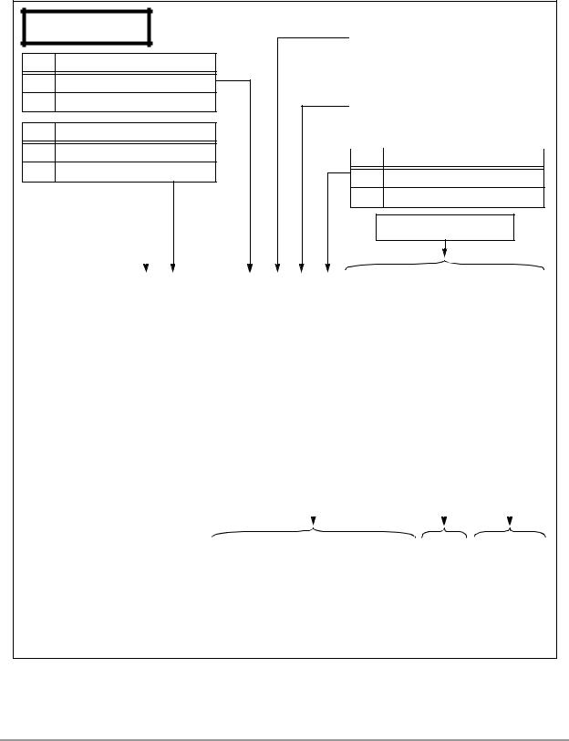
Application: |
|
|
Date: |
|
|
|
|
|
Programmer: |
|
|
Sheet 1 of 1
COP/RTI
RTE |
Description |
0RTE and COP disabled
1RTE and COP enabled
CT |
Description |
0COP timer 8
1COP timer 64
CPE |
Description |
|
|
|
|
|
|
|
0 |
COP disabled |
|
|
|
|
1 |
COP enabled |
|
|
|
|
|
|
|
RTIE |
Description |
|
|
|
|
0 |
Real-time interrupt disabled |
|
|
1 |
Real-time interrupt disabled |
|
|
|
|
RTIF |
Description |
|
|
|
|
0 |
RTE and COP disabled |
|
|
1 |
RTE and COP enabled |
|
|
|
|
RP |
Description |
0Real-time prescaler disabled
1Real-time prescaler enabled, 4
COP/RTI Divider
|
15 |
14 |
13 |
12 |
|
11 |
|
10 |
9 |
8 |
|
7 |
|
6 |
5 |
|
4 |
|
|
3 |
|
2 |
1 |
0 |
|||
|
|
|
|
||||||||||||||||||||||||
COP/RTI Control |
CPE |
CT |
* |
* |
|
RTE |
|
RTIE |
RTIF |
RP |
|
DV7 |
DV6 |
DV5 |
DV4 |
|
|
DV3 |
|
DV2 |
DV1 |
DV0 |
|||||
Register (COPCTL) |
|
|
0 |
0 |
|
|
|
|
|
|
|
|
|
|
|
|
|
|
|
|
|
|
|
|
|
|
|
X:$FFF1 |
|
|
|
|
|
|
|
|
|
|
|
|
|
|
|
|
|
|
|
|
|
|
|
|
|
|
|
|
|
|
|
|
|
|
|
|
|
|
|
|
|
|
|
|
|
|
|
|
|
|
|
|
|
|
|
Reset = $0000 |
|
|
|
|
|
|
|
|
|
|
|
|
|
|
|
|
|
|
|
|
|
|
|
|
|
|
|
|
|
|
|
|
|
|
|
|
|
|
|
|
|
|
|
|
|
|
|
|
|
|
|
|
|
|
|
|
* = Reserved, program as zero |
|
|
|
|
|
|
|
|
|
|
|
|
|
|
|
|
|
|
|
|||||||
|
|
|
|
|
|
|
|
|
|
|
|
|
|
|
|
|
|
|
|
|
|
|
|||||
|
|
|
|
|
|
|
|
|
|
|
|
|
|
|
|
|
|
|
|
Initialized as 111 |
|
||||||
|
|
|
|
|
|
|
|
|
|
|
|
|
|
|
|
|
|
|
|
|
|
|
|
|
|
|
|
|
|
|
|
|
|
|
|
|
|
|
|
|
|
|
|
|
|
|
|
|
|||||||
|
|
|
|
|
|
|
|
|
|
|
|
|
|
|
|
Value Set by RP Bit |
|
|
|
|
|||||||
|
|
|
|
|
|
|
|
|
|
|
|
|
|
|
|
|
|
|
|
|
|
|
|
|
|
|
|
|
|
|
|
|
|
|
|
|
|
|
|
|
|
|
|
|
|
|
|
|
|
|
|||||
|
|
|
|
|
|
|
|
|
COP/RTI Divider |
|
|
|
|
|
|
|
|
|
|
|
|
|
|||||
|
|
|
|
|
|
|
|
|
|
|
|
|
|
|
|
|
|
|
|
|
|
|
|
|
|
|
|
|
|
|
|
|
|
|
|
|
|
|
|
|
|
|
|
|
|
|
|
|
|
|
|
|
|
|
|
COP/RTI Count |
15 |
14 |
13 |
12 |
|
11 |
|
10 |
9 |
8 |
|
7 |
|
6 |
5 |
|
4 |
|
|
3 |
|
2 |
1 |
0 |
|||
|
|
|
|
|
|||||||||||||||||||||||
* |
* |
* |
DV7 |
|
DV6 |
|
DV5 |
DV4 |
DV3 |
|
DV2 |
DV1 |
DV0 |
RP1 |
|
|
RP0 |
|
SC2 |
SC1 |
SC0 |
||||||
|
|
|
|
|
|
|
|
|
|
|
|
|
|
|
|
||||||||||||
Register (COPCNT) |
0 |
0 |
0 |
|
|
|
|
|
|
|
|
|
|
|
|
|
|
|
|
|
|
|
|
|
|
|
|
X:$FFF0 |
|
|
|
|
|
|
|
|
|
|
|
|
|
|
|
|
|
|
|
|
|
|
|
|
|
|
|
|
|
|
|
|
|
|
|
|
|
|
|
|
|
|
|
|
|
|
|
|
|
|
|
|
|
|
|
Reset = $5555 |
|
|
|
|
|
|
|
|
|
|
|
|
|
|
|
|
|
|
|
|
|
|
|
|
|
|
|
|
|
|
|
|
|
|
|
|
|
|
|
|
|
|
|
|
|
|
|
|
|
|
|
||||
|
* = Reserved, program as zero |
|
|
|
|
|
|
|
|
|
|
|
|
|
|
|
|
|
|
|
|||||||
Programmer’s Sheets |
C-33 |

C-34 |
DSP56824 User’s Manual |
|