

- •List of Figures
- •List of Tables
- •List of Examples
- •About This Book
- •1.1 DSP56824 Architecture Overview
- •1.1.1 DSP56824 Peripheral Blocks
- •1.1.1.1 On-Chip Memory
- •1.1.1.2 External Memory Interface (Port A)
- •1.1.1.3 General-Purpose Input/Output Port (Port B)
- •1.1.1.4 Programmable I/O Port (Port C)
- •1.1.1.5 Serial Peripheral Interface (SPI)
- •1.1.1.6 Synchronous Serial Interface (SSI)
- •1.1.1.7 General-Purpose Timer Module
- •1.1.1.8 On-Chip Clock Synthesis Block
- •1.1.1.9 COP/RTI Module
- •1.1.1.10 JTAG/OnCE™ Port
- •1.1.2 DSP56824 Peripheral Interrupts
- •1.2 DSP56800 Core Description
- •1.2.1 Data Arithmetic Logic Unit (Data ALU)
- •1.2.2 Address Generation Unit (AGU)
- •1.2.3 Program Controller and Hardware Looping Unit
- •1.2.4 Bit-Manipulation Unit
- •1.2.5 Address and Data Buses
- •1.2.6 On-Chip Emulation (OnCE) Module
- •1.3 DSP56800 Programming Model
- •1.4 Code Development on the DSP56824
- •2.1 Power and Ground Signals
- •2.2 Clock and Phase Lock Loop (PLL) Signals
- •2.3 External Memory Interface (Port A)
- •2.4 Interrupt and Mode Control Signals
- •2.5 GPIO Signals
- •2.6 Serial Peripheral Interface (SPI) Signals
- •2.7 Synchronous Serial Interface (SSI) Signals
- •2.8 Timer Module Signals
- •2.9 JTAG/OnCE Port Signals
- •3.1 DSP56824 Memory Map
- •3.1.1 X Data Memory
- •3.1.2 Operating Mode Register (OMR)
- •3.1.2.1 Nested Looping (NL)—Bit 15
- •3.1.2.2 Reserved Bits—Bits 14–9
- •3.1.2.3 Condition Codes (CC)—Bit 8
- •3.1.2.4 Reserved Bit—Bit 7
- •3.1.2.5 Stop Delay (SD)—Bit 6
- •3.1.2.6 Rounding (R)—Bit 5
- •3.1.2.7 Saturation (SA)—Bit 4
- •3.1.2.8 External X Memory (EX)—Bit 3
- •3.1.2.9 Reserved Bit—Bit 2
- •3.1.3 DSP56824 Status Register (SR)
- •3.1.4 On-Chip Peripheral Memory Map
- •3.1.5 Program Memory Map
- •3.2 DSP56824 Operating Modes
- •3.2.1 Single Chip Bootstrap Mode (Mode 0)
- •3.2.2 Single Chip User (Mode 1)
- •3.2.3 Normal Expanded Mode (Mode 2)
- •3.2.4 Development Mode (Mode 3)
- •3.3 DSP56824 Reset and Interrupt Vectors
- •3.3.1 DSP56824 Interrupt Priority Register (IPR)
- •3.3.2 Interrupt Priority Structure
- •4.1 External Memory Port Architecture
- •4.2 Port A Description
- •4.2.1 Bus Control Register (BCR)
- •4.2.1.1 Reserved Bits—Bits 15–10
- •4.2.1.2 Drive (DRV)—Bit 9
- •4.2.1.3 Reserved Bit—Bit 8
- •4.2.2 Pins in Different Processing States
- •5.1 Port B Programming Model
- •5.1.1 Port B Data Direction Register (PBDDR)
- •5.1.2 Port B Data (PBD) Register
- •5.1.2.1 PBD Bit Values for General-Purpose Inputs
- •5.1.2.2 PBD Bit Values for General-Purpose Outputs
- •5.1.2.3 PBD Bit Values for Interrupt Inputs
- •5.1.3 Port B Interrupt (PBINT) Register
- •5.2 Port B Interrupt Generation
- •5.3 Port B Programming Examples
- •5.3.1 Receiving Data on Port B
- •5.3.2 Sending Data on Port B
- •5.3.3 Looping Data on Port B
- •5.3.4 Generating Interrupts on Port B
- •6.1 Port C Programming Model
- •6.1.1 Port C Control (PCC) Register
- •6.1.2 Port C Data Direction Register (PCDDR)
- •6.1.3 Port C Data (PCD) Register
- •6.2 Port C Programming Examples
- •6.2.1 Receiving Data on Port C GPIO Pins
- •6.2.2 Sending Data on Port C GPIO Pins
- •6.2.3 Looping Data on Port C GPIO Pins
- •7.1 SPI Architecture
- •7.2 SPI Programming Model
- •7.2.1 SPI Control Registers (SPCR0 and SPCR1)
- •7.2.1.1 Reserved Bits—Bits 15–9
- •7.2.1.2 SPI Clock Rate Select (SPR[2:0])—Bits 8, 1–0
- •7.2.1.3 SPI Interrupt Enable (SPIE)—Bit 7
- •7.2.1.4 SPI Enable (SPE)—Bit 6
- •7.2.1.5 Wired-OR Mode (WOM)—Bit 5
- •7.2.1.6 Master Mode Select (MST)—Bit 4
- •7.2.1.7 Clock Polarity (CPL)—Bit 3
- •7.2.1.8 Clock Phase (CPH)—Bit 2
- •7.2.2 SPI Status Register (SPSR0 and SPSR1)
- •7.2.2.1 Reserved Bits—Bits 15–8
- •7.2.2.2 SPI Interrupt Complete Flag (SPIF)—Bit 7
- •7.2.2.3 Write Collision (WCOL)—Bit 6
- •7.2.2.4 Reserved Bit—Bit 5
- •7.2.2.5 Mode Fault (MDF)—Bit 4
- •7.2.2.6 Reserved Bits—Bits 3–0
- •7.2.3 SPI Data Registers (SPDR0 and SPDR1)
- •7.3 SPI Data and Control Pins
- •7.4 SPI System Errors
- •7.4.1 SPI Mode-Fault Error
- •7.4.2 SPI Write-Collision Error
- •7.4.3 SPI Overrun
- •7.5 Configuring Port C for SPI Functionality
- •7.6 Programming Examples
- •7.6.1 Configuring an SPI Port as Master
- •7.6.2 Configuring an SPI Port as Slave
- •7.6.3 Sending Data from Master to Slave
- •8.1 SSI Architecture
- •8.1.1 SSI Clocking
- •8.1.2 SSI Clock and Frame Sync Generation
- •8.2 SSI Programming Model
- •8.2.1 SSI Transmit Shift Register (TXSR)
- •8.2.2 SSI Transmit Data Buffer Register
- •8.2.3 SSI Transmit Data (STX) Register
- •8.2.4 SSI Receive Shift Register (RXSR)
- •8.2.5 SSI Receive Data Buffer Register
- •8.2.6 SSI Receive Data (SRX) Register
- •8.2.7 SSI Transmit and Receive Control Registers
- •8.2.7.1 Prescaler Range (PSR)—Bit 15
- •8.2.7.2 Word Length Control (WL[1:0])—Bits 14–13
- •8.2.7.3 Frame Rate Divider Control (DC[4:0])—Bits 12–8
- •8.2.7.4 Prescale Modulus Select (PM[7:0])—Bits 7–0
- •8.2.8 SSI Control Register 2 (SCR2)
- •8.2.8.1 Receive Interrupt Enable (RIE)—Bit 15
- •8.2.8.2 Transmit Interrupt Enable (TIE)—Bit 14
- •8.2.8.3 Receive Enable (RE)—Bit 13
- •8.2.8.4 Transmit Enable (TE)—Bit 12
- •8.2.8.5 Receive Buffer Enable (RBF)—Bit 11
- •8.2.8.6 Transmit Buffer Enable (TBF)—Bit 10
- •8.2.8.7 Receive Direction (RXD)—Bit 9
- •8.2.8.8 Transmit Direction (TXD)—Bit 8
- •8.2.8.9 Synchronous Mode (SYN)—Bit 7
- •8.2.8.10 Transmit Shift Direction (TSHFD)—Bit 6
- •8.2.8.11 Transmit Clock Polarity (TSCKP)—Bit 5
- •8.2.8.12 SSI Enable (SSIEN)—Bit 4
- •8.2.8.13 Network Mode (NET)—Bit 3
- •8.2.8.14 Frame Sync Invert (FSI)—Bit 2
- •8.2.8.15 Frame Sync Length (FSL)—Bit 1
- •8.2.8.16 Early Frame Sync (EFS)—Bit 0
- •8.2.9 SSI Control/Status Register (SCSR)
- •8.2.9.1 Reserved Bit—Bit 15
- •8.2.9.2 Receive Shift Direction (RSHFD)—Bit 14
- •8.2.9.3 Receive Clock Polarity (RSCKP)—Bit 13
- •8.2.9.4 Reserved Bits—Bits 12–11
- •8.2.9.5 Receive Frame Sync Invert (RFSI)—Bit 10
- •8.2.9.6 Receive Frame Sync Length (RFSL)—Bit 9
- •8.2.9.7 Receive Early Frame Sync (REFS)—Bit 8
- •8.2.9.8 Receive Data Register Full (RDF)—Bit 7
- •8.2.9.9 Transmit Data Register Empty (TDE)—Bit 6
- •8.2.9.10 Receiver Overrun Error (ROE)—Bit 5
- •8.2.9.11 Transmitter Underrun Error (TUE)—Bit 4
- •8.2.9.12 Transmit Frame Sync (TFS)—Bit 3
- •8.2.9.13 Receive Frame Sync (RFS)—Bit 2
- •8.2.9.14 Receive Data Buffer Full (RDBF)—Bit 1
- •8.2.9.15 Transmit Data Buffer Empty (TDBE)—Bit 0
- •8.2.10 SSI Time Slot Register (STSR)
- •8.3 SSI Data and Control Pins
- •8.4 SSI Operating Modes
- •8.4.1 Normal Mode
- •8.4.1.1 Normal Mode Transmit
- •8.4.1.2 Normal Mode Receive
- •8.4.2 Network Mode
- •8.4.2.1 Network Mode Transmit
- •8.4.2.2 Network Mode Receive
- •8.4.3 Gated Clock Operation
- •8.5 SSI Reset and Initialization Procedure
- •8.6 Configuring Port C for SSI Functionality
- •9.1 Timer Programming Model
- •9.1.1 Timer Control Registers (TCR01 and TCR2)
- •9.1.1.1 Timer Enable (TE)—Bit 15, Bit 7
- •9.1.1.2 Invert (INV)—Bit 6
- •9.1.1.3 Overflow Interrupt Enable (OIE)—Bit 12, Bit 4
- •9.1.1.4 Timer Output Enable (TO[1:0])—Bits 11–10, Bits 3–2
- •9.1.1.5 Event Select (ES[1:0])—Bits 9–8, Bits 1–0
- •9.1.1.6 Reserved TCR Bits
- •9.1.2 Timer Preload Register (TPR)
- •9.1.3 Timer Count Register (TCT)
- •9.2 Timer Resolution
- •9.3 Timer Interrupt Priorities
- •9.4 Event Counting with the Timer Module
- •9.5 Timer Module Low-Power Operation
- •9.5.1 Turning Off the Entire Timer Module
- •9.5.2 Turning Off Any Timer Not in Use
- •9.5.3 Lowering the Timer Frequency
- •9.5.4 Running the Timer in Wait Mode
- •9.5.5 Running the Timer in Stop Mode
- •9.6 Timer Module Timing Diagrams
- •9.7 Configuring Port C for Timer Functionality
- •10.1 Timing System Architecture
- •10.1.1 Oscillator
- •10.1.2 Phase Lock Loop (PLL)
- •10.1.3 Prescaler
- •10.1.4 Clockout Multiplexer (MUX)
- •10.1.5 Control Registers
- •10.2 Clock Synthesis Programming Model
- •10.2.1 PLL Control Register 1 (PCR1)
- •10.2.1.1 Reserved Bit—Bit 15
- •10.2.1.2 PLL Enable (PLLE)—Bit 14
- •10.2.1.3 PLL Power Down (PLLD)—Bit 13
- •10.2.1.4 Low Power Stop (LPST)—Bit 12
- •10.2.1.5 Test Enable (TSTEN)—Bit 11
- •10.2.1.6 Prescaler Divider (PS[2:0])—Bits 10–8
- •10.2.1.7 CLKO Select (CS[1:0])—Bits 7–6
- •10.2.1.8 Reserved Bits—Bits 5–4
- •10.2.1.9 VCO Curve Select (VCS0)—Bit 3
- •10.2.1.10 Reserved Bits—Bits 2–0
- •10.2.2 PLL Control Register 0 (PCR0)
- •10.2.2.1 Reserved Bit—Bit 15
- •10.2.2.2 Feedback Divider (YD[9:0])—Bits 14–5
- •10.2.2.3 Reserved Bits—Bits 4–0
- •10.3 Low-Power Wait and Stop Modes
- •10.3.2 COP, Realtime Clock and CLKO Pin Enabled
- •10.3.3 PLL and CLKO Pin Enabled
- •10.3.4 CLKO Pin Enabled
- •10.3.5 Everything Disabled
- •10.4 PLL Lock
- •10.4.1 PLL Programming Example
- •10.4.2 Changing the PLL Frequency
- •10.4.3 Turning Off the PLL Before Entering Stop Mode
- •10.5 PLL Module Low-Power Operation
- •10.5.1 Turning Off the Entire Clock Synthesis Module
- •10.5.2 Turning Off the Prescaler Divider When Not in Use
- •10.5.3 Turning Off the PLL When Not in Use
- •10.5.4 Turning Off the CLKO Pin When Not in Use
- •11.1 COP and Real-Time Timer Architecture
- •11.2 COP and RTI Timer Programming Model
- •11.2.1 COP and RTI Control Register (COPCTL)
- •11.2.1.1 COP Enable (CPE)—Bit 15
- •11.2.1.2 COP Timer Divider (CT)—Bit 14
- •11.2.1.3 Reserved Bits—Bits 13–12
- •11.2.1.4 RTI Timer Enable (RTE)—Bit 11
- •11.2.1.5 RTI Enable (RTIE)—Bit 10
- •11.2.1.6 RTI Flag (RTIF)—Bit 9
- •11.2.1.7 RTI Prescaler (RP)—Bit 8
- •11.2.1.8 RTI/COP Divider (DV[7:0])—Bits 7–0
- •11.2.2 COP and RTI Count (COPCNT) Register
- •11.2.2.1 Reserved Bits—Bits 15–13
- •11.2.2.2 RTI/COP Divider (DV[7:0])—Bits 12–5
- •11.2.2.3 RTI Prescaler (RP[1:0])—Bits 4–3
- •11.2.2.4 Scaler (SC[2:0])—Bits 2–0
- •11.2.3 COP Reset (COPRST) Register
- •11.3 Programming the COP and RTI Timers
- •11.3.1 COP and RTI Timer Resolution
- •11.3.2 COP/RTI Timer Low-Power Operation
- •11.3.3 Programming Example
- •12.1 Combined JTAG/OnCE Interface Overview
- •12.2 JTAG/OnCE Port Pinout
- •12.3 OnCE Module Architecture
- •12.3.1 OnCE Port Block Diagram
- •12.3.2 OnCE Programming Model
- •12.3.3 OnCE State Machine and Control Block
- •12.4 Command, Status, and Control Registers
- •12.4.1 OnCE Shift Register (OSHR)
- •12.4.2 OnCE Command Register (OCMDR)
- •12.4.3 OnCE Decoder (ODEC)
- •12.4.4 OnCE Control Register (OCR)
- •12.4.4.1 COP Timer Disable (COPDIS)—Bit 15
- •12.4.4.2 DE Pin Output Enable (DE)—Bit 14
- •12.4.4.3 Breakpoint Configuration (BK[4:0])—Bits 13–9
- •12.4.4.4 Debug Request Mask (DRM)—Bit 8
- •12.4.4.5 FIFO Halt (FH)—Bit 7
- •12.4.4.6 Event Modifier (EM[1:0])—Bits 6–5
- •12.4.4.7 Power Down Mode (PWD)—Bit 4
- •12.4.4.8 Breakpoint Selection (BS[1:0])—Bits 3–2
- •12.4.4.9 Breakpoint Enable (BE[1:0])—Bits 1–0
- •12.4.5 OnCE Breakpoint 2 Control Register (OBCTL2)
- •12.4.5.1 Reserved OBCTL2 Register Bits
- •12.4.5.2 Enable (EN)—Bit 2
- •12.4.5.3 Invert (INV)—Bit 1
- •12.4.5.4 Data/Address Select (DAT)—Bit 0
- •12.4.6 OnCE Status Register (OSR)
- •12.4.6.1 Reserved OSR Bits—Bits 7–5
- •12.4.6.2 OnCE Core Status (OS[1:0])—Bits 4–3
- •12.4.6.3 Trace Occurrence (TO)—Bit 2
- •12.4.6.4 Hardware Breakpoint Occurrence (HBO)—Bit 1
- •12.4.6.5 Software Breakpoint Occurrence (SBO)—Bit 0
- •12.5 Breakpoint and Trace Registers
- •12.5.1 OnCE Breakpoint/Trace Counter Register (OCNTR)
- •12.5.2 OnCE Memory Address Latch (OMAL) Register
- •12.5.3 OnCE Breakpoint Address Register (OBAR)
- •12.5.4 OnCE Memory Address Comparator (OMAC)
- •12.5.5 OnCE Breakpoint and Trace Section
- •12.6 Pipeline Registers
- •12.6.1 OnCE PAB Fetch Register (OPABFR)
- •12.6.2 OnCE PAB Decode Register (OPABDR)
- •12.6.3 OnCE PAB Execute Register (OPABER)
- •12.6.4 OnCE PAB Change-of-Flow FIFO (OPFIFO)
- •12.6.5 OnCE PDB Register (OPDBR)
- •12.6.6 OnCE PGDB Register (OPGDBR)
- •12.6.7 OnCE FIFO History Buffer
- •12.7 Breakpoint 2 Architecture
- •12.8 Breakpoint Configuration
- •12.8.1 Programming the Breakpoints
- •12.8.2 OnCE Trace Logic Operation
- •12.9 The Debug Processing State
- •12.9.1 OnCE Normal, Debug, and Stop Modes
- •12.9.2 Entering Debug Mode
- •12.9.2.1 JTAG DEBUG_REQUEST and the Debug Event Pin
- •12.9.2.2 Software Request During Normal Activity
- •12.9.2.3 Trigger Events (Breakpoints and Trace Modes)
- •12.9.2.5 Exiting Debug Mode
- •12.10 Accessing the OnCE Module
- •12.10.1 Primitive JTAG Sequences
- •12.10.2 Entering the JTAG Test-Logic-Reset State
- •12.10.3 Loading the JTAG Instruction Register
- •12.10.4 Accessing a JTAG Data Register
- •12.10.4.1 JTAG/OnCE Interaction: Basic Sequences
- •12.10.4.2 Executing a OnCE Command by Reading the OCR
- •12.10.4.3 Executing a OnCE Command by Writing the OCNTR
- •12.10.4.4 OSR Status Polling
- •12.10.4.5 JTAG IR Status Polling
- •12.10.4.6 TRST/DE Pin Polling
- •12.10.5 Serial Protocol Description
- •12.10.5.1 Entering Debug Mode from User Mode
- •12.10.5.2 Entering Debug Mode from DSP Reset
- •12.10.5.3 Polling for OnCE Status
- •12.10.5.4 Setting Breakpoints in User Mode
- •12.10.5.5 Reading Pipeline Information in User Mode
- •12.10.5.6 Displaying a Specified Register
- •12.10.5.7 Displaying X Memory Area Starting at Address xxxx
- •12.10.5.8 Returning from Debug Mode to Normal Mode
- •12.10.5.9 Recovering from STOP or WAIT Execution
- •12.11 Using the OnCE Port
- •12.11.1 Beginning Debug Activity
- •12.11.2 Displaying a Specified Register
- •12.11.3 Displaying X Memory Area Starting at Address xxxx
- •12.11.4 Returning from Debug Mode to Normal Mode
- •12.12 OnCE Unit Low-Power Operation
- •13.1 JTAG/OnCE Port Pinout
- •13.2 JTAG Port Architecture
- •13.2.1 JTAG Instruction Register (IR) and Decoder
- •13.2.2 JTAG Chip Identification (CID) Register
- •13.2.3 JTAG Boundary Scan Register (BSR)
- •13.2.4 JTAG Bypass Register
- •13.3 TAP Controller
- •13.4 DSP56824 Restrictions
- •A.1 Design Considerations
- •A.1.1 Boot Source Selection
- •A.1.1.1 Bootstrapping from SPI0
- •A.1.1.2 Bootstrapping from Port A
- •A.1.2 COP Reset
- •A.1.3 No Load Option
- •A.2 Bootstrap Listing
- •B.1 DSP56824 BSDL Listing—100-Pin TQFP
- •C.1 Instruction Set Summary
- •C.2 Interrupt, Vector, and Address Tables
- •C.3 Programmer’s Sheets
- •Index

OnCE™ Module
12.9.2.5 Exiting Debug Mode
There are three ways to exit debug mode:
•Restore the pipeline by writing the original OPDBR value back to OPDBR twice, first with
GO = EX = 0 and last with GO = EX = 1. PAB is restored from OPABFR so that fetching continues from the correct address.
•Change program flow by writing a jmp opcode to OPDBR with GO = EX = 0 and then writing the target address to OPDBR with GO = 1 and EX = 0. Next, write a NOP to OPDBR with
GO = EX = 1.
•Apply a hardware reset (assert RESET), which brings the chip out of debug mode provided DEBUG_REQUEST is not decoded in the JTAG IR.
12.10 Accessing the OnCE Module
This section describes useful example sequences involving the JTAG/OnCE interface. The sequences are described in a hierarchical manner. Low-level sequences describe basic operations (for example, JTAG instruction and data register accesses). Building on this, the second group of sequences describe more complicated sequences (for example, OnCE command entry and status polling). The final set builds further on the lower-level sequences to describe how to display core registers, set breakpoints, and change memory.
12.10.1 Primitive JTAG Sequences
The JTAG/OnCE serial protocol is identical to the protocol described in the IEEE Standard Test Access Port and Boundary-Scan Architecture (1149.1a-1993). It involves the control of four input pins—TRST (actually bidirectional), TDI, TMS, and TCK—and the observance of one output pin, TDO. TDI and TDO are the serial input and output, respectively. TCK is the serial clock and TMS is an input used to selectively step through the JTAG state machine. TRST is an asynchronous reset of the JTAG port. It is multiplexed with the DE output function.
The following descriptions refer to states in the JTAG state machine diagram in Figure 13-5 on page 13-13. Please refer to this diagram or to the IEEE 1149.1a-1993 document.
12.10.2 Entering the JTAG Test-Logic-Reset State
The test-logic-reset state is the convenient starting point for primitive JTAG/OnCE module sequences. While in this state, JTAG is reset. This means that TDO is disabled, no shifting is taking place, and the JTAG IR is decoding the IDCODE instruction. This state is entered only on power up or during the initial phase of a series of OnCE module sequences. In addition, this state can be entered to get JTAG into a known state. To enter the test-logic-reset state on power up, both TRST and RESET should be asserted, as shown in Figure 12-15. See the DSP56824 Technical Data Sheet for minimum assertion pulse widths. TRST can change at any time with respect to TCK.
12-40 |
DSP56824 User’s Manual |
|
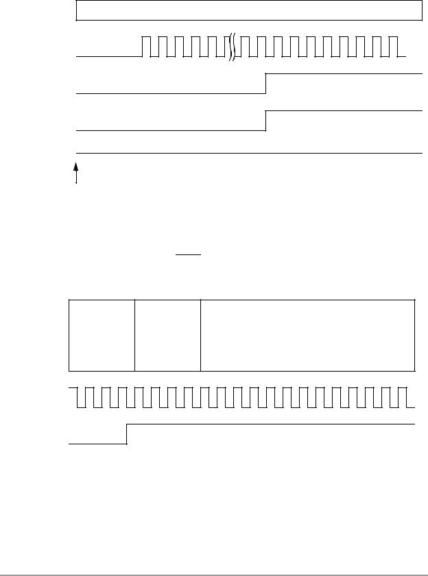
Accessing the OnCE Module
JTAG
Test-Logic-Reset
State
TCK
TRST
RESET
TMS
Power Up |
AA0840 |
Figure 12-15. Entering the JTAG Test-Logic-Reset State
At any other time, the test-logic-reset state can be entered by holding TMS high for five or more TCK pulses, as shown in Figure 12-16. TMS is sampled by the chip on the rising edge of TCK. To explicitly show this timing, TMS is shown to change on the falling edge of TCK. The JTAG state machine changes state on the rising edges of TCK (or on TRST assertion and power up). This sequence provides a simple way of resetting JTAG into a known state.
JTAG
Shift-DR
State
TCK
TMS
Exit1-DR |
Update-DR |
Select-DR-Scan |
Select-IR-Scan |
|
|
|
|
Test-Logic-Reset
AA0841
Figure 12-16. Holding TMS High to Enter Test-Logic-Reset State
|
OnCE™ Module |
12-41 |