

|
|
|
|
|
|
|
|
|
|
|
|
|
|
|
Timer Timing |
||
3.12 |
Timer Timing |
|
|
|
|
|
|
|
|
||||||||
(VSS = 0 V, VDD = 2.7–3.6 V, TA = –40° to +85° C, CL = 50 pF) |
|
|
|
|
|
|
|
|
|||||||||
|
|
|
|
Table 30. Timer Timing |
|
|
|
|
|
|
|
|
|||||
|
|
|
|
|
|
|
|
|
|
|
|
|
|
|
|
|
|
|
|
|
|
|
|
|
|
|
|
|
|
70 MHz |
|
|
|
||
No. |
|
|
|
Characteristic |
|
|
|
|
|
|
|
Unit |
|||||
|
|
|
|
|
|
|
|
|
|
|
Min |
|
Max |
|
|
|
|
|
|
|
|
|
|
|
|
|
|
|
|
|
|
|
|
|
|
|
|
|
|
|
|
|
|
|
|
|
|
|
|
|
|
|
|
150 |
|
Timer input valid to CLKO high (setup time) |
11.4 |
|
— |
|
|
ns |
|||||||||
|
|
|
|
|
|
|
|
|
|
|
|
|
|
|
|
|
|
151 |
|
CLKO high to timer input not valid (hold time) |
0 |
|
— |
|
|
ns |
|||||||||
|
|
|
|
|
|
|
|
|
|
|
|
|
|
|
|
|
|
152 |
|
CLKO high to timer output asserted |
9.5 |
|
18.7 |
|
|
ns |
|||||||||
|
|
|
|
|
|
|
|
|
|
|
|
|
|
|
|
|
|
153 |
|
CLKO high to timer output deasserted |
5.1 |
|
20.7 |
|
|
ns |
|||||||||
|
|
|
|
|
|
|
|
|
|
|
|
|
|
|
|
|
|
154 |
|
Timer input period |
|
8T |
|
— |
|
|
ns |
||||||||
|
|
|
|
|
|
|
|
|
|
|
|
|
|
|
|
|
|
155 |
|
Timer input high/low period |
|
4T |
|
— |
|
|
ns |
||||||||
|
|
|
|
|
|
|
|
|
|
|
|
|
|
|
|
|
|
|
|
|
|
|
|
|
|
|
|
|
|
|
|
|
|
|
|
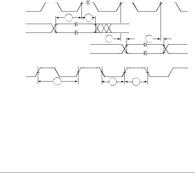
CLKO |
|
|
(Output) |
|
|
150 |
151 |
|
TIO01 |
|
|
TIO2 |
|
|
(Input) |
|
|
|
152 |
153 |
TIO01 |
|
|
TIO2 |
|
|
(Output) |
|
|
TIO01 |
|
|
|
TIO2 |
|
|
|
(Input) |
154 |
155 |
155 |
AA0205
Figure 32. Timer Timing
DSP56824 Technical Data |
47 |
3.13 JTAG Timing
(VSS = 0 V, VDD = 2.7–3.6 V, TA = –40° to +85° C, CL = 50 pF)
Table 31. JTAG Timing
|
|
|
|
|
|
70 MHz |
|
|
No. |
|
|
|
Characteristics |
|
|
|
Unit |
|
|
|
|
|
Min |
|
Max |
|
|
|
|
|
|
|
|
||
|
|
|
|
|
|
|
||
160 |
|
TCK frequency of operation |
|
|
|
|
||
|
|
In OnCE Debug mode (EXTAL/8) |
0.0 |
|
8.75 |
MHz |
||
|
|
In JTAG mode |
0.0 |
|
10 |
MHz |
||
|
|
|
|
|
|
|
||
161 |
|
TCK cycle time |
100 |
|
— |
ns |
||
|
|
|
|
|
|
|
||
162 |
|
TCK clock pulse width |
50 |
|
— |
ns |
||
|
|
|
|
|
|
|
||
164 |
|
Boundary scan input data setup time |
34.5 |
|
— |
ns |
||
|
|
|
|
|
|
|||
165 |
Boundary scan input data hold time |
0 |
|
— |
ns |
|||
|
|
|
|
|
|
|||
166 |
TCK low to output data valid |
— |
|
40.6 |
ns |
|||
|
|
|
|
|
|
|||
167 |
TCK low to output tri-state |
— |
|
43.4 |
ns |
|||
|
|
|
|
|
|
|||
168 |
TMS, TDI data setup time |
0.4 |
|
— |
ns |
|||
|
|
|
|
|
|
|||
169 |
TMS, TDI data hold time |
1.2 |
|
— |
ns |
|||
|
|
|
|
|
|
|||
170 |
TCK low to TDO data valid |
— |
|
26.6 |
ns |
|||
|
|
|
|
|
|
|||
171 |
TCK low to TDO tri-state |
— |
|
23.5 |
ns |
|||
|
|
|
|
|
|
|
|
|
172 |
|
|
|
assertion time |
50 |
|
— |
ns |
|
TRST |
|||||||
|
|
|
|
|
|
|
|
|
173 |
|
|
assertion time |
8T |
|
— |
ns |
|
|
DE |
|||||||
|
|
|
|
|
|
|
|
|
Note: Timing is both wait state and frequency dependent. In the formulas listed, WS = the number of wait states and T = 1/2 the clock cycle. For 70 MHz operation, T = 7.14 ns.
|
|
|
|
|
|
|
|
|
|
|
|
|
|
|
161 |
|
|
|
|
|
|
|
|
|
|
|
|
|
|
|
|
|
|
|
|
|||||||||||
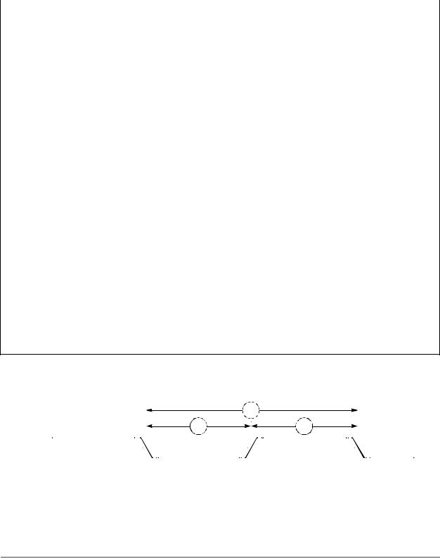
|
VIH |
|
|
|
162 |
|
|
|
|
|
|
|
|
|
|
162 |
|
|
|
|
|
|
|
|
|
|
|
|
||||||||||||||||||
|
|
|
|
|
|
|
|
|
|
|
|
|
|
|
|
|
|
|||||||||||||||||||||||||||||
|
|
|
|
|
|
|
|
|
|
|
|
|
|
|
|
|
|
|
|
|
|
|
|
|
|
|
|
|
|
|
|
|
|
|
|
|
|
|
|
|
|
|
||||
TCK |
|
|
|
|
|
|
|
|
|
VM |
|
|
|
|
|
|
|
|
|
|
|
|
|
|
|
|
|
|
VM |
|
|
|
|
|
||||||||||||
|
|
|
|
|
|
|
|
|
|
|
|
|
|
|
|
|
|
|
|
|
|
|
|
|
|
|
|
|
|
|
|
|
|
|
|
|
|
|
|
|
|
|
|
|||
(Input) |
|
|
|
|
|
|
|
|
|
|
|
|
|
|
|
|
|
|
|
|
|
|
|
|
|
|
|
|
|
|
|
|
|
|
|
|
|
|
|
|
|
|
||||
|
|
|
|
|
|
VIL |
|
|
|
|
|
|
|
|
|
|
|
|
|
|
|
|
|
|
|
|
|
|
|
|
|
|
|
|
|
|
|
|
||||||||
VM = VIL + (VIH – VIL)/2 |
|
|
|
|
|
|
|
|
|
|
|
|
|
|
|
|
|
|
|
|
|
|
|
|
|
|
|
|
|
|
|
|
|
|
|
|
AA1453 |
|||||||||
|
|
|
|
|
|
|
|
|
|
|
|
|
|
|
|
|
|
|
|
|
|
|
|
|
|
|
|
|
|
|
|
|
|
|
|
|
|
|
||||||||
Figure 33. Test Clock Input Timing Diagram
48 |
DSP56824 Technical Data |
|
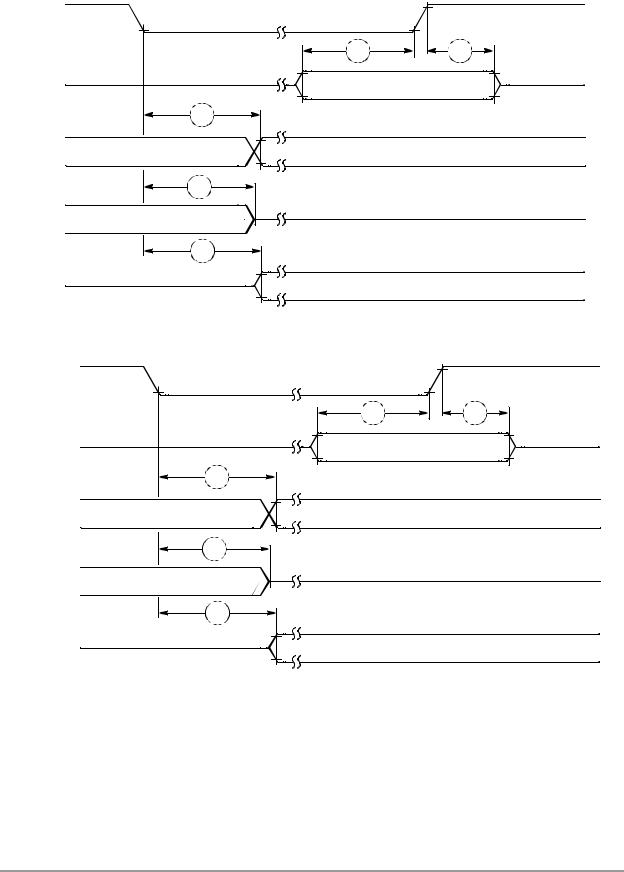
TCK (Input)
Data
Inputs
Data
Outputs
Data
Outputs
Data
Outputs
TCK (Input)
TDI
TMS  (Input)
TDO (Output)
TDO (Output)
TDO (Output)
JTAG Timing
164 |
165 |
Input Data Valid
166
Output Data Valid
167
166
Output Data Valid
AA0207
Figure 34. Boundary Scan (JTAG) Timing Diagram
168 |
169 |
Input Data Valid
170
Output Data Valid
171
170
Output Data Valid
AA0208
Figure 35. Test Access Port Timing Diagram
DSP56824 Technical Data |
49 |
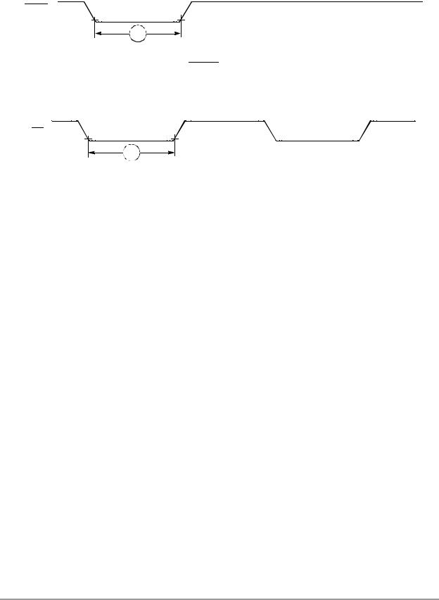
TRST
(Input)
172
AA0209
Figure 36. TRST Timing Diagram
DE
173
AA0210
Figure 37. OnCE—Debug Event
50 |
DSP56824 Technical Data |
|