

- •About This Book
- •1.1 DSP56800 Family Architecture
- •1.1.1 Core Overview
- •1.1.2 Peripheral Blocks
- •1.1.3 Family Members
- •1.2 Introduction to Digital Signal Processing
- •1.3 Summary of Features
- •1.4 For the Latest Information
- •2.1 Core Block Diagram
- •2.1.1 Data Arithmetic Logic Unit (ALU)
- •2.1.2 Address Generation Unit (AGU)
- •2.1.3 Program Controller and Hardware Looping Unit
- •2.1.4 Bus and Bit-Manipulation Unit
- •2.1.5 On-Chip Emulation (OnCE) Unit
- •2.1.6 Address Buses
- •2.1.7 Data Buses
- •2.2 Memory Architecture
- •2.3 Blocks Outside the DSP56800 Core
- •2.3.1 External Data Memory
- •2.3.2 Program Memory
- •2.3.3 Bootstrap Memory
- •2.3.4 IP-BUS Bridge
- •2.3.5 Phase Lock Loop (PLL)
- •2.4 DSP56800 Core Programming Model
- •3.1 Overview and Architecture
- •3.1.1 Data ALU Input Registers (X0, Y1, and Y0)
- •3.1.2 Data ALU Accumulator Registers
- •3.1.3 Multiply-Accumulator (MAC) and Logic Unit
- •3.1.4 Barrel Shifter
- •3.1.5 Accumulator Shifter
- •3.1.6 Data Limiter and MAC Output Limiter
- •3.2 Accessing the Accumulator Registers
- •3.2.1 Accessing an Accumulator by Its Individual Portions
- •3.2.2 Accessing an Entire Accumulator
- •3.2.2.1 Accessing for Data ALU Operations
- •3.2.2.2 Writing an Accumulator with a Small Operand
- •3.2.2.3 Extension Registers as Protection Against Overflow
- •3.2.2.4 Examples of Writing the Entire Accumulator
- •3.2.3 General Integer Processing
- •3.2.3.1 Writing Integer Data to an Accumulator
- •3.2.3.2 Reading Integer Data from an Accumulator
- •3.2.4 Using 16-Bit Results of DSP Algorithms
- •3.2.5 Saving and Restoring Accumulators
- •3.2.6 Bit-Field Operations on Integers in Accumulators
- •3.2.7 Converting from 36-Bit Accumulator to 16-Bit Portion
- •3.3 Fractional and Integer Data ALU Arithmetic
- •3.3.1 Interpreting Data
- •3.3.2 Data Formats
- •3.3.2.1 Signed Fractional
- •3.3.2.2 Unsigned Fractional
- •3.3.2.3 Signed Integer
- •3.3.2.4 Unsigned Integer
- •3.3.3 Addition and Subtraction
- •3.3.4 Logical Operations
- •3.3.5 Multiplication
- •3.3.5.1 Fractional Multiplication
- •3.3.5.2 Integer Multiplication
- •3.3.6 Division
- •3.3.7 Unsigned Arithmetic
- •3.3.7.1 Conditional Branch Instructions for Unsigned Operations
- •3.3.7.2 Unsigned Multiplication
- •3.3.8 Multi-Precision Operations
- •3.3.8.1 Multi-Precision Addition and Subtraction
- •3.3.8.2 Multi-Precision Multiplication
- •3.4 Saturation and Data Limiting
- •3.4.1 Data Limiter
- •3.4.2 MAC Output Limiter
- •3.4.3 Instructions Not Affected by the MAC Output Limiter
- •3.5 Rounding
- •3.5.1 Convergent Rounding
- •3.5.2 Two’s-Complement Rounding
- •3.6 Condition Code Generation
- •3.6.1 36-Bit Destinations—CC Bit Cleared
- •3.6.2 36-Bit Destinations—CC Bit Set
- •3.6.3 20-Bit Destinations—CC Bit Cleared
- •3.6.4 20-Bit Destinations—CC Bit Set
- •3.6.5 16-Bit Destinations
- •3.6.6 Special Instruction Types
- •3.6.7 TST and TSTW Instructions
- •3.6.8 Unsigned Arithmetic
- •4.1 Architecture and Programming Model
- •4.1.1 Address Registers (R0-R3)
- •4.1.2 Stack Pointer Register (SP)
- •4.1.3 Offset Register (N)
- •4.1.4 Modifier Register (M01)
- •4.1.5 Modulo Arithmetic Unit
- •4.1.6 Incrementer/Decrementer Unit
- •4.2 Addressing Modes
- •4.2.1 Register-Direct Modes
- •4.2.1.1 Data or Control Register Direct
- •4.2.1.2 Address Register Direct
- •4.2.2 Address-Register-Indirect Modes
- •4.2.2.1 No Update: (Rn), (SP)
- •4.2.2.2 Post-Increment by 1: (Rn)+, (SP)+
- •4.2.2.3 Post-Decrement by 1: (Rn)-, (SP)-
- •4.2.2.4 Post-Update by Offset N: (Rn)+N, (SP)+N
- •4.2.2.5 Index by Offset N: (Rn+N), (SP+N)
- •4.2.2.6 Index by Short Displacement: (SP-xx), (R2+xx)
- •4.2.2.7 Index by Long Displacement: (Rn+xxxx), (SP+xxxx)
- •4.2.3 Immediate Data Modes
- •4.2.3.1 Immediate Data: #xxxx
- •4.2.3.2 Immediate Short Data: #xx
- •4.2.4 Absolute Addressing Modes
- •4.2.4.1 Absolute Address (Extended Addressing): xxxx
- •4.2.4.2 Absolute Short Address (Direct Addressing): <aa>
- •4.2.4.3 I/O Short Address (Direct Addressing): <pp>
- •4.2.5 Implicit Reference
- •4.2.6 Addressing Modes Summary
- •4.3 AGU Address Arithmetic
- •4.3.1 Linear Arithmetic
- •4.3.2 Modulo Arithmetic
- •4.3.2.1 Modulo Arithmetic Overview
- •4.3.2.2 Configuring Modulo Arithmetic
- •4.3.2.3 Supported Memory Access Instructions
- •4.3.2.4 Simple Circular Buffer Example
- •4.3.2.5 Setting Up a Modulo Buffer
- •4.3.2.6 Wrapping to a Different Bank
- •4.3.2.7 Side Effects of Modulo Arithmetic
- •4.3.2.7.1 When a Pointer Lies Outside a Modulo Buffer
- •4.3.2.7.2 Restrictions on the Offset Register
- •4.3.2.7.3 Memory Locations Not Available for Modulo Buffers
- •4.4 Pipeline Dependencies
- •5.1 Architecture and Programming Model
- •5.1.1 Program Counter
- •5.1.2 Instruction Latch and Instruction Decoder
- •5.1.3 Interrupt Control Unit
- •5.1.4 Looping Control Unit
- •5.1.5 Loop Counter
- •5.1.6 Loop Address
- •5.1.7 Hardware Stack
- •5.1.8 Status Register
- •5.1.8.1 Carry (C)—Bit 0
- •5.1.8.2 Overflow (V)—Bit 1
- •5.1.8.3 Zero (Z)—Bit 2
- •5.1.8.4 Negative (N)—Bit 3
- •5.1.8.5 Unnormalized (U)—Bit 4
- •5.1.8.6 Extension (E)—Bit 5
- •5.1.8.7 Limit (L)—Bit 6
- •5.1.8.8 Size (SZ)—Bit 7
- •5.1.8.9 Interrupt Mask (I1 and I0)—Bits 8–9
- •5.1.8.10 Reserved SR Bits— Bits 10–14
- •5.1.8.11 Loop Flag (LF)—Bit 15
- •5.1.9 Operating Mode Register
- •5.1.9.1 Operating Mode Bits (MB and MA)—Bits 1–0
- •5.1.9.2 External X Memory Bit (EX)—Bit 3
- •5.1.9.3 Saturation (SA)—Bit 4
- •5.1.9.4 Rounding Bit (R)—Bit 5
- •5.1.9.5 Stop Delay Bit (SD)—Bit 6
- •5.1.9.6 Condition Code Bit (CC)—Bit 8
- •5.1.9.7 Nested Looping Bit (NL)—Bit 15
- •5.1.9.8 Reserved OMR Bits—Bits 2, 7 and 9–14
- •5.2 Software Stack Operation
- •5.3 Program Looping
- •5.3.1 Repeat (REP) Looping
- •5.3.2 DO Looping
- •5.3.3 Nested Hardware DO and REP Looping
- •5.3.4 Terminating a DO Loop
- •6.1 Introduction to Moves and Parallel Moves
- •6.2 Instruction Formats
- •6.3 Programming Model
- •6.4 Instruction Groups
- •6.4.1 Arithmetic Instructions
- •6.4.2 Logical Instructions
- •6.4.3 Bit-Manipulation Instructions
- •6.4.4 Looping Instructions
- •6.4.5 Move Instructions
- •6.4.6 Program Control Instructions
- •6.5 Instruction Aliases
- •6.5.1 ANDC, EORC, ORC, and NOTC Aliases
- •6.5.2 LSLL Alias
- •6.5.3 ASL Alias
- •6.5.4 CLR Alias
- •6.5.5 POP Alias
- •6.6 DSP56800 Instruction Set Summary
- •6.6.1 Register Field Notation
- •6.6.2 Using the Instruction Summary Tables
- •6.6.3 Instruction Summary Tables
- •6.7 The Instruction Pipeline
- •6.7.1 Instruction Processing
- •6.7.2 Memory Access Processing
- •7.1 Reset Processing State
- •7.2 Normal Processing State
- •7.2.1 Instruction Pipeline Description
- •7.2.2 Instruction Pipeline with Off-Chip Memory Accesses
- •7.2.3 Instruction Pipeline Dependencies and Interlocks
- •7.3 Exception Processing State
- •7.3.1 Sequence of Events in the Exception Processing State
- •7.3.2 Reset and Interrupt Vector Table
- •7.3.3 Interrupt Priority Structure
- •7.3.4 Configuring Interrupt Sources
- •7.3.5 Interrupt Sources
- •7.3.5.1 External Hardware Interrupt Sources
- •7.3.5.2 DSP Core Hardware Interrupt Sources
- •7.3.5.3 DSP Core Software Interrupt Sources
- •7.3.6 Interrupt Arbitration
- •7.3.7 The Interrupt Pipeline
- •7.3.8 Interrupt Latency
- •7.4 Wait Processing State
- •7.5 Stop Processing State
- •7.6 Debug Processing State
- •8.1 Useful Instruction Operations
- •8.1.1 Jumps and Branches
- •8.1.1.1 JRSET and JRCLR Operations
- •8.1.1.2 BR1SET and BR1CLR Operations
- •8.1.1.3 JR1SET and JR1CLR Operations
- •8.1.1.4 JVS, JVC, BVS, and BVC Operations
- •8.1.1.5 Other Jumps and Branches on Condition Codes
- •8.1.2 Negation Operations
- •8.1.2.1 NEGW Operation
- •8.1.2.2 Negating the X0, Y0, or Y1 Data ALU registers
- •8.1.2.3 Negating an AGU register
- •8.1.2.4 Negating a Memory Location
- •8.1.3 Register Exchanges
- •8.1.4 Minimum and Maximum Values
- •8.1.4.1 MAX Operation
- •8.1.4.2 MIN Operation
- •8.1.5 Accumulator Sign Extend
- •8.1.6 Unsigned Load of an Accumulator
- •8.2.2 General 16-Bit Shifts
- •8.2.3 General 32-Bit Arithmetic Right Shifts
- •8.2.5 Arithmetic Shifts by a Fixed Amount
- •8.2.5.1 Right Shifts (ASR12–ASR20)
- •8.2.5.2 Left Shifts (ASL16–ASL19)
- •8.3 Incrementing and Decrementing Operations
- •8.4 Division
- •8.4.1 Positive Dividend and Divisor with Remainder
- •8.4.2 Signed Dividend and Divisor with No Remainder
- •8.4.3 Signed Dividend and Divisor with Remainder
- •8.4.4 Algorithm Examples
- •8.4.5 Overflow Cases
- •8.5 Multiple Value Pushes
- •8.6 Loops
- •8.6.1 Large Loops (Count Greater Than 63)
- •8.6.2 Variable Count Loops
- •8.6.3 Software Loops
- •8.6.4 Nested Loops
- •8.6.4.1 Recommendations
- •8.6.4.2 Nested Hardware DO and REP Loops
- •8.6.4.3 Comparison of Outer Looping Techniques
- •8.6.5 Hardware DO Looping in Interrupt Service Routines
- •8.6.6 Early Termination of a DO Loop
- •8.7 Array Indexes
- •8.7.1 Global or Fixed Array with a Constant
- •8.7.2 Global or Fixed Array with a Variable
- •8.7.3 Local Array with a Constant
- •8.7.4 Local Array with a Variable
- •8.7.5 Array with an Incrementing Pointer
- •8.8 Parameters and Local Variables
- •8.9 Time-Critical DO Loops
- •8.10 Interrupts
- •8.10.1 Setting Interrupt Priorities in Software
- •8.10.1.1 High Priority or a Small Number of Instructions
- •8.10.1.2 Many Instructions of Equal Priority
- •8.10.1.3 Many Instructions and Programmable Priorities
- •8.10.2 Hardware Looping in Interrupt Routines
- •8.10.3 Identifying System Calls by a Number
- •8.11 Jumps and JSRs Using a Register Value
- •8.12 Freeing One Hardware Stack Location
- •8.13 Multitasking and the Hardware Stack
- •8.13.1 Saving the Hardware Stack
- •8.13.2 Restoring the Hardware Stack
- •9.1 Combined JTAG and OnCE Interface
- •9.2 JTAG Port
- •9.2.1 JTAG Capabilities
- •9.2.2 JTAG Port Architecture
- •9.3 OnCE Port
- •9.3.1 OnCE Port Capabilities
- •9.3.2 OnCE Port Architecture
- •9.3.2.1 Command, Status, and Control
- •9.3.2.2 Breakpoint and Trace
- •9.3.2.3 Pipeline Save and Restore
- •9.3.2.4 FIFO History Buffer
- •A.1 Notation
- •A.2 Programming Model
- •A.3 Addressing Modes
- •A.4 Condition Code Computation
- •A.4.1 The Condition Code Bits
- •A.4.1.1 Size (SZ)—Bit 7
- •A.4.1.2 Limit (L)—Bit 6
- •A.4.1.3 Extension in Use (E)—Bit 5
- •A.4.1.4 Unnormalized (U)—Bit 4
- •A.4.1.5 Negative (N)—Bit 3
- •A.4.1.6 Zero (Z)—Bit 2
- •A.4.1.7 Overflow (V)—Bit 1
- •A.4.1.8 Carry (C)—Bit 0
- •A.4.2 Effects of the Operating Mode Register’s SA Bit
- •A.4.3 Effects of the OMR’s CC Bit
- •A.4.4 Condition Code Summary by Instruction
- •A.5 Instruction Timing
- •A.6 Instruction Set Restrictions
- •A.7 Instruction Descriptions
- •B.1 Benchmark Code
- •B.1.1 Real Correlation or Convolution (FIR Filter)
- •B.1.2 N Complex Multiplies
- •B.1.3 Complex Correlation Or Convolution (Complex FIR)
- •B.1.4 Nth Order Power Series (Real, Fractional Data)
- •B.1.5 N Cascaded Real Biquad IIR Filters (Direct Form II)
- •B.1.6 N Radix 2 FFT Butterflies
- •B.1.7 LMS Adaptive Filter
- •B.1.7.1 Single Precision
- •B.1.7.2 Double Precision
- •B.1.7.3 Double Precision Delayed
- •B.1.8 Vector Multiply-Accumulate
- •B.1.9 Energy in a Signal
- •B.1.10 [3x3][1x3] Matrix Multiply
- •B.1.11 [NxN][NxN] Matrix Multiply
- •B.1.12 N Point 3x3 2-D FIR Convolution
- •B.1.13 Sine-Wave Generation
- •B.1.13.1 Double Integration Technique
- •B.1.13.2 Second Order Oscillator
- •B.1.14 Array Search
- •B.1.14.1 Index of the Highest Signed Value
- •B.1.14.2 Index of the Highest Positive Value
- •B.1.15 Proportional Integrator Differentiator (PID) Algorithm
JTAG and On-Chip Emulation (OnCE™ ) |
|
|
|
JTAG |
OnCE |
|
|
OnCE Command, |
|
Test |
Status & Control |
|
|
|
External |
Access |
XAB1 |
Interface |
Port |
PAB |
|
||
|
Controller |
Breakpoint Logic |
|
|
|
|
|
Trace Logic |
|
|
Event Counter |
|
|
PDB |
|
|
PGDB |
|
|
Pipeline |
|
|
Registers |
|
|
PAB |
|
|
FIFO |
|
|
History |
|
|
Buffer |
|
|
AA0093 |
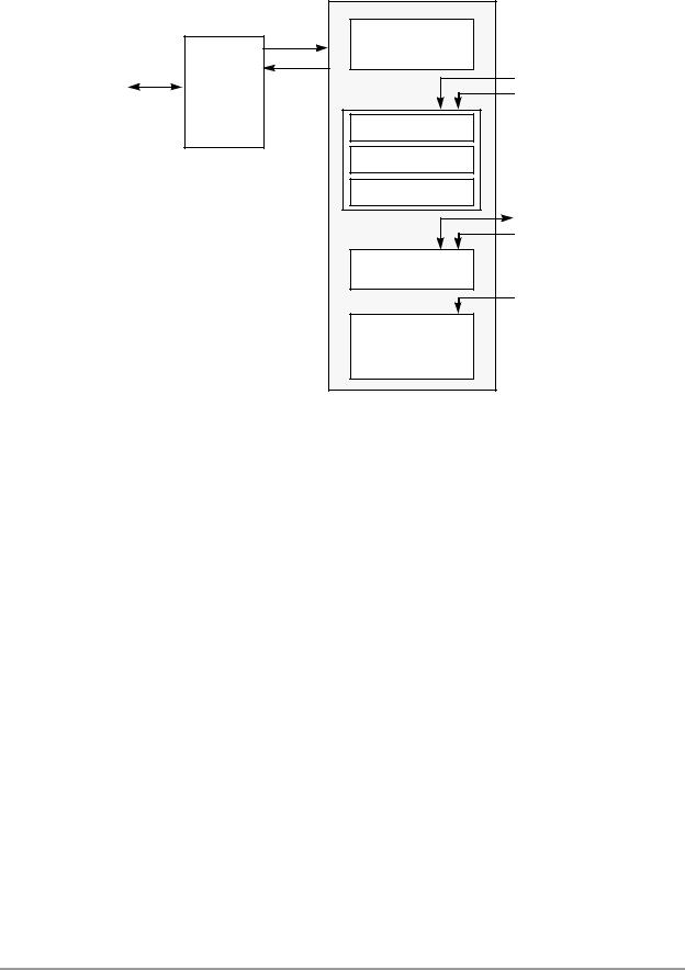
Figure 9-1. JTAG/OnCE Interface Block Diagram
As already noted, the JTAG module is the master. It enables interaction with the debug services provided by the OnCE, and its external serial interface is used by the OnCE port for sending and receiving debugging commands and data.
9.2 JTAG Port
Problems associated with testing high-density circuit boards have led to the development of a proposed standard under the sponsorship of the Test Technology Committee of IEEE and the Joint Test Action Group (JTAG). The resulting standard, called the IEEE Standard Test Access Port and Boundary-Scan Architecture, specifies industry-standard, in-circuit device testing and diagnosis. The DSP56800 family provides a dedicated test access port (TAP) that is fully compatible with this standard, commonly referred to as the “JTAG port.”
This section provides an overview of the capabilities of the JTAG port as implemented on the DSP56800. Information provided here is intended to supplement the supporting IEEE 1149.1a-1993 document, which outlines the internal details, applications, and overall methodology of the standard. Specific details on the implementation of the JTAG port for a given DSP56800-based device are provided in that device’s user’s manual.
9-2 |
DSP56800 Family Manual |
|

JTAG Port
9.2.1 JTAG Capabilities
The DSP56800 JTAG port has the following capabilities:
•Performing boundary scan operations to test circuit-board electrical continuity
•Sampling the DSP56800-based device system pins during operation and transparently shifting out the result in the boundary scan register; preloading values to output pins prior to performing a boundary scan operation
•Querying identification information (manufacturer, part number, and version) from a DSP56800-based device
•Adding a weak pull-up device on all input signals to cause all open inputs to report a logic 1 and to force a predictable internal state while performing external boundary scan operations
•Disabling the output drive to pins during circuit-board testing
•Forcing test data onto the outputs of a DSP56800-based device
•Providing a means of accessing the OnCE controller and circuits to control a target system
•Providing a means of entering the debug mode of operation
•Bypassing the DSP56800 core for a given circuit-board test by effectively reducing the boundary scan register to a single cell
Section 9.2.2, “JTAG Port Architecture,” provides an overview of the port’s architecture and commands. For additional information on the JTAG port’s implementation and command set, see the appropriate DSP56800-based device’s user’s manual.
9.2.2 JTAG Port Architecture
The JTAG module consists of the logic necessary to support boundary scan testing as defined in the IEEE specification. Although tightly coupled to the DSP56800’s core logic, it is an independent module, and, when disabled, it is guaranteed to have no impact on the function of the core.
The JTAG port consists of the following components:
•Serial communications interface
•Command decoder and interpreter
•Boundary scan register
•ID register
These units, and the overall once port architecture, are shown in Figure 9-2 on page 9-4.
JTAG and On-Chip Emulation (OnCE™ ) |
9-3 |