
- •About This Book
- •1.1 DSP56800 Family Architecture
- •1.1.1 Core Overview
- •1.1.2 Peripheral Blocks
- •1.1.3 Family Members
- •1.2 Introduction to Digital Signal Processing
- •1.3 Summary of Features
- •1.4 For the Latest Information
- •2.1 Core Block Diagram
- •2.1.1 Data Arithmetic Logic Unit (ALU)
- •2.1.2 Address Generation Unit (AGU)
- •2.1.3 Program Controller and Hardware Looping Unit
- •2.1.4 Bus and Bit-Manipulation Unit
- •2.1.5 On-Chip Emulation (OnCE) Unit
- •2.1.6 Address Buses
- •2.1.7 Data Buses
- •2.2 Memory Architecture
- •2.3 Blocks Outside the DSP56800 Core
- •2.3.1 External Data Memory
- •2.3.2 Program Memory
- •2.3.3 Bootstrap Memory
- •2.3.4 IP-BUS Bridge
- •2.3.5 Phase Lock Loop (PLL)
- •2.4 DSP56800 Core Programming Model
- •3.1 Overview and Architecture
- •3.1.1 Data ALU Input Registers (X0, Y1, and Y0)
- •3.1.2 Data ALU Accumulator Registers
- •3.1.3 Multiply-Accumulator (MAC) and Logic Unit
- •3.1.4 Barrel Shifter
- •3.1.5 Accumulator Shifter
- •3.1.6 Data Limiter and MAC Output Limiter
- •3.2 Accessing the Accumulator Registers
- •3.2.1 Accessing an Accumulator by Its Individual Portions
- •3.2.2 Accessing an Entire Accumulator
- •3.2.2.1 Accessing for Data ALU Operations
- •3.2.2.2 Writing an Accumulator with a Small Operand
- •3.2.2.3 Extension Registers as Protection Against Overflow
- •3.2.2.4 Examples of Writing the Entire Accumulator
- •3.2.3 General Integer Processing
- •3.2.3.1 Writing Integer Data to an Accumulator
- •3.2.3.2 Reading Integer Data from an Accumulator
- •3.2.4 Using 16-Bit Results of DSP Algorithms
- •3.2.5 Saving and Restoring Accumulators
- •3.2.6 Bit-Field Operations on Integers in Accumulators
- •3.2.7 Converting from 36-Bit Accumulator to 16-Bit Portion
- •3.3 Fractional and Integer Data ALU Arithmetic
- •3.3.1 Interpreting Data
- •3.3.2 Data Formats
- •3.3.2.1 Signed Fractional
- •3.3.2.2 Unsigned Fractional
- •3.3.2.3 Signed Integer
- •3.3.2.4 Unsigned Integer
- •3.3.3 Addition and Subtraction
- •3.3.4 Logical Operations
- •3.3.5 Multiplication
- •3.3.5.1 Fractional Multiplication
- •3.3.5.2 Integer Multiplication
- •3.3.6 Division
- •3.3.7 Unsigned Arithmetic
- •3.3.7.1 Conditional Branch Instructions for Unsigned Operations
- •3.3.7.2 Unsigned Multiplication
- •3.3.8 Multi-Precision Operations
- •3.3.8.1 Multi-Precision Addition and Subtraction
- •3.3.8.2 Multi-Precision Multiplication
- •3.4 Saturation and Data Limiting
- •3.4.1 Data Limiter
- •3.4.2 MAC Output Limiter
- •3.4.3 Instructions Not Affected by the MAC Output Limiter
- •3.5 Rounding
- •3.5.1 Convergent Rounding
- •3.5.2 Two’s-Complement Rounding
- •3.6 Condition Code Generation
- •3.6.1 36-Bit Destinations—CC Bit Cleared
- •3.6.2 36-Bit Destinations—CC Bit Set
- •3.6.3 20-Bit Destinations—CC Bit Cleared
- •3.6.4 20-Bit Destinations—CC Bit Set
- •3.6.5 16-Bit Destinations
- •3.6.6 Special Instruction Types
- •3.6.7 TST and TSTW Instructions
- •3.6.8 Unsigned Arithmetic
- •4.1 Architecture and Programming Model
- •4.1.1 Address Registers (R0-R3)
- •4.1.2 Stack Pointer Register (SP)
- •4.1.3 Offset Register (N)
- •4.1.4 Modifier Register (M01)
- •4.1.5 Modulo Arithmetic Unit
- •4.1.6 Incrementer/Decrementer Unit
- •4.2 Addressing Modes
- •4.2.1 Register-Direct Modes
- •4.2.1.1 Data or Control Register Direct
- •4.2.1.2 Address Register Direct
- •4.2.2 Address-Register-Indirect Modes
- •4.2.2.1 No Update: (Rn), (SP)
- •4.2.2.2 Post-Increment by 1: (Rn)+, (SP)+
- •4.2.2.3 Post-Decrement by 1: (Rn)-, (SP)-
- •4.2.2.4 Post-Update by Offset N: (Rn)+N, (SP)+N
- •4.2.2.5 Index by Offset N: (Rn+N), (SP+N)
- •4.2.2.6 Index by Short Displacement: (SP-xx), (R2+xx)
- •4.2.2.7 Index by Long Displacement: (Rn+xxxx), (SP+xxxx)
- •4.2.3 Immediate Data Modes
- •4.2.3.1 Immediate Data: #xxxx
- •4.2.3.2 Immediate Short Data: #xx
- •4.2.4 Absolute Addressing Modes
- •4.2.4.1 Absolute Address (Extended Addressing): xxxx
- •4.2.4.2 Absolute Short Address (Direct Addressing): <aa>
- •4.2.4.3 I/O Short Address (Direct Addressing): <pp>
- •4.2.5 Implicit Reference
- •4.2.6 Addressing Modes Summary
- •4.3 AGU Address Arithmetic
- •4.3.1 Linear Arithmetic
- •4.3.2 Modulo Arithmetic
- •4.3.2.1 Modulo Arithmetic Overview
- •4.3.2.2 Configuring Modulo Arithmetic
- •4.3.2.3 Supported Memory Access Instructions
- •4.3.2.4 Simple Circular Buffer Example
- •4.3.2.5 Setting Up a Modulo Buffer
- •4.3.2.6 Wrapping to a Different Bank
- •4.3.2.7 Side Effects of Modulo Arithmetic
- •4.3.2.7.1 When a Pointer Lies Outside a Modulo Buffer
- •4.3.2.7.2 Restrictions on the Offset Register
- •4.3.2.7.3 Memory Locations Not Available for Modulo Buffers
- •4.4 Pipeline Dependencies
- •5.1 Architecture and Programming Model
- •5.1.1 Program Counter
- •5.1.2 Instruction Latch and Instruction Decoder
- •5.1.3 Interrupt Control Unit
- •5.1.4 Looping Control Unit
- •5.1.5 Loop Counter
- •5.1.6 Loop Address
- •5.1.7 Hardware Stack
- •5.1.8 Status Register
- •5.1.8.1 Carry (C)—Bit 0
- •5.1.8.2 Overflow (V)—Bit 1
- •5.1.8.3 Zero (Z)—Bit 2
- •5.1.8.4 Negative (N)—Bit 3
- •5.1.8.5 Unnormalized (U)—Bit 4
- •5.1.8.6 Extension (E)—Bit 5
- •5.1.8.7 Limit (L)—Bit 6
- •5.1.8.8 Size (SZ)—Bit 7
- •5.1.8.9 Interrupt Mask (I1 and I0)—Bits 8–9
- •5.1.8.10 Reserved SR Bits— Bits 10–14
- •5.1.8.11 Loop Flag (LF)—Bit 15
- •5.1.9 Operating Mode Register
- •5.1.9.1 Operating Mode Bits (MB and MA)—Bits 1–0
- •5.1.9.2 External X Memory Bit (EX)—Bit 3
- •5.1.9.3 Saturation (SA)—Bit 4
- •5.1.9.4 Rounding Bit (R)—Bit 5
- •5.1.9.5 Stop Delay Bit (SD)—Bit 6
- •5.1.9.6 Condition Code Bit (CC)—Bit 8
- •5.1.9.7 Nested Looping Bit (NL)—Bit 15
- •5.1.9.8 Reserved OMR Bits—Bits 2, 7 and 9–14
- •5.2 Software Stack Operation
- •5.3 Program Looping
- •5.3.1 Repeat (REP) Looping
- •5.3.2 DO Looping
- •5.3.3 Nested Hardware DO and REP Looping
- •5.3.4 Terminating a DO Loop
- •6.1 Introduction to Moves and Parallel Moves
- •6.2 Instruction Formats
- •6.3 Programming Model
- •6.4 Instruction Groups
- •6.4.1 Arithmetic Instructions
- •6.4.2 Logical Instructions
- •6.4.3 Bit-Manipulation Instructions
- •6.4.4 Looping Instructions
- •6.4.5 Move Instructions
- •6.4.6 Program Control Instructions
- •6.5 Instruction Aliases
- •6.5.1 ANDC, EORC, ORC, and NOTC Aliases
- •6.5.2 LSLL Alias
- •6.5.3 ASL Alias
- •6.5.4 CLR Alias
- •6.5.5 POP Alias
- •6.6 DSP56800 Instruction Set Summary
- •6.6.1 Register Field Notation
- •6.6.2 Using the Instruction Summary Tables
- •6.6.3 Instruction Summary Tables
- •6.7 The Instruction Pipeline
- •6.7.1 Instruction Processing
- •6.7.2 Memory Access Processing
- •7.1 Reset Processing State
- •7.2 Normal Processing State
- •7.2.1 Instruction Pipeline Description
- •7.2.2 Instruction Pipeline with Off-Chip Memory Accesses
- •7.2.3 Instruction Pipeline Dependencies and Interlocks
- •7.3 Exception Processing State
- •7.3.1 Sequence of Events in the Exception Processing State
- •7.3.2 Reset and Interrupt Vector Table
- •7.3.3 Interrupt Priority Structure
- •7.3.4 Configuring Interrupt Sources
- •7.3.5 Interrupt Sources
- •7.3.5.1 External Hardware Interrupt Sources
- •7.3.5.2 DSP Core Hardware Interrupt Sources
- •7.3.5.3 DSP Core Software Interrupt Sources
- •7.3.6 Interrupt Arbitration
- •7.3.7 The Interrupt Pipeline
- •7.3.8 Interrupt Latency
- •7.4 Wait Processing State
- •7.5 Stop Processing State
- •7.6 Debug Processing State
- •8.1 Useful Instruction Operations
- •8.1.1 Jumps and Branches
- •8.1.1.1 JRSET and JRCLR Operations
- •8.1.1.2 BR1SET and BR1CLR Operations
- •8.1.1.3 JR1SET and JR1CLR Operations
- •8.1.1.4 JVS, JVC, BVS, and BVC Operations
- •8.1.1.5 Other Jumps and Branches on Condition Codes
- •8.1.2 Negation Operations
- •8.1.2.1 NEGW Operation
- •8.1.2.2 Negating the X0, Y0, or Y1 Data ALU registers
- •8.1.2.3 Negating an AGU register
- •8.1.2.4 Negating a Memory Location
- •8.1.3 Register Exchanges
- •8.1.4 Minimum and Maximum Values
- •8.1.4.1 MAX Operation
- •8.1.4.2 MIN Operation
- •8.1.5 Accumulator Sign Extend
- •8.1.6 Unsigned Load of an Accumulator
- •8.2.2 General 16-Bit Shifts
- •8.2.3 General 32-Bit Arithmetic Right Shifts
- •8.2.5 Arithmetic Shifts by a Fixed Amount
- •8.2.5.1 Right Shifts (ASR12–ASR20)
- •8.2.5.2 Left Shifts (ASL16–ASL19)
- •8.3 Incrementing and Decrementing Operations
- •8.4 Division
- •8.4.1 Positive Dividend and Divisor with Remainder
- •8.4.2 Signed Dividend and Divisor with No Remainder
- •8.4.3 Signed Dividend and Divisor with Remainder
- •8.4.4 Algorithm Examples
- •8.4.5 Overflow Cases
- •8.5 Multiple Value Pushes
- •8.6 Loops
- •8.6.1 Large Loops (Count Greater Than 63)
- •8.6.2 Variable Count Loops
- •8.6.3 Software Loops
- •8.6.4 Nested Loops
- •8.6.4.1 Recommendations
- •8.6.4.2 Nested Hardware DO and REP Loops
- •8.6.4.3 Comparison of Outer Looping Techniques
- •8.6.5 Hardware DO Looping in Interrupt Service Routines
- •8.6.6 Early Termination of a DO Loop
- •8.7 Array Indexes
- •8.7.1 Global or Fixed Array with a Constant
- •8.7.2 Global or Fixed Array with a Variable
- •8.7.3 Local Array with a Constant
- •8.7.4 Local Array with a Variable
- •8.7.5 Array with an Incrementing Pointer
- •8.8 Parameters and Local Variables
- •8.9 Time-Critical DO Loops
- •8.10 Interrupts
- •8.10.1 Setting Interrupt Priorities in Software
- •8.10.1.1 High Priority or a Small Number of Instructions
- •8.10.1.2 Many Instructions of Equal Priority
- •8.10.1.3 Many Instructions and Programmable Priorities
- •8.10.2 Hardware Looping in Interrupt Routines
- •8.10.3 Identifying System Calls by a Number
- •8.11 Jumps and JSRs Using a Register Value
- •8.12 Freeing One Hardware Stack Location
- •8.13 Multitasking and the Hardware Stack
- •8.13.1 Saving the Hardware Stack
- •8.13.2 Restoring the Hardware Stack
- •9.1 Combined JTAG and OnCE Interface
- •9.2 JTAG Port
- •9.2.1 JTAG Capabilities
- •9.2.2 JTAG Port Architecture
- •9.3 OnCE Port
- •9.3.1 OnCE Port Capabilities
- •9.3.2 OnCE Port Architecture
- •9.3.2.1 Command, Status, and Control
- •9.3.2.2 Breakpoint and Trace
- •9.3.2.3 Pipeline Save and Restore
- •9.3.2.4 FIFO History Buffer
- •A.1 Notation
- •A.2 Programming Model
- •A.3 Addressing Modes
- •A.4 Condition Code Computation
- •A.4.1 The Condition Code Bits
- •A.4.1.1 Size (SZ)—Bit 7
- •A.4.1.2 Limit (L)—Bit 6
- •A.4.1.3 Extension in Use (E)—Bit 5
- •A.4.1.4 Unnormalized (U)—Bit 4
- •A.4.1.5 Negative (N)—Bit 3
- •A.4.1.6 Zero (Z)—Bit 2
- •A.4.1.7 Overflow (V)—Bit 1
- •A.4.1.8 Carry (C)—Bit 0
- •A.4.2 Effects of the Operating Mode Register’s SA Bit
- •A.4.3 Effects of the OMR’s CC Bit
- •A.4.4 Condition Code Summary by Instruction
- •A.5 Instruction Timing
- •A.6 Instruction Set Restrictions
- •A.7 Instruction Descriptions
- •B.1 Benchmark Code
- •B.1.1 Real Correlation or Convolution (FIR Filter)
- •B.1.2 N Complex Multiplies
- •B.1.3 Complex Correlation Or Convolution (Complex FIR)
- •B.1.4 Nth Order Power Series (Real, Fractional Data)
- •B.1.5 N Cascaded Real Biquad IIR Filters (Direct Form II)
- •B.1.6 N Radix 2 FFT Butterflies
- •B.1.7 LMS Adaptive Filter
- •B.1.7.1 Single Precision
- •B.1.7.2 Double Precision
- •B.1.7.3 Double Precision Delayed
- •B.1.8 Vector Multiply-Accumulate
- •B.1.9 Energy in a Signal
- •B.1.10 [3x3][1x3] Matrix Multiply
- •B.1.11 [NxN][NxN] Matrix Multiply
- •B.1.12 N Point 3x3 2-D FIR Convolution
- •B.1.13 Sine-Wave Generation
- •B.1.13.1 Double Integration Technique
- •B.1.13.2 Second Order Oscillator
- •B.1.14 Array Search
- •B.1.14.1 Index of the Highest Signed Value
- •B.1.14.2 Index of the Highest Positive Value
- •B.1.15 Proportional Integrator Differentiator (PID) Algorithm

Address Generation Unit
This chapter covers the architecture and programming model of the address generation unit, its addressing modes, and a discussion of the linear and modulo arithmetic capabilities of this unit. It concludes with a discussion of pipeline dependencies related to the address generation unit.
4.1 Architecture and Programming Model
The major components of the address generation unit are as follows:
•Four address registers (R0-R3)
•A stack pointer register (SP)
•An offset register (N)
•A modifier register (M01)
•A modulo arithmetic unit
•An incrementer/decrementer unit
The AGU uses integer arithmetic to perform the effective address calculations necessary to address data operands in memory. The AGU also contains the registers used to generate the addresses. It implements linear and modulo arithmetic and operates in parallel with other chip resources to minimize address-generation overhead.
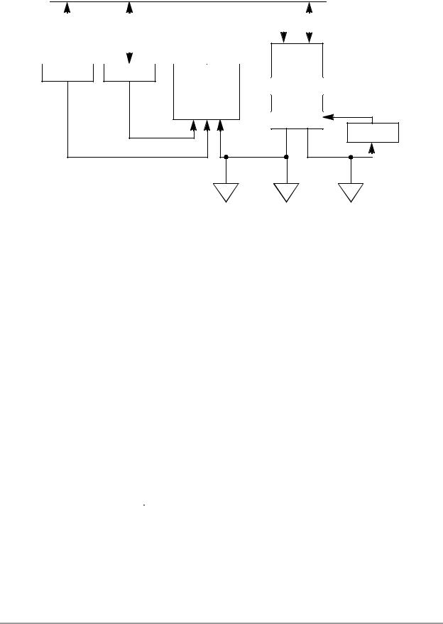
Two ALUs are present within the AGU: the modulo arithmetic unit and the incrementer/decrementer unit. The two arithmetic units can generate up to two 16-bit addresses and two address updates every instruction cycle: one for XAB1 and one for XAB2 for instructions performing two parallel memory reads. The AGU can directly address 65,536 locations on XAB1 and 65,536 locations on the PAB. The AGU can directly address up to 65,536 locations on XAB2, but can only generate addresses to on-chip memory. The two ALUs work with the data memory to access up to two locations and provide two operands to the data ALU in a single cycle. The primary operand is addressed with the XAB1, and the second operand is addressed with the XAB2. The data memory, in turn, places its data on the core global data bus (CGDB) and the second external data bus (XDB2), respectively (see Figure 4-1 on page 4-3). See Section 6.1, “Introduction to Moves and Parallel Moves,” on page 6-1 for more discussion on parallel memory moves.
4-2 |
DSP56800 Family Manual |
|

Architecture and Programming Model
CGDB(15:0)
|
|
|
|
|
|
|
|
|
|
|
|
|
|
|
|
|
|
|
|
|
|
|
|
|
|
|
|
|
|
|
|
|
|
|
|
|
|
|
|
|
|
|
|
|
|
SP |
|
|
|
|
|
|
|
|
|
|
|||
|
|
|
|
|
|
|
|
|
|
|
|
|
|
|
|
|
|
|
|
|
|
R0 |
|
M01 |
N |
|
Modulo
R1
Arithmetic
Unit R2
R3
Inc./Dec.
R3 Only
|
|
|
|
|
|
|
|
|
|
|
|
|
|
|
|
|
|
|
|
|
|
|
|
|
|
|
|
|
|
|
|
|
|
|
|
PAB(15:0) |
XAB1(15:0) |
XAB2(15:0) |
|||||||||
|
|
|
|
|
|
|
|
|
|
|
AA0014 |
Figure 4-1. Address Generation Unit Block Diagram
All four address pointer registers and the SP are used in generating addresses in the register indirect addressing modes. The offset register can be used by all four address pointer registers and the SP, whereas the modulo register can be used by the R0 or by both the R0 and R1 pointer registers.
Whereas all the address pointer registers and the SP can be used in many addressing modes, there are some instructions that only work with a specific address pointer register. These cases are presented in Table 4-5 on page 4-9.
The address generation unit is connected to four major buses: CGDB, XAB1, XAB2, and PAB. The CGDB is used to read or write any of the address generation unit registers. The XAB1 and XAB2 provide a primary and secondary address, respectively, to the X data memory, and the PAB provides the address when accessing the program memory.
A block diagram of the address generation unit is shown in Figure 4-1, and its corresponding programming model is shown in Figure 4-2. The blocks and registers are explained in the following subsections.
15 |
0 |
|
15 |
0 |
15 |
0 |
|
|
|
R0 |
|
|
N |
|
|
M01 |
|
|
|
|
|
|
|
|
|
|
|
R1 |
|
|
|
|
|
|
|
|
|
|
|
|
|
|
|
|
|
R2 |
|
|
|
|
|
|
|
|
|
|
|
|
|
|
|
|
|
R3 |
|
|
|
|
|
|
|
|
|
|
|
|
|
|
|
|
|
SP |
|
|
|
|
|
|
|
|
|
|
|
|
|
|
|
|
|
Pointer |
|
Offset |
|
|
Modifier |
||
|
Registers |
|
Register |
|
|
Register |
||
|
|
|
|
|
|
|
|
AA0015 |
Figure 4-2. Address Generation Unit Programming Model
|
Address Generation Unit |
4-3 |

Address Generation Unit
4.1.1 Address Registers (R0-R3)
The address register file consists of four 16-bit registers R0-R3 (Rn) that usually contain addresses used as pointers to memory. Each register may be read or written by the CGDB. High speed access to the XAB1, XAB2, and PAB buses is required to allow maximum access time for the internal and external X data memory and program memory. Each address register may be used as input for the modulo arithmetic unit for a register update calculation. Each register may be written by the output of the modulo arithmetic unit.
The R3 register may be used as input to a separate incrementer/decrementer unit for an independent register update calculation. This unit is used in the case of any instruction that performs two data memory reads in its parallel move field. For instructions where two reads are performed from the X data memory, the second read using the R3 pointer must always access on-chip memory.
NOTE:
Due to pipelining, if an address register (Rn, SP, or M01) is changed with a MOVE or bit-field instruction, the new contents will not be available for use as a pointer until the second following instruction. If the SP is changed, no LEA or POP instructions are permitted until the second following instruction.
4.1.2 Stack Pointer Register (SP)
The stack pointer register (SP) is a single 16-bit register that is used implicitly in all PUSH instruction macros and POP instructions. The SP is used explicitly for memory references when used with the address-register-indirect modes. It is post-decremented on all POPs from the software stack. The SP register may be read or written by the CGDB.
NOTE:
This register must be initialized explicitly by the programmer after coming out of reset.
Due to pipelining, if an address register (Rn, SP, or M01) is changed with a MOVE or bit-field instruction, the new contents will not be available for use as a pointer until the second following instruction. If the SP is changed, no LEA or POP instructions are permitted until the second following instruction.
4.1.3 Offset Register (N)
The offset register (N) usually contains offset values used to update address pointers. This single register can be used to update or index with any of the address registers (R0-R3, SP). This offset register may be read or written by the CGDB. The offset register is used as input to the modulo arithmetic unit. It is often used for array indexing or indexing into a table, as discussed in Section 8.7, “Array Indexes,” on page 8-26.
4-4 |
DSP56800 Family Manual |
|

Architecture and Programming Model
NOTE:
If the N address register is changed with a MOVE instruction, this register’s contents will be available for use on the immediately following instruction. In this case the instruction that writes the N address register will be stretched one additional instruction cycle. This is true for the case when the N register is used by the immediately following instruction; if N is not used, then the instruction is not stretched an additional cycle. If the N address register is changed with a bit-field instruction, the new contents will not be available for use until the second following instruction.
4.1.4 Modifier Register (M01)
The modifier register (M01) specifies whether linear or modulo arithmetic is used when calculating a new address and may be read or written by the CGDB. This modifier register is automatically read when the R0 address register is used in an address calculation and can optionally be used also when R1 is used. This register has no effect on address calculations done with the R2, R3, or SP registers. It is used as input to the modulo arithmetic unit. This modifier register is preset during a processor reset to $FFFF (linear arithmetic).
NOTE:
Due to pipelining, if an address register (Rn, SP, or M01) is changed with a MOVE or bit-field instruction, the new contents will not be available for use as a pointer until the second following instruction. If the SP is changed, no LEA or POP instructions are permitted until the following instruction.
4.1.5 Modulo Arithmetic Unit
The modulo arithmetic unit can update one address register or the SP during one instruction cycle. It is capable of performing linear and modulo arithmetic, as described in Section 4.3, “AGU Address Arithmetic.” The contents of the modifier register specifies the type of arithmetic to be performed in an address register update calculation. The modifier value is decoded in the modulo arithmetic unit and affects the unit’s operation. The modulo arithmetic unit’s operation is data-dependent and requires execution cycle decoding of the selected modifier register contents. Note that the modulo capability is only allowed for R0 or R1 updates; it is not allowed for R2, R3, or SP updates.
The modulo arithmetic unit first calculates the result of linear arithmetic (for example, Rn+1, Rn-1, Rn+N) which is selected as the modulo arithmetic unit’s output for linear arithmetic. For modulo arithmetic, the modulo arithmetic unit will perform the function (Rn+N) modulo (M01+1), where N can be 1, -1, or the contents of the offset register N. If the modulo operation requires “wraparound” for modulo arithmetic, the summed output of the modulo adder will give the correct, updated address register value; otherwise, if wraparound is not necessary, the linear arithmetic calculation gives the correct result.
4.1.6 Incrementer/Decrementer Unit
The incrementer/decrementer unit is used for address-update calculations during dual data-memory read instructions. It is used either to increment or decrement the R3 register. This adder performs only linear arithmetic; it performs no modulo arithmetic.
|
Address Generation Unit |
4-5 |