

SECTION 2
SPECIFICATIONS
GENERAL CHARACTERISTICS
The DSP56824 is fabricated in high-density CMOS with Transistor-Transistor Logic (TTL)-compatible inputs, 5-volt tolerant Input/Output (I/O), and CMOS-compatible outputs.
Absolute maximum ratings given in Table 2-1 are stress ratings only, and functional operation at the maximum is not guaranteed. Stress beyond these ratings may affect device reliability or cause permanent damage to the device.
The DSP56824 dc/ac electrical specifications are preliminary and are from design simulations. These specifications may not be fully tested or guaranteed at this early stage of the product life cycle. Finalized specifications will be published after complete characterization and device qualifications have been completed.
CAUTION
This device contains protective circuitry to guard against damage due to high static voltage or electrical fields. However, normal precautions are advised to avoid application of any voltages higher than maximum rated voltages to this high-impedance circuit. Reliability of operation is enhanced if unused inputs are tied to an appropriate logic voltage level (e.g., either or VCC or GND).
PRELIMINARY
MOTOROLA |
DSP56824 Technical Data Sheet |
2-1 |

Specifications
General Characteristics
Table 2-1 Absolute Maximum Ratings (GND = 0 V)
Rating |
Symbol |
Value |
Unit |
|
|
|
|
|
|
|
|
Supply voltage |
VDD |
–0.3 to 4.0 |
V |
All other input voltages |
VIN |
(GND – 0.3) to (VDD + 0.3) |
V |
Current drain per pin excluding VDD and GND |
I |
10 |
mA |
|
|
|
|
Storage temperature range |
TSTG |
–55 to 150 |
˚C |
Table 2-2 Recommended Operating Conditions
Characteristic |
Symbol |
Value |
Unit |
|
|
|
|
|
|
|
|
Supply voltage |
VDD |
2.7 to 3.6 |
V |
Ambient temperature |
TA |
–40 to 85 |
˚C |
|
|
|
|
Table 2-3 Package Thermal Characteristics
Thermal Resistance1 |
|
100-pin TQFP |
|
|
|
|
|
|
|
Symbol |
|
Value |
Unit |
|
|
|
|||
|
|
|
|
|
|
|
|
|
|
Junction-to-ambient (estimated)2 |
|
|
65 |
˚C/W |
Junction-to-case (estimated)3 |
RθJC |
|
10 |
˚C/W |
Notes: 1. See discussion under Design Considerations, page 4-1.
2.Junction-to-ambient thermal resistance is based on measurements on a horizontal single-sided Printed Circuit Board per SEMI G38-87 in natural convection. SEMI is Semiconductor Equipment and Materials International, 805 East Middlefield Road, Mountain View, CA 94043, (415) 964-5111.
3.Junction-to-case thermal resistance is based on measurements using a cold plate per SEMI G30-88 with the exception that the cold plate temperature is used for the case temperature.
PRELIMINARY
2-2 |
DSP56824 Technical Data Sheet |
MOTOROLA |

Specifications
DC Electrical Characteristics
DC ELECTRICAL CHARACTERISTICS
Table 2-4 DC Electrical Characteristics
|
Characteristics |
Symbol |
Min |
Typ |
Max |
Unit |
|
|
|
|
|
|
|
|
|
|
|
|
|
|
Supply voltage |
VDD |
2.7 |
— |
3.6 |
V |
|
Input high voltage: |
|
0.8 × VDD |
|
|
V |
|
• |
EXTAL |
VIHC |
— |
VDD |
|
|
• |
All other inputs |
VIH |
2.0 |
— |
5 |
|
Input low voltage |
|
|
|
0.2 × VDD |
V |
|
• |
EXTAL |
VILC |
–0.3 |
— |
|
|
• |
All other inputs |
VIL |
–0.3 |
— |
0.8 |
|
Input leakage current @ 2.4 V/0.4 V with VDD = 3.6 V |
IIN |
–1 |
— |
1 |
µA |
|
Input/output tri-state (off-state) leakage current |
ITSI |
–10 |
— |
+10 |
µA |
|
@ 2.4 V/0.4 V with VDD = 3.6 V |
|
|
|
|
|
|
Output high voltage |
VOH |
|
|
|
V |
|
• |
IOH = –0.3 mA |
|
VDD – 0.7 |
— |
— |
|
• |
IOH = –50 µA |
|
VDD – 0.3 |
— |
— |
|
Output low voltage |
VOL |
|
|
|
V |
|
• IOL = 2 mA |
|
— |
— |
0.4 |
|
|
• IOL = 50 µA) |
|
— |
— |
0.2 |
|
|
Core CPU supply current1 (FPLL = 70 MHz) |
ICORE |
— |
20 |
30 |
mA |
|
Stop mode current1, 2 |
ISTOP |
— |
2 |
5 |
µA |
|
Input capacitance (estimated) |
CIN |
— |
10 |
— |
pF |
|
Notes: |
1. To obtain these results, all inputs must be terminated (i.e., not allowed to float) using CMOS levels. |
|||||
|
2. At 25˚C, VDD = 3.0 V, VIH = VDD, VIL = 0 V. |
|
|
|
|
|
PRELIMINARY
MOTOROLA |
DSP56824 Technical Data Sheet |
2-3 |

Specifications
AC Electrical Characteristics
AC ELECTRICAL CHARACTERISTICS
(VSS = 0 V, VDD = 2.7–3.6 V, TA = –40° to +85°C, CL = 50 pF)
Timing waveforms in AC Electrical Characteristics are tested with a VIL maximum of 0.8 V and a VIH minimum of 2.0 V for all pins except EXTAL, which is tested using the input levels in DC Electrical Characteristics. Figure 2-1 shows the levels of VIH and VIL for an input signal.
|
|
|
Pulse Width |
|
VIH |
Low |
High |
Input Signal |
|
|
90% |
Midpoint1 |
|
50% |
|
|
|
10% |
|
|
|
VIL |
|
|
Fall Time |
Rise Time |
Note: The midpoint is VIL + (VIH – VIL)/2.
AA1447
Figure 2-1 Input Signal Measurement Reference
Figure 2-2 shows the definitions of the following signal states:
•Active state, when a bus or signal is driven , and enters a low impedance state.
•Tristated, when a bus or signal is placed in a high impedance state.
•Data Valid state, when a signal level has reached VOL orVOH.
•Data Invalid state, when a signal level is in transition between VOL and VOH.
Data1 Valid |
Data2 Valid |
Data3 Valid |
Data1 |
Data2 |
Data3 |
Data Invalid State |
|
Data |
|
Tristated |
|
|
|
|
|
Data Active |
Data Active |
AA1448
Figure 2-2 Signal States
PRELIMINARY
2-4 |
DSP56824 Technical Data Sheet |
MOTOROLA |

Specifications
AC Electrical Characteristics
External Clock Operation
(VSS = 0 V, VDD = 2.7–3.6 V, TA = –40° to +85°C, CL = 50 pF)
The DSP56824 system clock can be derived from a crystal or an external system clock signal. To generate a reference frequency using the internal oscillator, a reference crystal must be connected between the EXTAL and XTAL pins. Figure 2-3 shows the transconductance model for XTAL. Table 2-5 shows the electrical characteristics for EXTAL and XTAL pins.
|
|
|
|
|
Vout |
|
|
V |
in |
× g |
m |
r |
Vin |
V |
out |
|
|
o |
|
|
AA0118
Figure 2-3 XTAL Transconductance Model
Table 2-5 EXTAL/XTAL Electrical Characteristics
|
|
|
Characteristics |
Symbol |
Min |
Typ |
Max |
Unit |
||
|
|
|
|
|
|
|
|
|||
|
|
|
|
|
|
|
|
|||
EXTAL peak-to-peak swing (for any value of |
|
|
|
|
|
|
|
|||
XCOLF) |
|
|
|
|
|
|||||
• VDDPLL = 2.7 V |
— |
1.27 |
— |
1.9 |
V p-p |
|||||
• VDDPLL = 3.0 V |
— |
1.38 |
— |
2.1 |
V p-p |
|||||
• VDDPLL = 3.6 V |
— |
1.58 |
— |
2.75 |
V p-p |
|||||
XTAL transconductance |
gm |
|
|
|
|
|||||
• |
XCOLF |
= 0 |
|
0.206 |
0.465 |
1.02 |
mA/V |
|||
• |
XCOLF |
= VDD |
|
2.06 |
4.65 |
10.2 |
mA/V |
|||
XTAL output resistance |
ro |
|
|
|
kΩ |
|||||
• |
XCOLF |
= 0 |
|
28.3 |
80.6 |
209.4 |
||||
• |
XCOLF |
= VDD |
|
2.83 |
8.06 |
20.94 |
kΩ |
|||
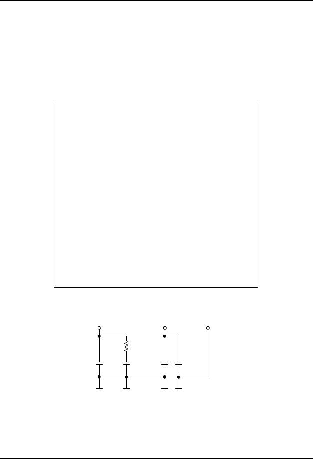
The internal oscillator is designed to interface with a parallel-resonant crystal resonator in the frequency range specified for the external crystal in Table 2-6. Figure 2-4 shows typical crystal oscillator circuits. Follow the crystal supplier’s recommendations when selecting a crystal, since crystal parameters determine the component values required to provide maximum stability and reliable start-up. The load capacitance values used in the oscillator circuit design should include all stray layout capacitances. The crystal and associated components should be mounted as close as possible to the EXTAL and XTAL pins to minimize output distortion and start-up stabilization time.
PRELIMINARY
MOTOROLA |
DSP56824 Technical Data Sheet |
2-5 |

Specifications
AC Electrical Characteristics
When using the on-chip oscillator in conjunction with an external crystal to generate the DSP clock, the following specifications apply. When driving the clock directly into EXTAL (not using a crystal), the input clock should follow normal digital DSP56824 requirements.
Crystal Frequency = 32 kHz or 38.4 kHz
EXTAL XTAL  Rx
Rx 
 Ry
Ry
Cw |
|
|
|
|
|
|
|
Cx |
||||
|
|
|
|
|
|
|||||||
|
|
|
|
|
|
|||||||
|
|
|
|
|
|
|
|
|
|
|
|
|
XCOLF = 0
Rx = 10 MΩ, Ry = 330 kΩ
Cw = 12 pF, Cx = 19 pF
Example Crystal Parameters: Motional capacitance, C1 = 2.3 fF Motional inductance, L1 = 7.47 kH Series resistance, RS = 36 kΩ Shunt capacitance, C0 = 1 pF Load capacitance, CL = 12 pF
(Assumes pin and trace capacitance on the EXTAL and XTAL pins is 9 pF each)
Crystal Frequency = 2–10 MHz
XCOLF = 1
EXTAL |
XTAL |
Rz |
|
Cy |
Cz |
Rz = 10 MΩ
Cy, Cz = 31 pF
Example Crystal Parameters: Series resistance, RS = 36 kΩ Shunt capacitance, C0 = 7 pF Load capacitance, CL = 20 pF (Assumes pin and trace capacitance on the EXTAL and
XTAL pins is 9 pF each)
AA0180
Figure 2-4 Examples of Crystal Oscillator Circuits
If the design uses an external clock circuit, apply the external clock input to the EXTAL input with the XTAL pin left unconnected, as shown in Figure 2-5.
DSP56824 |
|
|
|||
EXTAL |
XTAL |
|
|
||
|
|
|
|
|
|
External |
Not |
|
|||
Clock |
Connected |
AA1449 |
|||
Figure 2-5 Connecting an External Clock Signal
PRELIMINARY
2-6 |
DSP56824 Technical Data Sheet |
MOTOROLA |

Specifications
AC Electrical Characteristics
Table 2-6 Clock Operation Timing
|
|
|
|
|
|
|
|
|
|
|
70 MHz |
|
||
No. |
Characteristics |
|
|
Unit |
||||||||||
Min |
Max |
|||||||||||||
|
|
|
|
|
|
|
|
|
|
|
|
|||
|
|
|
|
|
|
|
||||||||
|
|
|
|
|
|
|
||||||||
1 |
Frequency of operation (external clock) |
0 |
70 |
MHz |
||||||||||
|
|
|
|
|
|
|
||||||||
2 |
Clock cycle time |
14.29 |
— |
ns |
||||||||||
|
|
|
|
|
|
|
||||||||
3 |
Instruction cycle time |
28.57 |
— |
ns |
||||||||||
|
|
|
|
|
|
|
||||||||
4 |
External reference frequency |
|
|
|
||||||||||
|
• Crystal option, |
|
|
|
|
= 01 |
|
|
|
32 |
38.4 |
kHz |
||
|
XCOLF |
|||||||||||||
|
• Crystal option, |
XCOLF |
= 1 |
|
|
|
2 |
10 |
MHz |
|||||
|
• External clock option, |
XCOLF |
= 0 |
0 |
2 |
MHz |
||||||||
|
• External clock option, |
XCOLF |
= 1 |
2 |
70 |
MHz |
||||||||
|
|
|
|
|
|
|
||||||||
5 |
External clock input rise time |
— |
3 |
ns |
||||||||||
|
|
|
|
|
|
|
||||||||
6 |
External clock input fall time |
— |
3 |
ns |
||||||||||
|
|
|
|
|
|
|
||||||||
7 |
External clock input high time |
11.25 |
— |
ns |
||||||||||
|
|
|
|
|
|
|
||||||||
8 |
External clock input low time |
11.25 |
— |
ns |
||||||||||
|
|
|
|
|
|
|
||||||||
9 |
PLL output frequency |
10 |
70 |
MHz |
||||||||||
|
|
|
|
|
|
|
||||||||
10 |
PLL stabilization time after crystal oscillator start-up time2 |
— |
10 |
ms |
||||||||||
|
|
|
|
|
|
|
|
|
|
|
|
|
|
|
Notes: 1. When the crystal option is used and XCOLF = 0, only frequencies of 32 kHz and 38.4 kHz are supported.
2. This is the minimum time required after the PLL setup is changed to ensure reliable operation.
|
|
3 |
VIH |
External |
90% |
|
90% |
Clock |
50% |
|
50% |
|
10% |
|
10% |
|
7 |
8 |
VIL |
|
|
6 |
5 |
|
|
2 |
|
Note: 1. |
The midpoint is VIL + (VIH – VIL)/2. |
AA0182 |
|
|
|
|
|
Figure 2-6 External Clock Timing
PRELIMINARY
MOTOROLA |
DSP56824 Technical Data Sheet |
2-7 |
Specifications
AC Electrical Characteristics
External Components for the PLL
The on-chip PLL requires an extra circuit connected to the SXFC pin, as shown in Figure 2-7. As indicated in Table 2-7, the values of R, C1, and C should be chosen based on the Multiplication Factor used to derive the desired operating frequency from the input frequency selected. This circuit affects the performance of the PLL.
Table 2-7 Recommended Component Values for PLL Multiplication Factors
Multiplication |
Cl |
R |
C |
|
Factor |
||||
|
|
|
||
|
|
|
|
|
|
|
|
|
|
1024 |
10 nF |
15 kΩ |
15 nF |
|
|
|
|
|
|
512 |
2.7 nF |
15 kΩ |
15 nF |
|
|
|
|
|
|
256 |
2.7 nF |
15 kΩ |
15 nF |
|
|
|
|
|
|
128 |
2.7 nF |
15 kΩ |
15 nF |
|
|
|
|
|
|
100 |
2.7 nF |
15 kΩ |
15 nF |
|
|
|
|
|
|
80 |
2.7 nF |
15 kΩ |
15 nF |
|
|
|
|
|
|
40 |
2.7 nF |
15 kΩ |
15 nF |
|
|
|
|
|
|
10 |
750 pF |
2 kΩ |
10 nF |
|
|
|
|
|
|
4 |
750 pF |
2 kΩ |
10 nF |
|
|
|
|
|
|
2 |
750 pF |
2 kΩ |
10 nF |
|
|
|
|
|
Note: |
Because of the high number of Multiplication Factors |
|
available, these are the only Multiplication Factors |
|
evaluated. |
SXFC |
VDDPLL |
VSSPLL |
|
R |
|
|
0.01 F |
0.1 F |
Cl |
C |
|
AA0836
Figure 2-7 Schematic of Required External Components for the PLL
PRELIMINARY
2-8 |
DSP56824 Technical Data Sheet |
MOTOROLA |

Specifications
AC Electrical Characteristics
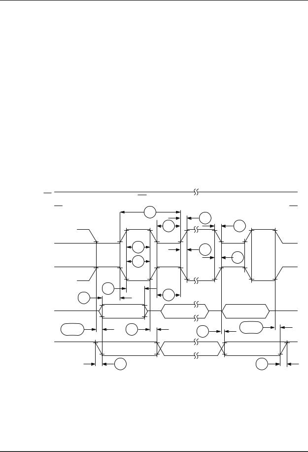
Port A External Bus Synchronous Timing
(VSS = 0 V, VDD = 2.7–3.6 V, TA = –40° to +85°C, CL = 50 pF)
Capacitance Derating
The DSP56824 external bus synchronous timing specifications are designed and tested at the maximum capacitive load of 50 pF, including stray capacitance. Typically, the drive capability of the pins A0–A15, D0–D15, PS, DS, RD, and WR derates linearly at 1.7 ns per 20 pF of additional capacitance from 50 pF to 250 pF of loading. The CLKO pin drive capability is 20 pF. When an internal memory access follows an external memory access, the PS, DS, RD, and WR strobes remain deasserted and A0–A15 do not change from their previous state.
Note: In Figure 2-8 and Figure 2-9, T0, T1, T2, and T3 refer to the internal clock phases and TW refers to wait state.
Table 2-8 External Bus Synchronous Timing
No |
|
|
|
|
|
|
|
|
|
|
|
|
|
|
Characteristic |
Min |
Max |
Unit |
|
|
|
|
|
||||||||||||||
|
|
|
|
|
||||||||||||||
20 |
External Input Clock High to CLKO High |
|
|
ns |
||||||||||||||
|
|
|
|
• |
XCO Asserted High |
3.4 |
13.8 |
|
||||||||||
|
|
|
|
• |
XCO Asserted Low |
9.0 |
18.5 |
|
||||||||||
|
|
|
|
|
||||||||||||||
21 |
CLKO High to A0–A15 Valid |
0.9 |
2.0 |
ns |
||||||||||||||
|
|
|
|
|
|
|
|
|
|
|
|
|
|
|||||
22 |
CLKO High to |
|
|
|
|
|
|
|
|
Valid |
0.3 |
3.1 |
ns |
|||||
PS, |
DS |
|||||||||||||||||
|
|
|
|
|
|
|
|
|
|
|
|
|||||||
23 |
|
CLKO Low to |
|
|
|
|
|
|
|
Asserted Low |
1.1 |
6.4 |
ns |
|||||
WR |
||||||||||||||||||
|
|
|
|
|
|
|
|
|
|
|||||||||
24 |
|
CLKO High to |
|
|
|
|
|
Asserted Low |
0.4 |
4.8 |
ns |
|||||||
RD |
||||||||||||||||||
|
|
|
|
|
||||||||||||||
25 |
CLKO High to D0–D15 Out Valid |
0.9 |
3.1 |
ns |
||||||||||||||
|
|
|
|
|
||||||||||||||
26 |
CLKO High to D0–D15 Out Invalid |
4.4 |
11.2 |
ns |
||||||||||||||
|
|
|
|
|
||||||||||||||
27 |
D0–D15 In Valid to CLKO Low (Setup) |
15.4 |
— |
ns |
||||||||||||||
|
|
|
|
|
||||||||||||||
28 |
CLKO Low to D0–D15 Invalid (Hold) |
0.7 |
— |
ns |
||||||||||||||
|
|
|
|
|
|
|
|
|||||||||||
29 |
CLKO Low to |
|
|
|
|
|
|
Deasserted |
1.9 |
— |
ns |
|||||||
WR |
||||||||||||||||||
|
|
|
|
|
|
|
|
|||||||||||
30 |
|
CLKO Low to |
|
|
|
|
Deasserted |
1.8 |
— |
ns |
||||||||
RD |
||||||||||||||||||
|
|
|
|
|
|
|
|
|||||||||||
31 |
|
|
|
Hold Time from CLKO Low |
0.2 |
— |
ns |
|||||||||||
|
WR |
|||||||||||||||||
|
|
|
|
|
|
|
||||||||||||
32 |
|
|
Hold Time from CLKO Low |
0.2 |
— |
ns |
||||||||||||
|
RD |
|||||||||||||||||
|
|
|
|
|
|
|||||||||||||
33 |
|
CLKO High to D0–D15 Out Active |
–1.3 |
0.6 |
ns |
|||||||||||||
|
|
|
|
|
|
|
|
|
|
|
|
|
|
|
|
|
|
|
PRELIMINARY
MOTOROLA DSP56824 Technical Data Sheet 2-9

Specifications
AC Electrical Characteristics
Table 2-8 External Bus Synchronous Timing (Continued)
No |
|
|
|
|
Characteristic |
Min |
Max |
Unit |
|
|
|
|
|
||||
|
|
|
|
|
||||
34 |
CLKO High to D0–D15 Out Tri-state |
— |
0.3 |
ns |
||||
|
|
|
|
|
||||
35 |
CLKO High to A0–A15 Invalid |
–0.9 |
–2.6 |
ns |
||||
|
|
|
|
|
|
|
|
|
36 |
CLKO High to |
|
|
|
Invalid |
–0.7 |
–1.7 |
ns |
PS, |
DS |
|||||||
|
|
|
|
|
|
|
|
|
Internal Clock Phases
T0 |
T1 |
T2 |
T3 |
T0 |
T1 |
T2 |
T3 |
T0 |
External |
|
|
|
|
|
|
|
|
Clock |
|
|
|
|
|
|
|
|
(Input) |
|
|
|
|
|
|
|
|
|
20 |
|
|
|
|
|
|
|
CLKO |
|
|
|
|
|
|
|
|
(Output) |
|
|
|
|
|
|
|
|
21 |
|
|
|
|
35 |
|
|
|
A0–A15 |
|
|
|
|
|
|
|
|
(See Note) |
|
|
|
|
|
|
|
|
22 |
|
|
|
|
36 |
|
|
|
PS, DS |
|
|
23 |
|
|
WR |
|
|
(Output) |
|
|
24 |
29 |
|
31 |
||
|
||
RD |
|
|
(Output) |
30 |
|
|
||
|
32 |
|
25 |
26 |
|
D0–D15 |
Data Out |
|
(Output) |
||
|
||
33 |
34 |
|
|
27 |
|
D0–D15 |
28 |
|
Data In |
||
(Input) |
||
|
Note: |
During Read-Modify-Write instructions and internal instructions, the address lines do not |
change state.
AA1450
Figure 2-8 Synchronous Timing—No Wait State
PRELIMINARY
2-10 |
DSP56824 Technical Data Sheet |
MOTOROLA |
|
|
|
|
|
|
|
|
|
Specifications |
|
|
|
|
|
|
|
AC Electrical Characteristics |
||
|
Internal Clock Phases |
|
|
|
|
|
|
||
External |
T0 |
T1 |
T2 |
TW |
T2 |
TW |
T2 |
T3 |
T0 |
|
|
|
|
|
|
|
|
|
|
Clock |
|
|
|
|
|
|
|
|
|
(Input) |
|
|
|
|
|
|
|
|
|
|
|
20 |
|
|
|
|
|
|
|
CLKO |
|
|
|
|
|
|
|
|
|
(Output) |
|
|
|
|
|
|
|
|
|
|
|
21 |
|
|
|
|
|
35 |
|
A0–A15 |
|
|
|
|
|
|
|
|
|
(See Note) |
|
|
|
|
|
|
|
|
|
|
22 |
|
|
|
|
|
|
36 |
|
PS, DS |
|
|
|
|
|
|
|
|
|
|
|
23 |
|
|
|
|
|
|
29 |
WR |
|
|
|
|
|
|
|
|
|
(Output) |
|
|
|
|
|
|
|
|
|
|
24 |
|
|
|
|
|
31 |
|
|
RD |
|
|
|
|
|
|
|
|
|
(Output) |
|
|
|
|
|
|
|
30 |
|
|
|
|
|
|
|
|
|
|
|
|
|
25 |
|
|
|
|
32 |
|
26 |
|
|
|
|
|
|
|
|
||
D0–D15 |
|
|
|
|
Data Out |
|
|
|
|
(Output) |
|
|
|
|
|
|
|
||
33 |
|
|
|
|
|
|
34 |
||
|
|
|
|
|
|
28 |
|
||
|
|
|
|
|
|
|
|
|
|
D0–D15 |
|
|
|
|
|
|
|
27 |
|
|
|
|
|
|
|
Data In |
|
||
(Input) |
|
|
|
|
|
|
|
||
|
|
|
|
|
|
|
|
||
Note: |
During Read-Modify-Write instructions and internal instructions, the address lines do not |
||||||||
|
change state. |
|
|
|
|
|
|
|
AA0184 |
|
|
|
|
|
|
|
|
|
|
Figure 2-9 Synchronous Timing—Two Wait States
PRELIMINARY
MOTOROLA |
DSP56824 Technical Data Sheet |
2-11 |

Specifications
AC Electrical Characteristics
Port A External Bus Asynchronous Timing
(VSS = 0 V, VDD = 2.7–3.6 V, TA = –40° to +85°C, CL = 50 pF)
Table 2-9 External Bus Asynchronous Timing
No. |
|
|
|
|
|
|
Characteristic |
Min |
Max |
Unit |
|||||||||||||||||||
|
|
|
|
|
|
|
|
|
|
|
|
|
|
|
|
|
|||||||||||||
|
|
|
|
|
|
|
|
|
|
|
|
|
|
|
|
|
|||||||||||||
40 |
|
Address Valid to |
|
|
|
|
|
|
|
|
|
|
Asserted |
T – 0.5 |
— |
ns |
|||||||||||||
WR |
|||||||||||||||||||||||||||||
|
|
|
|
|
|
|
|
|
|
|
|||||||||||||||||||
41 |
|
|
|
|
|
|
Width Asserted |
|
|
|
|||||||||||||||||||
|
WR |
|
|
|
|||||||||||||||||||||||||
|
|
|
|
|
|
|
• Wait states = 0 |
2T – 6.4 |
— |
ns |
|||||||||||||||||||
|
|
|
|
|
|
|
• Wait states > 0 |
2T(WS + 1) – 6.4 |
— |
ns |
|||||||||||||||||||
|
|
|
|
|
|
|
|
|
|
|
|||||||||||||||||||
42 |
|
|
|
|
|
|
Asserted to D0–D15 Out Valid |
— |
T + 0.7 |
ns |
|||||||||||||||||||
|
WR |
||||||||||||||||||||||||||||
|
|
|
|
|
|
|
|
|
|||||||||||||||||||||
43 |
|
Data Out Hold Time from |
|
|
Deasserted |
T – 5.6 |
— |
ns |
|||||||||||||||||||||
|
WR |
||||||||||||||||||||||||||||
|
|
|
|
|
|
|
|
||||||||||||||||||||||
44 |
|
Data Out Set Up Time to |
|
|
Deasserted |
|
|
|
|||||||||||||||||||||
|
WR |
|
|
|
|||||||||||||||||||||||||
|
|
|
|
|
|
|
• Wait states = 0 |
T + 0.2 |
— |
ns |
|||||||||||||||||||
|
|
|
|
|
|
|
• Wait states > 0 |
T(2WS + 1) + 0.2 |
— |
ns |
|||||||||||||||||||
|
|
|
|
|
|
|
|
|
|
||||||||||||||||||||
45 |
|
|
|
|
|
Deasserted to Address Not Valid |
T – 5.6 |
— |
ns |
||||||||||||||||||||
|
RD |
||||||||||||||||||||||||||||
|
|
|
|
|
|
|
|
|
|
|
|
|
|
|
|||||||||||||||
46 |
|
Address Valid to |
|
|
|
|
|
|
|
|
Deasserted |
3T + 0.3 |
— |
ns |
|||||||||||||||
|
RD |
||||||||||||||||||||||||||||
|
|
|
|
|
|
|
|
|
|
|
|
||||||||||||||||||
47 |
|
Input Data Hold to |
|
|
|
|
|
|
Deasserted |
2.6 |
— |
ns |
|||||||||||||||||
|
RD |
||||||||||||||||||||||||||||
|
|
|
|
|
|
|
|
|
|
||||||||||||||||||||
48 |
|
|
|
|
|
Assertion Width |
|
|
|
||||||||||||||||||||
|
RD |
|
|
|
|||||||||||||||||||||||||
|
|
|
|
|
|
|
• Wait states = 0 |
3T – 5.8 |
— |
ns |
|||||||||||||||||||
|
|
|
|
|
|
|
• Wait states > 0 |
2T(WS) + 3T – 5.8 |
— |
ns |
|||||||||||||||||||
|
|
|
|
|
|
||||||||||||||||||||||||
49 |
|
Address Valid to Input Data Valid |
|
|
|
||||||||||||||||||||||||
|
|
|
|
|
|
|
• Wait states = 0 |
— |
3T – 5.4 |
ns |
|||||||||||||||||||
|
|
|
|
|
|
|
• Wait states > 0 |
— |
2T(WS) + 3T – 5.4 |
ns |
|||||||||||||||||||
|
|
|
|
|
|
|
|
|
|
|
|
||||||||||||||||||
50 |
Address Valid to |
|
|
|
|
|
|
|
|
Asserted |
0.0 |
— |
ns |
||||||||||||||||
RD |
|||||||||||||||||||||||||||||
|
|
|
|
|
|
|
|
|
|
||||||||||||||||||||
51 |
|
|
|
|
|
Asserted to Input Data Valid |
|
|
|
||||||||||||||||||||
|
RD |
|
|
|
|||||||||||||||||||||||||
|
|
|
|
|
|
|
• Wait states = 0 |
— |
3T – 4.7 |
ns |
|||||||||||||||||||
|
|
|
|
|
|
|
• Wait states > 0 |
— |
2T(WS) + 3T – 4.7 |
ns |
|||||||||||||||||||
|
|
|
|
|
|
|
|
|
|
|
|
|
|
||||||||||||||||
52 |
|
|
|
|
|
Deasserted to |
|
|
|
|
|
|
|
Asserted |
T – 0.9 |
— |
ns |
||||||||||||
WR |
RD |
||||||||||||||||||||||||||||
|
|
|
|
|
|
|
|
|
|
|
|
||||||||||||||||||
53 |
|
|
|
Deasserted to |
|
|
|
|
|
|
|
Asserted |
T – 0.8 |
— |
ns |
||||||||||||||
|
RD |
RD |
|||||||||||||||||||||||||||
|
|
|
|
|
|
|
|
|
|
|
|||||||||||||||||||
54 |
|
|
|
|
|
|
Deasserted to |
|
|
|
|
|
|
|
|
Asserted |
2T – 1.0 |
— |
ns |
||||||||||
|
WR |
WR |
|||||||||||||||||||||||||||
|
|
|
|
|
|
|
|
|
|||||||||||||||||||||
55 |
|
|
|
|
Deasserted to |
|
|
|
|
|
|
|
|
|
Asserted |
2T – 0.8 |
— |
ns |
|||||||||||
|
RD |
WR |
|||||||||||||||||||||||||||
|
|
|
|
|
|
||||||||||||||||||||||||
Note: |
|
Timing is both wait state and frequency dependent. In the formulas listed, WS = the number of wait |
|||||||||||||||||||||||||||
|
|
states and T = 1/2 the clock cycle. For 70 MHz operation, T = 7.14 ns. |
|
|
|||||||||||||||||||||||||
|
|
|
|
|
|
|
|
|
|
|
|
|
|
|
|
|
|
|
|
|
|
|
|
|
|
|
|
|
|
PRELIMINARY
2-12 |
DSP56824 Technical Data Sheet |
MOTOROLA |

|
|
|
|
|
|
Specifications |
|
|
|
|
|
|
AC Electrical Characteristics |
A0–A15, |
|
|
|
|
|
|
PS, DS |
|
|
|
|
|
|
(See Note) |
|
|
|
|
46 |
|
|
|
|
|
|
|
|
|
|
|
50 |
|
|
45 |
|
|
|
|
|
53 |
|
|
|
|
|
|
48 |
|
|
|
|
|
|
|
|
RD |
40 |
|
|
|
|
|
|
|
|
|
|
|
|
|
54 |
41 |
52 |
|
|
55 |
WR |
|
|
|
|
|
51 |
|
|
|
|
|
|
|
|
42 |
|
|
49 |
|
|
|
|
44 |
|
43 |
|
47 |
|
|
|
|
|
||
D0–D15 |
|
|
Data Out |
|
|
Data In |
Note: |
During Read-Modify-Write instructions and internal instructions, the address lines do not |
|||||
|
change state. |
|
|
|
|
AA1451 |
|
|
|
|
|
|
|
Figure 2-10 External Bus Asynchronous Timing
PRELIMINARY
MOTOROLA |
DSP56824 Technical Data Sheet |
2-13 |

Specifications
AC Electrical Characteristics
Reset, Stop, Wait, Mode Select, and Interrupt Timing
(VSS = 0 V, VDD = 2.7–3.6 V, TA = –40° to +85°C, CL = 50 pF)
Table 2-10 Reset, Stop, Wait, Mode Select, and Interrupt Timing
|
|
|
|
|
|
|
|
|
|
|
|
|
|
|
|
|
|
|
|
|
|
70 MHz |
|
|
No. |
|
|
|
|
|
|
|
|
|
|
|
|
|
Characteristics |
|
|
Unit |
|||||||
|
|
|
|
|
|
|
|
|
|
|
|
|
Min1 |
Max1 |
||||||||||
|
|
|
|
|
|
|
|
|
|
|
|
|
|
|
|
|
|
|
|
|
|
|
||
|
|
|
|
|
|
|
|
|
|
|||||||||||||||
|
|
|
|
|
|
|
|
|
|
|||||||||||||||
60 |
|
|
|
|
|
Assertion to Address, Data and Control |
4.6 |
14.0 |
ns |
|||||||||||||||
RESET |
||||||||||||||||||||||||
|
|
Signals High Impedance |
|
|
|
|||||||||||||||||||
|
|
|
|
|
|
|
|
|
|
|
|
|
||||||||||||
61 |
|
Minimum |
|
|
|
|
|
|
Assertion Duration2 |
|
|
|
||||||||||||
RESET |
|
|
|
|||||||||||||||||||||
|
|
• OMR Bit 6 = 0 |
524,329 + 38T |
— |
ns |
|||||||||||||||||||
|
|
• OMR Bit 6 = 1 |
38T |
— |
ns |
|||||||||||||||||||
|
|
|
|
|
|
|
|
|
|
|||||||||||||||
62 |
|
Asynchronous |
|
|
|
|
Deassertion to First External |
67T + 4.5 |
67T + 12.3 |
ns |
||||||||||||||
RESET |
||||||||||||||||||||||||
|
|
Address Output 3 |
|
|
|
|||||||||||||||||||
63 |
|
Synchronous Reset Setup Time from |
|
|
|
|
3.8 |
5.6 |
ns |
|||||||||||||||
RESET |
||||||||||||||||||||||||
|
|
Deassertion to CLKO Low |
|
|
|
|||||||||||||||||||
|
|
|
|
|
|
|||||||||||||||||||
64 |
|
Synchronous Reset Delay Time from CLKO High to |
66T + 2.5 |
66T + 7.5 |
ns |
|||||||||||||||||||
|
|
the First External Access3 |
|
|
|
|||||||||||||||||||
65 |
|
Mode and |
|
|
|
|
|
|
Select Setup Time |
0.3 |
— |
ns |
||||||||||||
XCOLF |
||||||||||||||||||||||||
|
|
|
|
|
|
|
|
|
|
|
||||||||||||||
66 |
|
Mode and |
|
|
|
|
|
|
Select Hold Time |
0 |
— |
ns |
||||||||||||
XCOLF |
||||||||||||||||||||||||
|
|
|
|
|
|
|||||||||||||||||||
67 |
|
Edge-sensitive Interrupt Request Width |
2T + 3.8 |
— |
ns |
|||||||||||||||||||
|
|
|
|
|
|
|
|
|
|
|
||||||||||||||
68 |
|
|
|
|
|
|
|
|
Assertion to External Data Memory |
28 + 2.5 |
— |
ns |
||||||||||||
IRQA, |
IRQB |
|||||||||||||||||||||||
|
|
Access Out Valid, caused by first instruction |
|
|
|
|||||||||||||||||||
|
|
execution in the interrupt service routine |
|
|
|
|||||||||||||||||||
|
|
|
|
|
|
|
|
|
|
|||||||||||||||
69 |
|
|
|
|
|
|
|
Assertion to General Purpose Output |
31T + 3.7 |
— |
ns |
|||||||||||||
IRQA, |
IRQB |
|||||||||||||||||||||||
|
|
Valid, caused by first instruction execution in the |
|
|
|
|||||||||||||||||||
|
|
interrupt service routine |
|
|
|
|||||||||||||||||||
|
|
|
|
|
|
|
|
|
|
|||||||||||||||
70 |
|
Synchronous setup time from |
|
|
|
assertion |
1.9 |
2T |
ns |
|||||||||||||||
IRQA, |
IRQB |
|||||||||||||||||||||||
|
|
to Synchronous CLKO High4, 5 |
|
|
|
|||||||||||||||||||
71 |
|
CLKO Low to First Interrupt Vector Address Out |
24T + 4.4 |
— |
ns |
|||||||||||||||||||
|
|
Valid after Synchronous recovery from Wait State6 |
|
|
|
|||||||||||||||||||
72 |
|
|
Width Assertion to Recover from Stop State7 |
2T + 3.8 |
— |
ns |
||||||||||||||||||
IRQA |
||||||||||||||||||||||||
|
|
|
|
|
|
|
|
|||||||||||||||||
73 |
|
Delay from |
|
|
|
|
Assertion to Fetch of first |
|
|
|
||||||||||||||
IRQA |
|
|
|
|||||||||||||||||||||
|
|
instruction (exiting Stop) 2 |
|
|
|
|||||||||||||||||||
|
|
• OMR Bit 6 = 0 |
524,329T |
— |
ns |
|||||||||||||||||||
|
|
• OMR Bit 6 = 1 |
22T |
— |
ns |
|||||||||||||||||||
|
|
|
|
|
|
|
|
|
|
|
|
|
|
|
|
|
|
|
|
|
|
|
|
|
PRELIMINARY
2-14 |
DSP56824 Technical Data Sheet |
MOTOROLA |

Specifications
AC Electrical Characteristics
Table 2-10 Reset, Stop, Wait, Mode Select, and Interrupt Timing (Continued)
|
|
|
|
|
|
|
|
|
70 MHz |
|
|
|
No. |
|
|
Characteristics |
|
|
|
Unit |
|||||
|
|
Min1 |
|
Max1 |
||||||||
|
|
|
|
|
|
|
|
|
|
|
||
|
|
|
|
|
|
|
|
|
||||
|
|
|
|
|
|
|
|
|
||||
74 |
Duration for Level Sensitive |
|
|
Assertion to Cause |
|
|
|
|
||||
IRQA |
|
|
|
|
||||||||
|
the Fetch of First |
IRQA |
Interrupt Instruction (exiting |
|
|
|
|
|||||
|
Stop)2 |
|
|
|
|
|
|
|
|
|
|
|
|
• |
OMR Bit 6 = 0 |
524,329T |
|
— |
ns |
||||||
|
• |
OMR Bit 6 = 1 |
22T |
|
— |
ns |
||||||
|
|
|
|
|
|
|
|
|||||
75 |
Delay from Level Sensitive |
|
|
Assertion to First |
|
|
|
|
||||
IRQA |
|
|
|
|
||||||||
|
Interrupt Vector Address Out Valid (exiting Stop)2 |
|
|
|
|
|||||||
|
• |
OMR Bit 6 = 0 |
524,336T + 2.5 |
|
— |
ns |
||||||
|
• |
OMR Bit 6 = 1 |
22T + 2.5 |
|
— |
ns |
||||||
|
|
|
|
|
|
|
|
|
|
|
|
|
Notes: 1. In the formulas, T = 1/2 the clock cycle and WS = the number of wait states. For an internal frequency of 70 MHz, T = 7.14 ns.
2. Circuit stabilization delay is required during reset when using an external clock or crystal oscillator in two cases:
• After power-on reset
• When recovering from Stop state
3. The instruction fetch is visible on the pins only in Mode 2 and Mode 3.
4. Timing No. 72 is for all IRQx interrupts, while timing No. 73 is only when exiting the Wait state. 5. Timing No. 72 triggers off T0 in the Normal state and off phi0 when exiting the Wait state.
6. The minimum is specified for the duration of an edge-sensitive IRQA interrupt required to recover from the Stop state. This is not the minimum required so that the IRQA interrupt is accepted.
7. The interrupt instruction fetch is visible on the pins only in Mode 3.
PRELIMINARY
MOTOROLA |
DSP56824 Technical Data Sheet |
2-15 |

Specifications
AC Electrical Characteristics
RESET |
|
|
|
61 |
|
60 |
62 |
|
A0–A15, |
First Fetch |
|
D0–D15 |
||
|
||
PS, DS, |
First Fetch |
|
RD, WR |
||
|
AA1452
Figure 2-11 Asynchronous Reset Timing
CLKO |
|
|
|
63 |
|
RESET |
|
|
|
64 |
|
A0–A15, |
|
|
PS, DS, |
|
|
RD, WR |
|
|
|
AA0187 |
|
|
Figure 2-12 Synchronous Reset Timing |
|
RESET |
|
|
|
65 |
|
MODA, |
66 |
|
IRQA, |
||
MODB, |
||
IRQB, |
||
XCOLF |
||
PB15 |
||
|
||
|
AA0188 |
Figure 2-13 Operating Mode Select Timing
IRQA,
IRQB
67
AA0189
Figure 2-14 External Interrupt Timing (Negative-Edge-Sensitive)
PRELIMINARY
2-16 |
DSP56824 Technical Data Sheet |
MOTOROLA |

Specifications
A0–A15,
PS, DS,
RD, WR
IRQA,
IRQB
General
Purpose
I/O Pin
IRQA,
IRQB
CLKO
IRQA,
IRQB
A0–A15, PS, DS, RD, WR
AC Electrical Characteristics
First Interrupt Instruction Execution
68
a) First Interrupt Instruction Execution
69
b) General Purpose I/O |
AA0190 |
Figure 2-15 External Level-Sensitive Interrupt Timing
T0, T2 |
T1, T3 |
|
phi1 |
||
phi0 |
||
|
||
70 |
|
71
First Interrupt Vector
Instruction Fetch
AA0191
Figure 2-16 Synchronous Interrupt from Wait State Timing
PRELIMINARY
MOTOROLA |
DSP56824 Technical Data Sheet |
2-17 |

Specifications
AC Electrical Characteristics
IRQA
A0–A15, PS, DS, RD, WR
72
73
First Instruction Fetch
Not IRQA Interrupt Vector
AA0192
Figure 2-17 Recovery from Stop State Using Asynchronous Interrupt Timing
74
IRQA
75
A0–A15
PS, DS,
RD, WR
First IRQA Interrupt
Instruction Fetch
AA0193
Figure 2-18 Recovery from Stop State Using IRQA Interrupt Service
PRELIMINARY
2-18 |
DSP56824 Technical Data Sheet |
MOTOROLA |

Specifications
AC Electrical Characteristics
Port B and C Pin GPIO Timing
(VSS = 0 V, VDD = 2.7–3.6 V, TA = –40° to +85°C, CL = 50 pF)
Table 2-11 GPIO Timing
No. |
Characteristics |
Min1 |
Max1 |
Unit |
|
|
|
|
|
|
|
|
|
|
80 |
CLKO high to GPIO out valid (GPIO out delay time)2 |
— |
10.7 |
ns |
81 |
CLKO high to GPIO out not valid (GPIO out hold time) |
1.5 |
— |
ns |
|
|
|
|
|
82 |
GPIO in valid to CLKO high (GPIO in set-up time) |
7.8 |
— |
ns |
|
|
|
|
|
83 |
CLKO high to GPIO in not valid (GPIO in hold time) |
0.5 |
— |
ns |
|
|
|
|
|
84 |
Fetch to CLKO high before GPIO change |
12T – 1.7 |
— |
ns |
|
|
|
|
|
85 |
Port B interrupt pulse width |
4T |
— |
ns |
|
|
|
|
|
86 |
Port B interrupt assertion to external data memory access |
|
|
|
|
out valid, caused by first instruction execution in the |
19T + 9.6 |
— |
ns |
|
interrupt service routine |
|
|
|
|
|
|
|
|
87 |
Port B interrupt assertion to general purpose output valid, |
|
|
|
|
caused by first instruction execution in the interrupt service |
31T + 10.8 |
— |
ns |
|
routine |
|
|
|
|
|
|
|
|
Notes: 1. In the formulas, T = 1/2 the clock cycle. For an internal frequency of 70 MHz, T = 7.14 ns.
2. If a 10 kΩ pullup or pulldown resistor is connected to XCOLF/PB15, add 3.9 ns for timings on XCOLF/PB15.
PRELIMINARY
MOTOROLA |
DSP56824 Technical Data Sheet |
2-19 |

Specifications
AC Electrical Characteristics
CLKO |
|
|
(Output) |
|
|
|
80 |
|
|
81 |
|
GPIO |
|
|
(Output) |
|
|
|
82 |
|
|
83 |
|
GPIO |
VALID |
|
(Input) |
||
|
||
A0–A15 |
|
|
|
84 |
Port B
GPIO
Interrupt
(Input)
Fetch the instruction MOVE X0,X:(R0); X0 contains the new value of GPIO
and R0 contains the address of GPIO data register.
AA0194
Figure 2-19 GPIO Timing
85
AA0195
Figure 2-20 Port B Interrupt Timing (Negative-Edge-Sensitive)
PRELIMINARY
2-20 |
DSP56824 Technical Data Sheet |
MOTOROLA |
Specifications
AC Electrical Characteristics
A0–A15,
PS, DS, First Interrupt Instruction Execution
RD, WR
Port B |
86 |
GPIO |
|
Interrupt |
|
(Input) |
|
a) First Interrupt Instruction Execution
General
Purpose
I/O Pin
87
Port B
GPIO Interrupt (Input)
b) General Purpose I/O |
AA0196 |
Figure 2-21 Port B GPIO Interrupt Timing
PRELIMINARY
MOTOROLA |
DSP56824 Technical Data Sheet |
2-21 |

Specifications
AC Electrical Characteristics
Serial Peripheral Interface (SPI) Timing
(VSS = 0 V, VDD = 2.7–3.6 V, TA = –40° to +85°C)
|
|
Table 2-12 |
SPI Timing |
|
|
|
|
||
|
|
|
|
|
|
|
|
|
|
|
|
|
|
|
|
70 MHz |
|
|
|
|
|
|
|
|
|
|
|
||
No. |
|
Characteristic |
|
20 pF Output Load |
50 pF Output Load |
Unit |
|||
|
|
|
|
|
|
|
|
|
|
|
|
|
|
Min |
|
Max |
Min |
Max |
|
|
|
|
|
|
|
|
|
|
|
|
|
|
|
|
|
|
|
|
|
90 |
Cycle time |
|
|
|
|
|
|
|
|
|
• |
Master |
|
100 |
|
— |
100 |
— |
ns |
|
• |
Slave |
|
100 |
|
— |
100 |
— |
ns |
|
|
|
|
|
|
|
|
|
|
91 |
Enable lead time |
|
|
|
|
|
|
|
|
|
• |
Master |
|
— |
|
— |
— |
— |
ns |
|
• |
Slave |
|
6.8 |
|
— |
25 |
— |
ns |
|
|
|
|
|
|
|
|
|
|
92 |
Enable lag time |
|
|
|
|
|
|
|
|
|
• |
Master |
|
— |
|
— |
— |
— |
ns |
|
• |
Slave |
|
6.5 |
|
— |
100 |
— |
ns |
|
|
|
|
|
|
|
|
|
|
93 |
Clock (SCK) high time |
|
|
|
|
|
|
ns |
|
|
• |
Master |
|
17.6 |
|
— |
17.6 |
— |
ns |
|
• |
Slave |
|
25 |
|
— |
25 |
— |
|
|
|
|
|
|
|
|
|
|
|
94 |
Clock (SCK) low time |
|
|
|
|
|
|
|
|
|
• |
Master |
|
24.1 |
|
— |
24.1 |
— |
ns |
|
• |
Slave |
|
25 |
|
— |
25 |
— |
ns |
|
|
|
|
|
|
|
|
|
|
95 |
Data setup time (inputs) |
|
|
|
|
|
|
|
|
|
• |
Master |
|
15.6 |
|
— |
20 |
— |
ns |
|
• |
Slave |
|
–3.2 |
|
— |
0 |
— |
ns |
|
|
|
|
|
|
|
|
|
|
96 |
Data hold time (inputs) |
|
|
|
|
|
|
|
|
|
• |
Master |
|
0 |
|
— |
0 |
— |
ns |
|
• |
Slave |
|
0 |
|
— |
0 |
— |
ns |
|
|
|
|
|
|
|
|
|
|
97 |
Access time (time to data active from |
|
|
|
|
|
|
|
|
|
high-impedance state) |
|
|
|
|
|
|
ns |
|
|
• |
Slave |
|
4.8 |
|
10.7 |
4.8 |
15 |
ns |
|
|
|
|
|
|
|
|
|
|
98 |
Disable time (hold time to high- |
|
|
|
|
|
|
|
|
|
impedance state) |
|
|
|
|
|
|
ns |
|
|
• |
Slave |
|
3.7 |
|
15.2 |
3.7 |
15.2 |
ns |
|
|
|
|
|
|
|
|
|
|
99 |
Data Valid |
|
|
|
|
|
|
|
|
|
• |
Master |
|
4.5 |
|
3.5 |
4.5 |
3.5 |
ns |
|
• Slave (after enable edge) |
|
4.6 |
|
20.4 |
4.6 |
20.4 |
ns |
|
|
|
|
|
|
|
|
|
|
|
PRELIMINARY
2-22 DSP56824 Technical Data Sheet MOTOROLA
Specifications
AC Electrical Characteristics
|
|
Table 2-12 |
SPI Timing (Continued) |
|
|
|
||
|
|
|
|
|
|
|
|
|
|
|
|
|
|
70 MHz |
|
|
|
|
|
|
|
|
|
|
|
|
No. |
|
Characteristic |
|
20 pF Output Load |
50 pF Output Load |
Unit |
||
|
|
|
|
|
|
|
|
|
|
|
|
|
Min |
Max |
Min |
Max |
|
|
|
|
|
|
|
|
|
|
|
|
|
|
|
|
|
|
|
100 |
Data invalid |
|
|
|
|
|
|
|
|
• |
Master |
|
0 |
— |
0 |
— |
ns |
|
• |
Slave |
|
0 |
— |
0 |
— |
ns |
|
|
|
|
|
|
|
|
|
101 |
Rise time |
|
|
|
|
|
|
|
|
• |
Master |
|
4.1 |
5.5 |
4.1 |
11.5 |
ns |
|
• |
Slave |
|
0 |
4.0 |
0 |
10.0 |
ns |
|
|
|
|
|
|
|
|
|
102 |
Fall time |
|
|
|
|
|
|
|
|
• |
Master |
|
1.5 |
4.7 |
2.0 |
9.7 |
ns |
|
• |
Slave |
|
0 |
4.0 |
2.0 |
9.0 |
ns |
|
|
|
|
|
|
|
|
|
SS |
SS is held High on master |
|
(Input) |
||
|
||
|
90 |
|
|
|
|
101 |
|
SCK (CPL = 0) |
|
|
94 |
|
102 |
See |
|
|
|
|
|
(Output) |
Note |
|
|
|
|
|
|
93 |
|
102 |
|
|
|
|
|
|
|
|
|
94 |
|
|
101 |
|
|
|
|
|
|
SCK (CPL = 1) |
See |
|
|
|
|
(Output) |
Note |
|
|
|
|
|
|
96 |
93 |
|
|
|
95 |
|
|
|
|
|
|
|
|
|
|
MISO |
|
MSB in |
Bits 6–1 |
|
LSB in |
(Input) |
|
|
|||
|
|
|
|
|
|
|
99 (ref) |
100 |
|
99 |
100 (ref) |
|
|
|
|||
|
|
|
|
|
|
MOSI |
Master MSB out |
Bits 6–1 |
Master LSB out |
|
(Output) |
|||||
|
|
|
|||
|
|
102 |
|
101 |
|
Note: |
This first clock edge is generated internally, but is not seen at the SCK pin. |
||||
AA0197
Figure 2-22 SPI Master Timing (CPH = 0)
PRELIMINARY
MOTOROLA |
DSP56824 Technical Data Sheet |
2-23 |

Specifications
AC Electrical Characteristics
|
SS |
|
|
|
|
|
SS is held High on master |
||||
(Input) |
|||||
|
|
||||
|
90 |
|
102 |
|
|
|
|
|
|
|
94 |
|
|
101 |
SCK (CPL = 0) |
|
|
|
See |
(Output) |
|
|
|
Note |
|
93 |
|
|
102 |
|
|
|
|
|
|
94 |
|
|
|
SCK (CPL = 1) |
|
|
|
See |
(Output) |
|
|
|
Note |
|
93 |
|
|
95 |
|
|
101 |
|
|
|
|
|
96 |
|
|
|
|
|
|
MISO |
MSB in |
Bits 6–1 |
|
LSB in |
(Input) |
|
|||
|
|
|
|
|
99 (ref) |
100 |
|
99 |
100(ref) |
|
|
|||
|
|
|
|
|
MOSI |
Master MSB out |
Bits 6 – 1 |
Master LSB out |
|
(Output) |
|
||||
|
|
|
|
||
|
|
102 |
|
101 |
|
Note: |
This last clock edge is generated internally, but is not seen at the SCK pin. |
AA0198 |
|||
Figure 2-23 SPI Master Timing (CPH = 1)
PRELIMINARY
2-24 |
DSP56824 Technical Data Sheet |
MOTOROLA |

Specifications
AC Electrical Characteristics
SS
(Input)
SCK (CPL = 0) (Input)
SCK (CPL = 1) (Input)
MISO (Output)
MOSI (Input)
|
90 |
|
102 |
92 |
|
|
|
|
|
|
|
|
94 |
|
101 |
|
|
93 |
|
|
|
|
|
91 |
|
|
|
|
|
94 |
|
|
|
|
|
97 |
93 |
101 |
|
102 |
98 |
|
|
||||
|
|
|
|
|
|
Slave MSB out |
|
Bits 6–1 |
Slave LSB out |
See |
|
|
Note |
||||
|
|
|
|
|
|
95 |
|
99 |
100 |
|
100 |
|
96 |
|
|
||
|
|
|
|
|
|
MSB in |
Bits 6–1 |
LSB in |
Note: |
Not defined, but normally MSB of character just received |
AA0199 |
Figure 2-24 SPI Slave Timing (CPH = 0)
PRELIMINARY
MOTOROLA |
DSP56824 Technical Data Sheet |
2-25 |

Specifications
AC Electrical Characteristics
SS
(Input)
CK (CPL = 0) (Input)
CK (CPL = 1) (Input)
MISO (Output)
MOSI (Input)
|
90 |
|
102 |
|
|
94 |
101 |
|
|
|
|
|
||
|
91 |
93 |
92 |
|
|
94 |
|||
|
|
|
||
99 |
93 |
|
101 |
|
|
|
|||
97 |
102 |
98 |
||
|
||||
See |
Slave MSB out |
Bits 6–1 |
Slave LSB out |
|
Note |
||||
|
|
|
||
95 |
|
99 |
100 |
|
|
|
96 |
||
|
|
|
||
|
MSB in |
Bits 6–1 |
LSB in |
Note: |
Not defined, but normally LSB of character previously transmitted |
AA0200 |
Figure 2-25 SPI Slave Timing (CPH = 1)
PRELIMINARY
2-26 |
DSP56824 Technical Data Sheet |
MOTOROLA |

Specifications
AC Electrical Characteristics
Synchronous Serial Interfaces (SSI) Timing
(VSS = 0 V, VDD = 2.7–3.6 V, TA = –40° to +85°C, CL = 50 pF)
Table 2-13 SSI Timing
No. |
|
Characteristic |
70 MHz |
Case1 |
Unit |
|
|
|
|
||||
|
Min |
Max |
||||
|
|
|
|
|
||
|
|
|
|
|
|
|
|
|
|
|
|
|
|
|
|
Internal Clock Operation |
|
|
|
|
|
|
|
|
|
|
|
110 |
Clock cycle2 |
|
100 |
— |
i ck |
ns |
111 |
Clock high period |
|
33.2 |
— |
i ck |
ns |
|
|
|
|
|
|
|
112 |
Clock low period |
|
30.6 |
— |
i ck |
ns |
|
|
|
|
|
|
|
113 |
Output clock rise/fall time |
— |
7.5 |
i ck |
ns |
|
|
|
|
|
|
|
|
114 |
STCK high to STFS (bl) high3 |
1.8 |
9.7 |
i ck |
ns |
|
115 |
SRCK high to SRFS (bl) high3 |
1.3 |
10 |
i ck |
ns |
|
116 |
STCK high to STFS (bl) low3 |
–2.9 |
8 |
i ck |
ns |
|
117 |
SRCK high to SRFS (bl) low3 |
–2.7 |
8.7 |
i ck |
ns |
|
118 |
SRD setup time before SRCK low |
9 |
— |
i ck |
ns |
|
|
|
|
|
|
|
|
119 |
SRD hold time after SRCK low |
0 |
— |
i ck |
ns |
|
|
|
|
|
|
|
|
120 |
STCK high to STFS (wl) high3 |
13.8 |
24.4 |
i ck |
ns |
|
121 |
SRCK high to SRFS (wl) high3 |
14.5 |
25.9 |
i ck |
ns |
|
122 |
STCK high to STFS (wl) low3 |
–2.9 |
9.0 |
i ck |
ns |
|
123 |
SRCK high to SRFS (wl) low3 |
–2.2 |
10.6 |
i ck |
ns |
|
124 |
STCK high to STD enable from high impedance |
1.5 |
1.7 |
i ck |
ns |
|
|
|
|
|
|
|
|
125 |
STCK high to STD valid |
–3.4 |
7.9 |
i ck |
ns |
|
|
|
|
|
|
|
|
126 |
STCK High to STD not valid |
–5.7 |
0.7 |
i ck |
ns |
|
|
|
|
|
|
|
|
127 |
STCK high to STD high impedance |
6.8 |
11.3 |
i ck |
ns |
|
|
|
|
|
|
|
|
|
|
External Clock Operation |
|
|
|
|
|
|
|
|
|
|
|
128 |
Clock cycle2 |
|
100 |
— |
x ck |
ns |
129 |
Clock high period |
|
50 |
— |
x ck |
ns |
|
|
|
|
|
|
|
130 |
Clock low period |
|
50 |
— |
x ck |
ns |
|
|
|
|
|
|
|
132 |
SRD Setup time before SRCK low |
–8.7 |
— |
x ck |
ns |
|
|
|
|
|
|
|
|
133 |
SRD hold time after SRCK low4 |
1.7 |
— |
x ck |
ns |
|
|
|
PRELIMINARY |
|
|
|
|
|
|
|
|
|
|
|
MOTOROLA |
DSP56824 Technical Data Sheet |
|
|
2-27 |
||

Specifications
AC Electrical Characteristics
Table 2-13 SSI Timing (Continued)
No. |
|
Characteristic |
70 MHz |
Case1 |
Unit |
||
|
|
|
|
||||
|
Min |
|
Max |
||||
|
|
|
|
|
|
||
|
|
|
|
|
|
|
|
|
|
|
|
|
|
|
|
134 |
|
STCK high to STFS (bl) high3 |
0.4 |
|
100 |
x ck |
ns |
135 |
|
SRCK high to SRFS (bl) high3 |
0.5 |
|
100 |
x ck |
ns |
136 |
|
STCK high to STFS (bl) low3 |
0 |
|
99 |
x ck |
ns |
137 |
|
SRCK high to SRFS (bl) low3 |
0 |
|
99 |
x ck |
ns |
138 |
|
STCK high to STFS (wl) high3 |
0.4 |
|
100 |
x ck |
ns |
139 |
|
SRCK high to SRFS (wl) high3 |
0.5 |
|
100 |
x ck |
ns |
140 |
|
STCK high to STFS (wl) low3 |
0 |
|
99 |
x ck |
ns |
141 |
|
SRCK high to SRFS (wl) low3 |
0 |
|
99 |
x ck |
ns |
142 |
|
STCK high to STD enable from high impedance |
7.8 |
|
19 |
x ck |
ns |
|
|
|
|
|
|
|
|
143 |
|
STCK high to STD valid |
11.7 |
|
28.5 |
x ck |
ns |
|
|
|
|
|
|
|
|
144 |
|
STCK high to STD not valid |
5.8 |
|
21.1 |
x ck |
ns |
|
|
|
|
|
|
|
|
145 |
|
STCK high to STD high impedance |
9.2 |
|
22.9 |
x ck |
ns |
|
|
|
|
|
|
|
|
|
|
Synchronous Internal Clock Operation |
|
|
|
||
|
|
(in addition to standard internal clock parameters) |
|
|
|
||
|
|
|
|
|
|
|
|
146 |
|
SRD setup before STCK falling |
18.4 |
|
— |
i ck s |
ns |
|
|
|
|
|
|
|
|
147 |
|
SRD hold after STCK falling4 |
0 |
|
— |
i ck s |
ns |
|
|
Synchronous External Clock Operation |
|
|
|
||
|
|
(in addition to standard external clock parameters) |
|
|
|
||
|
|
|
|
|
|
|
|
148 |
|
SRD setup before STCK falling |
–4.7 |
|
— |
x ck s |
ns |
|
|
|
|
|
|
|
|
149 |
|
SRD hold after STCK falling4 |
1.7 |
|
— |
x ck s |
ns |
Notes: 1. |
The following abbreviations are used to represent the various operational cases: |
|
|
||||
|
|
i ck = Internal Clock and Frame Sync |
|
|
|
|
|
|
|
x ck = External Clock and Frame Sync |
|
|
|
|
|
|
|
i ck s = Internal Clock, Synchronous mode (implies that only one frame sync FS is used) |
|
||||
|
|
x ck s = External Clock, Synchronous mode (implies that only one frame sync FS is used) |
|
||||
2. |
All the timings for the SSI are given for a non-inverted serial clock polarity (SCKP = 0 in CRB) and a |
||||||
|
|
non-inverted frame sync (FSI = 0 in CRB). If the polarity of the clock and/or the frame sync have been |
|||||
|
|
inverted, all the timings remain valid by inverting the clock signal SCK and/or the frame sync FSR/ |
|||||
|
|
FST in the tables and in the figures. |
|
|
|
|
|
3. |
bl = bit length; wl = word length. |
|
|
|
|
|
|
|
|
|
|
|
|
|
|
PRELIMINARY
2-28 |
DSP56824 Technical Data Sheet |
MOTOROLA |

Specifications
AC Electrical Characteristics
110 |
|
|
|
113 |
|
|
|
111 |
112 |
|
|
STCK |
|
|
|
Output |
|
|
|
114 |
116 |
|
|
STFS (bl) |
|
|
|
Output |
|
|
|
|
120 |
122 |
|
STFS (wl) |
|
|
|
Output |
126 |
|
|
|
|
||
|
125 |
127 |
|
|
|
||
STD |
124 |
|
|
First Bit |
Last Bit |
||
Output |
|||
|
|
||
|
147 |
|
|
|
146 |
|
|
SRD |
First Bit |
Last Bit |
|
Input |
|||
|
|
Note: |
SRD Input in Synchronous mode only |
AA0201 |
|
|
Figure 2-26 SSI Transmitter Internal Clock Timing
PRELIMINARY
MOTOROLA |
DSP56824 Technical Data Sheet |
2-29 |

Specifications
AC Electrical Characteristics
|
128 |
|
|
129 |
130 |
|
|
STCK |
|
|
|
Input |
|
|
|
134 |
136 |
|
|
STFS (bl) |
|
|
|
Input |
|
|
|
|
138 |
140 |
|
STFS (wl) |
|
|
|
Input |
144 |
|
|
|
|
||
|
143 |
145 |
|
|
|
||
STD |
142 |
|
|
First Bit |
Last Bit |
||
Output |
|||
|
|
||
|
|
149 |
|
|
148 |
|
|
SRD |
First Bit |
Last Bit |
|
Input |
|||
|
|
Note: |
SRD Input in Synchronous mode only |
AA0202
Figure 2-27 SSI Transmitter External Clock Timing
PRELIMINARY
2-30 |
DSP56824 Technical Data Sheet |
MOTOROLA |
Specifications
AC Electrical Characteristics
110 |
|
|
|
113 |
|
|
|
111 |
112 |
|
|
SRCK |
|
|
|
Output |
|
|
|
115 |
117 |
|
|
SRFS (bl) |
|
|
|
Output |
|
|
|
|
121 |
123 |
|
SRFS (wl) |
|
|
|
Output |
|
|
|
|
|
119 |
|
|
118 |
|
|
SRD |
First Bit |
Last Bit |
|
Input |
|||
|
|
||
|
|
AA0203 |
|
Figure 2-28 SSI Receiver Internal Clock Timing |
|||
128 |
|
|
|
129 |
130 |
|
|
SRCK |
|
|
|
Input |
|
|
|
135 |
137 |
|
|
SRFS (bl) |
|
|
|
Input |
|
|
|
|
139 |
141 |
|
SRFS (wl) |
|
|
|
Input |
|
133 |
|
|
|
||
|
132 |
|
|
SRD |
First Bit |
Last Bit |
|
Input |
|||
|
|
||
|
|
AA0204 |
|
Figure 2-29 SSI Receiver External Clock Timing
PRELIMINARY
MOTOROLA |
DSP56824 Technical Data Sheet |
2-31 |

Specifications
AC Electrical Characteristics
Timer Timing
(VSS = 0 V, VDD = 2.7–3.6 V, TA = –40° to +85°C, CL = 50 pF)
Table 2-14 Timer Timing
|
|
|
|
|
70 MHz |
|
No. |
|
Characteristic |
|
|
Unit |
|
|
|
|
|
Min |
Max |
|
150 |
Timer input valid to CLKO high (setup time) |
11.4 |
— |
ns |
||
151 |
CLKO high to timer input not valid (hold time) |
0 |
— |
ns |
||
152 |
CLKO high to timer output asserted |
9.5 |
18.7 |
ns |
||
153 |
CLKO high to timer output deasserted |
5.1 |
20.7 |
ns |
||
154 |
Timer input period |
|
8T |
— |
ns |
|
155 |
Timer input high/low period |
|
4T |
— |
ns |
|
CLKO |
|
|
|
|
|
|
(Output) |
|
|
|
|
|
|
|
|
150 |
151 |
|
|
|
TIO01 |
|
|
|
|
|
|
TIO2 |
|
|
|
|
|
|
(Input) |
|
|
|
|
|
|
|
|
|
152 |
|
153 |
|
TIO01 |
|
|
|
|
|
|
TIO2 |
|
|
|
|
|
|
(Output) |
|
|
|
|
|
|
TIO01 |
|
|
|
|
|
|
TIO2 |
|
|
|
|
|
|
(Input) |
154 |
155 |
155 |
|
|
|
AA0205
Figure 2-30 Timer Timing
PRELIMINARY
2-32 |
DSP56824 Technical Data Sheet |
MOTOROLA |

Specifications
AC Electrical Characteristics
JTAG Timing
(VSS = 0 V, VDD = 2.7–3.6 V, TA = –40° to +85°C, CL = 50 pF)
Table 2-15 JTAG Timing
|
|
|
|
|
|
70 MHz |
|
|
No. |
|
|
|
Characteristics |
|
|
|
Unit |
|
|
|
Min |
|
Max |
|||
|
|
|
|
|
|
|
||
|
|
|
|
|
|
|
||
|
|
|
|
|
|
|
||
160 |
|
TCK frequency of operation |
|
|
|
|
||
|
|
|
• |
In OnCE Debug mode (EXTAL/8) |
0.0 |
|
8.75 |
MHz |
|
|
|
• |
In JTAG mode |
0.0 |
|
10 |
MHz |
|
|
|
|
|
|
|
||
161 |
|
TCK cycle time |
100 |
|
— |
ns |
||
|
|
|
|
|
|
|
||
162 |
|
TCK clock pulse width |
50 |
|
— |
ns |
||
|
|
|
|
|
|
|
||
164 |
|
Boundary scan input data setup time |
34.5 |
|
— |
ns |
||
|
|
|
|
|
|
|
||
165 |
|
Boundary scan input data hold time |
0 |
|
— |
ns |
||
|
|
|
|
|
|
|
||
166 |
|
TCK low to output data valid |
— |
|
40.6 |
ns |
||
|
|
|
|
|
|
|
||
167 |
|
TCK low to output tri-state |
— |
|
43.4 |
ns |
||
|
|
|
|
|
|
|
||
168 |
|
TMS, TDI data setup time |
0.4 |
|
— |
ns |
||
|
|
|
|
|
|
|
||
169 |
|
TMS, TDI data hold time |
1.2 |
|
— |
ns |
||
|
|
|
|
|
|
|
||
170 |
|
TCK low to TDO data valid |
— |
|
26.6 |
ns |
||
|
|
|
|
|
|
|
||
171 |
|
TCK low to TDO tri-state |
— |
|
23.5 |
ns |
||
|
|
|
|
|
|
|
|
|
172 |
|
|
|
assertion time |
50 |
|
— |
ns |
|
TRST |
|||||||
|
|
|
|
|
|
|
|
|
173 |
|
|
assertion time |
8T |
|
— |
ns |
|
|
DE |
|||||||
|
|
|
|
|
||||
Note: |
Timing is both wait state and frequency dependent. In the formulas listed, WS = the number of wait |
|||||||
|
states and T = 1/2 the clock cycle. For 70 MHz operation, T = 7.14 ns. |
|
|
|
||||
|
|
|
|
|
|
|
|
|
PRELIMINARY
MOTOROLA |
DSP56824 Technical Data Sheet |
2-33 |

Specifications
AC Electrical Characteristics
|
|
161 |
|
VIH |
162 |
162 |
|
|
|
||
TCK |
VM |
VM |
|
(Input) |
VIL |
|
|
VM = VIL + (VIH – VIL)/2 |
AA1453 |
||
|
Figure 2-31 Test Clock Input Timing Diagram
TCK |
|
|
(Input) |
|
|
|
164 |
165 |
Data |
Input Data Valid |
|
Inputs |
||
|
166 |
|
Data |
|
Output Data Valid |
Outputs |
|
|
|
|
|
167
Data
Outputs
|
166 |
|
Data |
Output Data Valid |
|
Outputs |
||
|
AA0207
Figure 2-32 Boundary Scan (JTAG) Timing Diagram
PRELIMINARY
2-34 |
DSP56824 Technical Data Sheet |
MOTOROLA |

Specifications
TCK (Input)
TDI
TMS (Input)
TDO (Output)
TDO (Output)
TDO (Output)
TRST
(Input)
DE
AC Electrical Characteristics
168 |
169 |
Input Data Valid
170
Output Data Valid
171
170
Output Data Valid
AA0208
Figure 2-33 Test Access Port Timing Diagram
172
AA0209
Figure 2-34 TRST Timing Diagram
173
AA0210
Figure 2-35 OnCE—Debug Event
PRELIMINARY
MOTOROLA |
DSP56824 Technical Data Sheet |
2-35 |

Specifications
AC Electrical Characteristics
PRELIMINARY
2-36 |
DSP56824 Technical Data Sheet |
MOTOROLA |