

Freescale Semiconductor
Application Note
AN1947
Rev. 2, 08/2005
56F800 ADC
Understanding 56F800 ADC Specifications and How to Get the Best Performance in Applications
Bill Hutchings
1. Introduction
This document describes the meaning of the Data Sheet specifications for the Analog-to-Digital Converter (ADC), how they are calculated, and how they relate to real-world signal impairments. In addition, this note introduces simple methods for getting the best performance from the 56F800 ADC and gives an overview of the differences in ADC performance for the various 56F800 components.
2. ADC Transfer Function and Error
Sources
This section describes the ideal transfer function for an ADC. The Data Sheet specifications provide data on how the real ADC transfer function strays from the ideal.
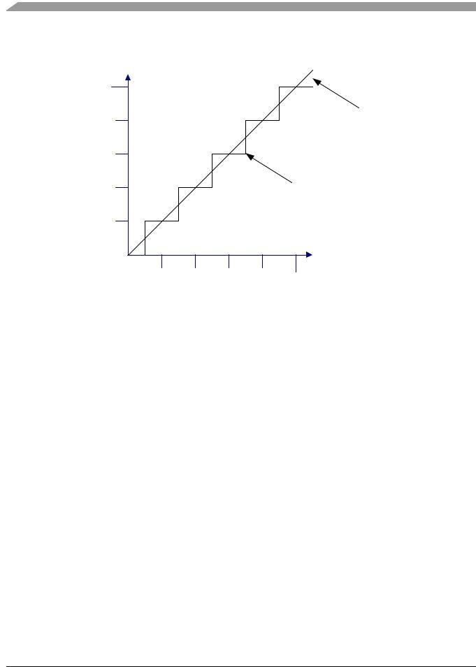
The theoretical ideal transfer function for an ADC is a straight line, but this would require an infinite number of steps, and therefore an infinite number of bits to represent. A practical theoretical transfer function is a uniform linear staircase function, which is shown in Figure 2-1. The Data Sheet ADC specifications describe in quantitative terms how far the component deviates from the ideal transfer function.
© Freescale Semiconductor, Inc., 2004, 2005. All rights reserved.
|
Contents |
|
1. Introduction ........................................... |
1 |
|
2. ADC Transfer Function and Error |
|
|
|
Sources ............................................. |
1 |
2.1 |
Quantization Error........................... |
2 |
2.2 |
Static Errors..................................... |
3 |
2.3 |
Dynamic Errors ............................... |
6 |
2.4 |
Measurement Methods.................... |
7 |
3. Using the 56F800 ADC ......................... |
7 |
|
3.1 |
Input Impedance.............................. |
7 |
3.2 |
Practical ADC Calibration .............. |
9 |
3.3 |
Optimizing Linearity and ENOB .. |
11 |
3.4 |
Choosing the Right Device ........... |
11 |
3.5 |
Using the ADC’s Operational |
|
|
Modes ............................................ |
11 |
4. Conclusion .......................................... |
13 |
|
A. 56F800 ADC Internal Structure .......... |
14 |
|
ADC Transfer Function and Error Sources
Output Code
101 |
|
|
|
|
|
|
|
|
Ideal Transfer |
100 |
|
|
|
Function |
|
|
|
|
|
011 |
|
|
|
|
|
|
|
|
Practical Ideal |
010 |
|
|
|
Transfer |
|
|
|
Function |
|
|
|
|
|
|
001 |
|
|
|
|
|
|
|
|
Analog Input (LSB) |
1 |
2 |
3 |
4 |
5 |
|
Figure 2-1. Transfer Function |
|||
2.1 Quantization Error
The practical ideal transfer function used to represent a continuous analog signal as a set of discrete staircase digital codes introduces quantization error. As Figure 2-1 shows, the width of each step is one code increment, or one Least Significant Bit, so a range of continuous analog inputs is represented by a single code value. The mapping can be represented as seen in Table 2-1.
Table 2-1. Quantization Error
Analog input |
Digital Code |
|
|
|
|
4.5 - 5.5 |
101 |
|
|
3.5 - 4.5 |
100 |
|
|
2.5 - 3.5 |
011 |
|
|
1.5 - 2.5 |
010 |
|
|
0.5 - 1.5 |
001 |
|
|
0 - 0.5 |
000 |
|
|
56F800 ADC, Rev. 2
2 |
Freescale Semiconductor |

Static Errors
If the value 001 represents the mid-point of the analog input range of 0.5 to 1.5, then the analog value 1.0 is represented by 001 with no error. But since the analog value of 0.5 is also represented by the digital value 001, the end points of the analog range represent the maximum error. In terms of bits, the maximum error can be expressed as +1/2 bit for the 0.5 endpoint and -1/2 bit for the 1.5 endpoint. Maximum physical voltage error, ev, can be calculated with the following equation:
ev = (1 LSB voltage range)/2
The voltage range of 1 LSB depends on the full-scale voltage range that the ADC is set to sample and the total number of digital codes present. Analog-to-Digital converters are specified in the number of bits of resolution. If “n” is the number of bits of resolution, then the total number of digital codes present is 2n, so the voltage range represented by each bit vb can be expressed as:
vb = (Full scale voltage range)/2n
The maximum physical voltage error ev can be expressed as: ev = (Full scale voltage range)/2n+1
2.2 Static Errors
Static errors are characterized by offset error, gain error, integral non-linearity and differential non-linearity. While static errors can be fully characterized using non-varying input signals, they affect the conversion of all input signals, whether they are static or dynamic.
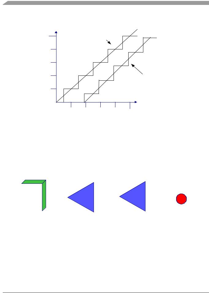
Let us first examine gain and offset errors, shown by Figure 2-2. Looking at the actual transfer function, we see a DC-bias error causing the zero crossing to occur at a point other than the origin. So, the analog input that causes a zero code to be output in this example is 1.5 to 2.5 code instead of 0 to 0.5 code. This offset error is a constant across the entire analog input range. We can see the gain error reflected in the diagram in that the actual transfer function doesn’t have a 45 degree slope. The following equation describes the best-fit linear regression of the actual ADC transfer function.
y = ( EGAIN x ) + VOFFSET
EGAIN = Gain error value from the component Data Sheet x = Actual analog input
VOFFSET = DC input offset voltage from the component Data Sheet y = Apparent analog input converted by ADC
These effects are linear over the input voltages and frequency and demonstrate that the actual analog input voltage can be solved for and the effects of the gain errors and offset voltages can be removed.
56F800 ADC, Rev. 2
Freescale Semiconductor |
3 |
ADC Transfer Function and Error Sources
Output Code |
|
|
|
|
101 |
Practical Ideal |
|
|
|
|
Transfer |
|
|
|
100 |
Function |
|
|
|
|
|
|
|
|
011 |
|
|
|
|
010 |
|
|
|
Actual Transfer |
|
|
|
Function |
|
001 |
|
|
|
|
|
|
|
|
Analog Input (LSB) |
1 |
2 |
3 |
4 |
5 |
Figure 2-2. Gain and Offset Errors
In any given system, the conversion point of interest to an algorithm can be fairly far removed from the analog input of the ADC, as illustrated in Figure 2-3. In these cases, gain and DC voltage offsets can be introduced external to the ADC, so it is often important to take the entire system into account when analyzing the total gain and offset errors. A calibration step may be required, depending on the specific requirements of the end system. In the calibration, known precise and accurate signals are injected into the system and conversions are performed. The actual results of the conversions are compared to the expected values and the error values for gain and offset voltage can be determined. These errors can then be removed digitally in the processor or by trimming the analog circuitry before the analog input into the processor ADC.
|
|
|
|
|
|
|
|
|
|
|
|
|
|
|
|
|
|
|
|
|
|
|
|
|
|
|
|
|
|
|
|
|
Buffering/ |
Buffering/ |
Signal of interest |
||||
56F800 device |
|||||||||
Isolation/Gain |
Isolation/Gain |
||||||||
|
|
|
stage |
stage |
|
|
|||
Figure 2-3. System Gain and Offset Errors
The 56F800 devices have been characterized and most of the gain and offset errors have been removed by internal compensation in the chip. Designers should analyze the gain and offset errors stated in the Data Sheet for the device being implemented and the requirements for the algorithm they are to perform, because it is
56F800 ADC, Rev. 2
4 |
Freescale Semiconductor |
Static Errors
possible that no adjustment is required for proper operation. If it is determined that the gain and offset errors must be compensated for, this is a relatively straightforward proposition because these errors are linear, stable over frequency, and easily characterized.
Integral (INL) and differential non-linearity (DNL) are errors introduced by all ADC units. They are quite difficult to compensate and characterize. In general, a designer will need to determine the required linearity for a particular algorithm and choose the system components accordingly. As with gain and offset errors, integral and differential non-linearity errors can be introduced at any part of the system and are not limited to the ADC.
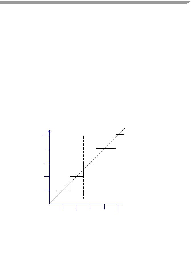
The integral and differential non-linearity errors are closely related to one another. As shown in Figure 2-4, the width of each conversion step of the output code sequence is not the same. This non-uniformity in step width is the source of the differential and integral non-linearity. The differential non-linearity is the difference in width from the ideal case in each step and is measured in LSBs. In the specific case shown in Figure 2-4, the net result of the non-linearities is an under-representation of the code sequences 011 and 101, which have a negative differential non-linearity because the width is less than the ideal 1 LSB bit width. The sequence 100 will be over-represented and has a positive differential non-linearity because the step width is greater than 1 LSB. It is possible in some ADCs that the differential non-linearity will cause output codes to be missing completely or repeated. An ADC’s Monotonicity is guaranteed when the digital output codes increase, or remain the same, with increasing analog input voltage. Monotonicity is guaranteed in the 56F800 components. A maximum differential non-linearity of one 1 LSB or less also ensures a monotonic transfer function with no missing or repeated codes. All 56F800 components have a maximum differential non-linearity of 1 LSB or less.
Output Code
101
100
011
Ideal Transfer
Non linear transfer function
010
001
 Analog Input (LSB)
1 |
2 |
3 |
4 |
5 |
Figure 2-4. Non-linear Static Errors
56F800 ADC, Rev. 2
Freescale Semiconductor |
5 |