

ЦОС_Заочники2013 / Курсовая МПиЦОС 2011 / Справочная информация / ADC&DAC / AD974
.pdfa |
4-Channel, 16-Bit, 200 kSPS |
|
Data Acquisition System |
||
|
|
AD974 |
|
|
|
FEATURES
Fast 16-Bit ADC with 200 kSPS Throughput Four Single-Ended Analog Input Channels Single +5 V Supply Operation
Input Ranges: 0 V to +4 V, 0 V to +5 V and 610 V
120 mW Max Power Dissipation Power-Down Mode 50 mW
Choice of External or Internal 2.5 V Reference On-Chip Clock
Power-Down Mode
GENERAL DESCRIPTION
The AD974 is a four-channel, data acquisition system with a serial interface. The part contains an input multiplexer, a highspeed 16-bit sampling ADC and a +2.5 V reference. All of this operates from a single +5 V power supply that also has a powerdown mode. The part will accommodate 0 V to +4 V, 0 V to +5 V or ±10 V analog input ranges.
The interface is designed for an efficient transfer of data while requiring a low number of interconnects.
The AD974 is comprehensively tested for ac parameters such as SNR and THD, as well as the more traditional parameters of offset, gain and linearity.
The AD974 is fabricated on Analog Devices’ BiCMOS process, which has high performance bipolar devices along with CMOS transistors.
The AD974 is available in 28-lead DIP, SOIC and SSOP packages.
FUNCTIONAL BLOCK DIAGRAM
|
PWRD |
BIP |
CAP |
REF |
VDIG |
VANA |
|
|
|
|
REF |
|
|
2.5V |
|
|
|
|
BUFF |
|
REFERENCE |
|
|
V1A |
RESISTIVE |
|
|
|
|
|
|
|
|
|
|
|
|
|
|
V1B |
NETWORK |
|
AD974 |
|
|
|
|
|
|
|
|
|
|
||
V2A |
|
|
|
|
|
|
EXT/INT |
RESISTIVE |
|
SWITCHED 16 |
|
DATACLK |
|||
|
|
|
|||||
V2B |
NETWORK |
|
|
||||
4 TO 1 |
CAP ADC |
|
|
DATA |
|||
|
|
SERIAL |
|||||
|
|
|
|
||||
|
|
MUX |
|
|
INTERFACE |
R/C |
|
|
|
+ |
|
|
|||
V3A |
RESISTIVE |
|
|
|
|
||
LATCH |
|
|
|
|
|
||
|
|
|
|
|
CS |
||
V3B |
NETWORK |
|
|
|
|
|
|
|
|
|
|
|
|
||
|
|
|
CLOCK |
|
|
|
SYNC |
V4A |
RESISTIVE |
EN |
|
CONTROL LOGIC |
|
||
V4B |
NETWORK |
|
|
|
|||
|
|
|
|
|
& |
|
|
|
|
|
CALIBRATION CIRCUITRY |
|
|||
|
AGND1 AGND2 |
A0 A1 WR1 WR2 |
|
BUSY |
DGND |
|
|
PRODUCT HIGHLIGHTS
1.The AD974 is a complete data acquisition system combining a four-channel multiplexer, a 16-bit sampling ADC and a +2.5 V reference on a single chip.
2.The part operates from a single +5 V supply and also has a power-down feature.
3.Interfacing to the AD974 is simple with a low number of interconnect signals.
4.The AD974 is comprehensively specified for ac parameters such as SNR and THD, as well as dc parameters such as linearity and offset and gain errors.
REV. A
Information furnished by Analog Devices is believed to be accurate and reliable. However, no responsibility is assumed by Analog Devices for its use, nor for any infringements of patents or other rights of third parties which may result from its use. No license is granted by implication or otherwise under any patent or patent rights of Analog Devices.
One Technology Way, P.O. Box 9106, Norwood, MA 02062-9106, U.S.A.
Tel: 781/329-4700 |
World Wide Web Site: http://www.analog.com |
Fax: 781/326-8703 |
© Analog Devices, Inc., 1999 |
AD974–SPECIFICATIONS (–408C to +858C, fS = 200 kHz, VDIG = VANA = +5 V, unless otherwise noted)
|
|
|
A Grade |
|
|
B Grade |
|
|
Parameter |
Conditions |
Min |
Typ |
Max |
Min |
Typ |
Max |
Units |
RESOLUTION |
|
16 |
|
|
16 |
|
|
Bits |
ANALOG INPUT |
|
|
|
|
|
|
|
|
|
±10 V, 0 V to +4 V, 0 V to +5 V (See Table I) |
|
||||||
Voltage Range |
|
|
||||||
Impedance |
Channel On or Off |
|
|
(See Table I) |
|
|
|
|
Sampling Capacitance |
|
|
40 |
|
|
40 |
|
pF |
|
|
|
|
|
||||
THROUGHPUT SPEED |
|
|
|
|
|
|
|
|
Complete Cycle |
|
|
|
|
|
|
|
s |
(Acquire and Convert) |
|
|
|
5 |
|
|
5 |
|
Throughput Rate |
|
200 |
|
|
200 |
|
|
kHz |
DC ACCURACY |
|
|
|
±3 |
|
|
±2.0 |
LSB1 |
Integral Linearity Error |
|
|
|
|
|
|||
Differential Linearity Error |
|
–2 |
|
+3 |
–1 |
|
+1.75 |
LSB |
No Missing Codes |
|
15 |
|
|
16 |
|
|
Bits |
Transition Noise2 |
|
|
1.0 |
±0.5 |
|
1.0 |
±0.25 |
LSB |
Full-Scale Error3 |
Internal Reference |
|
±7 |
|
±7 |
% |
||
Full-Scale Error Drift |
Internal Reference |
|
±0.5 |
|
±0.25 |
ppm/°C |
||
Full-Scale Error |
Ext. REF = +2.5 V |
|
±2 |
|
±2 |
% |
||
Full-Scale Error Drift |
Ext. REF = +2.5 V |
|
±10 |
|
±10 |
ppm/°C |
||
Bipolar Zero Error |
Bipolar Range |
|
±2 |
|
±2 |
mV |
||
Bipolar Zero Error Drift |
Bipolar Range |
|
±10 |
|
±10 |
ppm/°C |
||
Unipolar Zero Error |
Unipolar Ranges |
|
±2 |
|
±2 |
mV |
||
Unipolar Zero Error Drift |
Unipolar Ranges |
|
±0.1 |
|
±0.05 |
ppm/°C |
||
Channel-to-Channel Matching |
|
|
|
|
|
% FSR |
||
Recovery to Rated Accuracy |
2.2 F to CAP |
|
|
|
|
|
|
|
After Power-Down4 |
|
1 |
|
|
1 |
|
ms |
|
Power Supply Sensitivity |
VD = 5 V ± 5% |
|
|
±8 |
|
|
±8 |
|
VANA = VDIG = VD |
|
|
|
|
LSB |
|||
AC ACCURACY |
|
|
|
|
|
|
|
dB5 |
Spurious Free Dynamic Range |
fIN = 20 kHz |
90 |
|
|
96 |
|
|
|
Total Harmonic Distortion |
fIN = 20 kHz |
|
|
–90 |
|
|
–96 |
dB |
Signal-to-(Noise+Distortion) |
fIN = 20 kHz |
83 |
|
|
85 |
|
|
dB |
|
–60 dB Input |
|
27 |
|
|
28 |
|
dB |
Signal-to-Noise |
fIN = 20 kHz |
83 |
|
|
85 |
|
|
dB |
Channel-to-Channel Isolation |
fIN = 20 kHz |
|
–110 |
–100 |
|
–110 |
–100 |
dB |
Full Power Bandwidth6 |
|
|
1 |
|
|
1 |
|
MHz |
–3 dB Input Bandwidth |
|
|
2.7 |
|
|
2.7 |
|
MHz |
SAMPLING DYNAMICS |
|
|
|
|
|
|
|
|
Aperture Delay |
|
|
40 |
|
|
40 |
|
ns |
Transient Response |
Full-Scale Step |
|
|
1 |
|
|
1 |
s |
Overvoltage Recovery7 |
|
|
150 |
|
|
150 |
|
ns |
REFERENCE |
|
|
|
|
|
|
|
|
Internal Reference Voltage |
|
2.48 |
2.5 |
2.52 |
2.48 |
2.5 |
2.52 |
V |
Internal Reference Source Current |
|
|
1 |
|
|
1 |
|
A |
External Reference Voltage Range |
|
|
|
|
|
|
|
|
for Specified Linearity |
|
2.3 |
2.5 |
2.7 |
2.3 |
2.5 |
2.7 |
V |
External Reference Current Drain |
Ext. REF = +2.5 V |
|
|
100 |
|
|
100 |
A |
DIGITAL INPUTS |
|
|
|
|
|
|
|
|
Logic Levels |
|
–0.3 |
|
+0.8 |
–0.3 |
|
+0.8 |
V |
VIL |
|
|
|
|||||
VIH |
|
+2.0 |
|
VDIG + 0.3 |
+2.0 |
|
VDIG + 0.3 |
V |
IIL |
|
|
|
±10 |
|
|
±10 |
A |
IIH |
|
|
|
±10 |
|
|
±10 |
A |
–2– |
REV. A |
|
|
|
|
|
|
|
|
AD974 |
|
|
|
|
A Grade |
|
B Grade |
|
|
|
|
Parameter |
Conditions |
Min |
Typ |
Max |
Min |
Typ |
Max |
Units |
|
DIGITAL OUTPUTS |
|
|
|
|
|
|
|
|
|
|
|
|
|
|
|
|
|
|
|
Data Format |
|
|
|
Serial 16 Bits |
|
|
|
|
|
Data Coding |
|
|
|
Straight Binary |
|
|
|
|
|
VOL |
ISINK = 1.6 mA |
|
|
+0.4 |
|
|
+0.4 |
V |
|
VOH |
ISOURCE = 500 A |
+4 |
|
|
+4 |
|
|
V |
|
Output Capacitance |
High-Z State |
|
|
15 |
|
|
15 |
pF |
|
Leakage Current |
High-Z State |
|
|
±5 |
|
|
±5 |
A |
|
|
VOUT = 0 V to VDIG |
|
|
|
|
||||
POWER SUPPLIES |
|
|
|
|
|
|
|
|
|
Specified Performance |
|
+4.75 |
+5 |
+5.25 |
+4.75 |
+5 |
+5.25 |
V |
|
VDIG |
|
||||||||
VANA |
|
+4.75 |
+5 |
+5.25 |
+4.75 |
+5 |
+5.25 |
V |
|
IDIG |
|
|
4.5 |
|
|
4.5 |
|
mA |
|
IANA |
|
|
14 |
|
|
14 |
|
mA |
|
Power Dissipation |
|
|
|
|
|
|
|
|
|
PWRD LOW |
|
|
|
120 |
|
|
120 |
mW |
|
PWRD HIGH |
|
|
50 |
|
|
50 |
|
W |
|
TEMPERATURE RANGE |
|
|
|
|
|
|
|
°C |
|
Specified Performance |
TMIN to TMAX |
–40 |
|
+85 |
–40 |
|
+85 |
||
NOTES
1LSB means Least Significant Bit. With a ±10 V input, one LSB is 305 µV.
2Typical rms noise at worst case transitions and temperatures.
3Full-Scale Error is expressed as the % difference between the actual full-scale code transition voltage and the ideal full-scale transition voltage, and includes the effect of offset error. For bipolar input, the Full-Scale Error is the worst case of either the –Full-Scale or +Full-Scale code transition voltage errors. For unipolar input ranges, Full-Scale Error is with respect to the +Full-Scale code transition voltage.
4External 2.5 V reference connected to REF.
5All specifications in dB are referred to a full-scale ±10 V input.
6Full-Power Bandwidth is defined as full-scale input frequency at which Signal-to-(Noise + Distortion) degrades to 60 dB, or 10 bits of accuracy.
7Recovers to specified performance after a 2 × FS input overvoltage.
Specifications subject to change without notice.
TIMING SPECIFICATIONS (fS = 200 kHz, VDIG = VANA = +5 V, –408C to +858C)
Parameter |
Symbol |
Min |
Typ |
Max |
Units |
|
|
|
|
|
|
Convert Pulsewidth |
t1 |
50 |
|
|
ns |
R/C, CS to BUSY Delay |
t2 |
|
|
100 |
ns |
BUSY LOW Time |
t3 |
|
|
4.0 |
s |
BUSY Delay after End of Conversion |
t4 |
|
50 |
|
ns |
Aperture Delay |
t5 |
|
40 |
|
ns |
Conversion Time |
t6 |
|
3.8 |
4.0 |
s |
Acquisition Time |
t7 |
1.0 |
|
|
s |
Throughput Time |
t6 + t7 |
|
|
5 |
s |
R/C Low to DATACLK Delay |
t8 |
|
220 |
|
ns |
DATACLK Period |
t9 |
|
220 |
|
ns |
DATA Valid Setup Time |
t10 |
50 |
|
|
ns |
DATA Valid Hold Time |
t11 |
20 |
|
|
ns |
EXT. DATACLK Period |
t12 |
66 |
|
|
ns |
EXT. DATACLK HIGH |
t13 |
20 |
|
|
ns |
EXT. DATACLK LOW |
t14 |
30 |
|
|
ns |
R/C, CS to EXT. DATACLK Setup Time |
t15 |
20 |
|
t12 + 5 |
ns |
R/C to CS Setup Time |
t16 |
10 |
|
|
ns |
EXT. DATACLK to SYNC Delay |
t17 |
15 |
|
66 |
ns |
EXT. DATACLK to DATA Valid Delay |
t18 |
25 |
|
66 |
ns |
CS to EXT. DATACLK Rising Edge Delay |
t19 |
10 |
|
|
ns |
Previous DATA Valid after CS, R/C Low |
t20 |
3.5 |
|
|
s |
BUSY to EXT. DATACLK Setup Time |
t21 |
5 |
|
|
ns |
Final EXT. DATACLK to BUSY Rising Edge |
t22 |
|
|
1.7 |
s |
A0, A1 to WR1, WR2 Setup Time |
t23 |
10 |
|
|
ns |
A0, A1 to WR1, WR2 Hold Time |
t24 |
10 |
|
|
ns |
WR1, WR2 Pulsewidth |
t25 |
50 |
|
|
ns |
Specifications subject to change without notic e.
REV. A |
–3– |
AD974
ABSOLUTE MAXIMUM RATINGS1
Analog Inputs
VxA, VxB . . . . . . . . . . . . . . . . . . . . . . . . . . . . . . . . . . ±25 V
CAP . . . . . . . . . . . . . . . . +VANA + 0.3 V to AGND2 – 0.3 V REF . . . . . . . . . . . . . . . . . . . . Indefinite Short to AGND2,
Momentary Short to VANA
Ground Voltage Differences |
±0.3 V |
DGND, AGND1, AGND2 . . . . . . . |
|
Supply Voltages |
|
VANA . . . . . . . . . . . . . . . . . . . . . . . . . |
. . . . . . . . . . . . . +7 V |
VDIG to VANA . . . . . . . . . . . . . . . . . . . |
. . . . . . . . . . . . . ±7 V |
VDIG . . . . . . . . . . . . . . . . . . . . . . . . . |
. . . . . . . . . . . . . +7 V |
Digital Inputs . . . . . . . . . . . . . . . . . . . |
–0.3 V to VDIG + 0.3 V |
2 |
|
Internal Power Dissipation |
|
PDIP (N), SOIC (R), SSOP (RS) . . . |
. . . . . . . . . . 700 mW |
Junction Temperature . . . . . . . . . . . . . . |
. . . . . . . . . . .+150°C |
Storage Temperature Range N, R . . . . . |
. . . –65°C to +150°C |
Lead Temperature Range |
+300°C |
(Soldering 10 sec) . . . . . . . . . . . . . |
NOTES
1Stresses above those listed under Absolute Maximum Ratings may cause permanent damage to the device. This is a stress rating only; functional operation of the device at these or any other conditions above those indicated in the operational section of this specification is not implied. Exposure to absolute maximum rating conditions for extended periods may affect device reliability.
2Specification is for device in free air:
28-Lead PDIP: θJA = 100°C/W, θJC = 31°C/W
28-Lead SOIC: θJA = 75°C/W, θJC = 24°C/W
28-Lead SSOP: θJA = 109°C/W, θJC = 39°C/W
PIN CONFIGURATION
SOIC, DIP AND SSOP
AGND1 |
|
|
|
|
|
V2B |
1 |
|
|
|
28 |
||
V3A |
|
|
|
|
|
V2A |
2 |
|
|
|
27 |
||
V3B |
|
|
|
|
|
V1B |
3 |
|
|
|
26 |
||
V4A |
|
|
|
|
|
V1A |
4 |
|
|
|
25 |
||
V4B |
|
|
|
|
|
VANA |
5 |
|
|
|
24 |
||
BIP |
|
|
|
|
|
A0 |
6 |
AD974 |
23 |
||||
CAP |
|
|
A1 |
|||
7 |
TOP VIEW |
22 |
||||
REF |
|
(Not to Scale) |
|
|
||
8 |
21 |
BUSY |
||||
AGND2 |
|
|
|
|
|
CS |
9 |
|
|
|
20 |
||
|
|
|
|
|
|
|
R/C |
10 |
|
|
|
19 |
WR1 |
VDIG |
|
|
|
|
|
|
11 |
|
|
|
18 |
WR2 |
|
|
|
|
|
|
|
DATA |
PWRD |
12 |
|
|
|
17 |
|
|
|
|
|
|
|
DATACLK |
EXT/INT |
13 |
|
|
|
16 |
|
|
|
|
|
|
|
SYNC |
DGND |
14 |
|
|
|
15 |
|
|
|
|
|
|
|
|
1.6mA  IOL
IOL
TO OUTPUT |
+1.4V |
PIN |
CL |
|
|
|
100pF |
500mA IOH
IOH
Figure 1. Load Circuit for Digital Interface Timing
ORDERING GUIDE
|
Temperature |
|
|
Package |
Package |
Model |
Range |
Max INL |
Min S/(N+D) |
Description |
Options |
|
|
|
|
|
|
AD974AN |
–40°C to +85°C |
±3.0 LSB |
83 dB |
28-Lead Plastic DIP |
N-28B |
AD974BN |
–40°C to +85°C |
±2.0 LSB |
85 dB |
28-Lead Plastic DIP |
N-28B |
AD974AR |
–40°C to +85°C |
±3.0 LSB |
83 dB |
28-Lead SOIC |
R-28 |
AD974BR |
–40°C to +85°C |
±2.0 LSB |
85 dB |
28-Lead SOIC |
R-28 |
AD974ARS |
–40°C to +85°C |
±3.0 LSB |
83 dB |
28-Lead SSOP |
RS-28 |
AD974BRS |
–40°C to +85°C |
±2.0 LSB |
85 dB |
28-Lead SSOP |
RS-28 |
CAUTION
ESD (electrostatic discharge) sensitive device. Electrostatic charges as high as 4000 V readily accumulate on the human body and test equipment and can discharge without detection. Although the AD974 features proprietary ESD protection circuitry, permanent damage may occur on devices subjected to high energy electrostatic discharges. Therefore, proper ESD precautions are recommended to avoid performance degradation or loss of functionality.
WARNING! |
ESD SENSITIVE DEVICE |
–4– |
REV. A |

AD974
|
|
PIN FUNCTION DESCRIPTIONS |
||||
|
|
|
|
|
|
|
Pin No. |
Mnemonic |
Description |
|
|
|
|
|
|
|
|
|
|
|
1 |
AGND1 |
Analog Ground. Used as the ground reference point for the REF pin. |
||||
2–5, 25–28 |
VxA, VxB |
Analog Input. Refer to Table I for input range configuration. |
||||
6 |
BIP |
Bipolar Offset. Connect VxA inputs to provide Bipolar input range. |
||||
7 |
CAP |
Reference Buffer Output. Connect a 2.2 F tantalum capacitor between CAP and Analog |
||||
|
|
Ground. |
|
|
|
|
8 |
REF |
Reference Input/Output. The internal +2.5 V reference is available at this pin. Alternatively an |
||||
|
|
external reference can be used to override the internal reference. In either case, connect a 2.2 F |
||||
|
|
tantalum capacitor between REF and Analog Ground. |
||||
9 |
AGND2 |
Analog Ground. |
|
|
|
|
10 |
R/C |
Read/Convert Input. Used to control the conversion and read modes. With CS LOW, a falling |
||||
|
|
edge on R/C holds the analog input signal internally and starts a conversion; a rising edge enables |
||||
|
|
the transmission of the conversion result. |
||||
11 |
VDIG |
Digital Power Supply. Nominally +5 V. |
||||
12 |
PWRD |
Power-Down Input. When set to a logic HIGH, power consumption is reduced and conversions |
||||
|
|
are inhibited. The conversion result from the previous conversion is stored in the onboard shift |
||||
|
|
register. |
|
|
|
|
13 |
EXT/INT |
Digital select input for choosing the internal or an external data clock. With EXT/INT tied LOW, |
||||
|
|
after initiating a conversion, 16 DATACLK pulses transmit the previous conversion result as |
||||
|
|
shown in Figure 3. With EXT/INT set to a Logic HIGH, output data is synchronized to an |
||||
|
|
external clock signal connected to the DATACLK input. Data is output as indicated in Figure 4 |
||||
|
|
through Figure 9. |
|
|
|
|
14 |
DGND |
Digital Ground. |
|
|
|
|
15 |
SYNC |
Digital output frame synchronization for use with an external data clock (EXT/INT = Logic |
||||
|
|
HIGH). When a read sequence is initiated, a pulse one DATACLK period wide is output |
||||
|
|
synchronous to the external data clock. |
||||
16 |
DATACLK |
Serial data clock input or output, dependent upon the logic state of the EXT/INT pin. When |
||||
|
|
using the internal data clock (EXT/INT = Logic LOW), a conversion start sequence will initiate |
||||
|
|
transmission of 16 DATACLK periods. Output data is synchronous to this clock and is valid on |
||||
|
|
both its rising and falling edges (Figure 3). When using an external data clock (EXT/INT = Logic |
||||
|
|
HIGH), the CS and R/C signals control how conversion data is accessed. |
||||
17 |
DATA |
The serial data output is synchronized to DATACLK. Conversion results are stored in an on- |
||||
|
|
chip register. The AD974 provides the conversion result, MSB first, from its internal shift regis- |
||||
|
|
ter. When using the internal data clock (EXT/INT = Logic LOW), DATA is valid on both the |
||||
|
|
rising and falling edges of DATACLK. Using an external data clock (EXT/INT = Logic HIGH) |
||||
|
|
allows previous conversion data to be accessed during a conversion (Figures 5, 7 and 9) or the |
||||
|
|
conversion result can be accessed after the completion of a conversion (Figures 4, 6 and 8). |
||||
18, 19 |
WR1, WR2 |
Multiplexer Write Inputs. These inputs are internally ORed to generate the mux latch inputs. |
||||
|
|
The latch is transparent when WR1 and WR2 are tied low. |
||||
20 |
CS |
Chip Select Input. With R/C LOW, a falling edge on CS will initiate a conversion. With R/C |
||||
|
|
HIGH, a falling edge on CS will enable the serial data output sequence. |
||||
21 |
BUSY |
Busy Output. Goes LOW when a conversion is started, and remains LOW until the conversion is |
||||
|
|
completed and the data is latched into the on-chip shift register. |
||||
22, 23 |
A1, A0 |
Address multiplexer inputs latched with the WR1, WR2 inputs. |
||||
|
|
|
|
|
|
|
|
|
|
A1 |
A0 |
Data Available from Channel |
|
|
|
|
|
|
|
|
|
|
0 |
0 |
AIN 1 |
||
|
|
0 |
1 |
AIN 2 |
||
|
|
1 |
0 |
AIN 3 |
||
|
|
1 |
1 |
AIN 4 |
||
|
|
|
|
|
||
24 |
VANA |
Analog Power Supply. Nominally +5 V. |
||||
REV. A |
–5– |
AD974
DEFINITION OF SPECIFICATIONS
INTEGRAL NONLINEARITY ERROR (INL)
Linearity error refers to the deviation of each individual code from a line drawn from “negative full scale” through “positive full scale.” The point used as “negative full scale” occurs 1/2 LSB before the first code transition. “Positive full scale” is defined as a level 1 1/2 LSB beyond the last code transition. The deviation is measured from the middle of each particular code to the true straight line.
DIFFERENTIAL NONLINEARITY ERROR (DNL)
In an ideal ADC, code transitions are 1 LSB apart. Differential nonlinearity is the maximum deviation from this ideal value. It is often specified in terms of resolution for which no missing codes are guaranteed.
FULL-SCALE ERROR
The last + transition (from 011 . . . 10 to 011 . . . 11) should occur for an analog voltage 1 1/2 LSB below the nominal full scale (9.9995422 V for a ±10 V range). The full-scale error is the deviation of the actual level of the last transition from the ideal level.
BIPOLAR ZERO ERROR
Bipolar zero error is the difference between the ideal midscale input voltage (0 V) and the actual voltage producing the midscale output code.
UNIPOLAR ZERO ERROR
In unipolar mode, the first transition should occur at a level 1/2 LSB above analog ground. Unipolar zero error is the deviation of the actual transition from that point.
SPURIOUS FREE DYNAMIC RANGE
The difference, in decibels (dB), between the rms amplitude of the input signal and the peak spurious signal.
TOTAL HARMONIC DISTORTION (THD)
THD is the ratio of the rms sum of the first six harmonic components to the rms value of a full-scale input signal and is expressed in decibels.
SIGNAL TO (NOISE AND DISTORTION) (S/[N+D]) RATIO
S/(N+D) is the ratio of the rms value of the measured input signal to the rms sum of all other spectral components below the Nyquist frequency, including harmonics but excluding dc. The value for S/(N+D) is expressed in decibels.
FULL POWER BANDWIDTH
The full power bandwidth is defined as the full-scale input frequency at which the S/(N+D) degrades to 60 dB, 10 bits of accuracy.
APERTURE DELAY
Aperture delay is a measure of the acquisition performance, and is measured from the falling edge of the R/C input to when the input signal is held for a conversion.
TRANSIENT RESPONSE
The time required for the AD974 to achieve its rated accuracy after a full-scale step function is applied to its input.
OVERVOLTAGE RECOVERY
The time required for the ADC to recover to full accuracy after an analog input signal 150% of full-scale is reduced to 50% of the full-scale value.
–6– |
REV. A |
AD974
CONVERSION CONTROL
The AD974 is controlled by two signals: R/C and CS. When R/C is brought low, with CS low, for a minimum of 50 ns, the input signal will be held on the internal capacitor array and a conversion “n” will begin. Once the conversion process does begin, the BUSY signal will go low until the conversion is complete. Internally, the signals R/C and CS are ORed together and there is no requirement on which signal is taken low first when initiating a conversion. The only requirement is that there be at least 10 ns of delay between the two signals being taken low. After the conversion is complete, the BUSY signal will return high and the AD974 will again resume tracking the input signal. Under certain conditions the CS pin can be tied Low and R/C will be used to determine whether you are initiating a conversion or reading data. On the first conversion, after the AD974 is powered up, the DATA output will be indeterminate.
Conversion results can be clocked serially, using either an internal clock generated by the AD974 or an external clock. The AD974 is configured for the internal data clock mode by pulling the EXT/INT pin low. It is configured for the external clock mode by pulling the EXT/INT pin high.
INTERNAL DATA CLOCK MODE
The AD974 is configured to generate and provide the data clock when the EXT/INT pin is held low. Typically CS will be tied low and R/C will be used to initiate a conversion “n.” During the conversion the AD974 will output 16 bits of data, MSB first, from conversion “n-1” on the DATA pin. This data will be synchronized with 16 clock pulses provided on the DATACLK pin. The output data will be valid on both the rising and falling edge of the data clock as shown in Figure 3. After the LSB has been presented, the DATACLK pin will stay low until another conversion is initiated.
In this mode, the digital input/output pins’ transitions are suitably positioned to minimize degradation on the conversion result, mainly during the second half of the conversion process.
EXTERNAL DATA CLOCK MODE
The AD974 is configured to accept an externally supplied data clock when the EXT/INT pin is held high. This mode of operation provides several methods by which conversion results can be read. The output data from conversion “n-1” can be read during conversion “n,” or the output data from conversion “n”
CS, R/C |
|
|
|
t1 |
|
|
|
|
|
|
|
|
|
|
|
|
|
|
|
|
|
|
|
|
|
|
|
|
|
|
|
|
|
|
|
|
|
|
|
|
|||
|
|
|
|
|
|
|
|
|
|
|
|
|
|
|
|
|
|
|
|
|
|
A0, A1 |
|
|
|
|
|
|
|
|
|
|
|
|
|
|
|
|
|
|
|
|
|
|
|
|
|
|
|
|
|
|
|
|
|
|
|
|
|
|
|
|
|
|
|
WR1, WR2 |
|
|
|
|
|
|
|
|
|
|
|
|
|
|
|
|
|
|
|
|
|
|
|
|
|
|
|
|
|
|
|
|
|
|
|
|
|
|
|
|
|
|
|
|
|
|
|
|
|
|
|
|
|
|
t23 |
|
t25 |
|
|
t24 |
|
|
|||
|
|
|
|
|
|
|
|
|
|
|
|
|
|
|
|
|
|
|
|
|
|
|
|
|
|
|
|
|
|
|
|
|
|
|
|
|
|
|
|
|
|
|
|
|
|
|
|
|
|
|
|
|
|
|
|
|
|
|
|
|
|
|
|
|
|
BUSY |
|
t2 |
|
|
|
|
|
t3 |
|
|
|
|
|
|
|
|
|
|
|
|
|
|
|
|
|
|
|
|
|
|
|
|
|
|
|
|
|
|
|
||||
|
|
|
|
|
|
|
|
|
|
|
|
|
|
|
|
|
|
|
|||
|
|
|
|
|
|
|
|
|
|
|
|
t4 |
|
|
|
|
|||||
MODE |
|
t5 |
|
|
|
|
|
||||||||||||||
|
|
|
|
ACQUIRE |
|
||||||||||||||||
ACQUIRE |
|
|
|
|
|
|
CONVERT |
|
|
|
CONVERT |
||||||||||
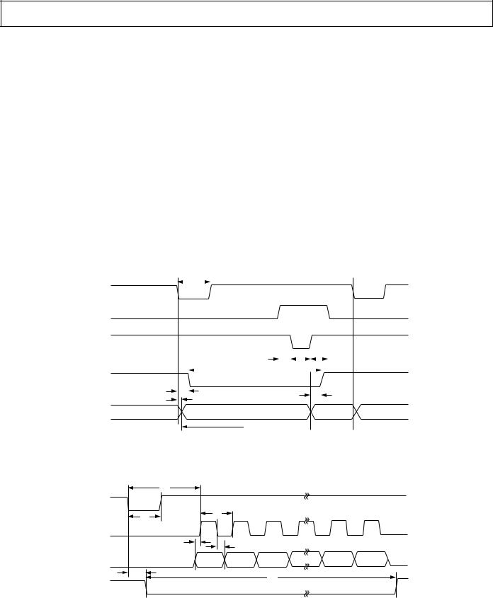
t6 
 t7
t7 
Figure 2. Basic Conversion Timing
|
t8 |
|
|
|
|
R/C |
|
|
|
|
|
|
t9 |
|
|
|
|
|
t1 |
|
|
|
|
DATACLK |
1 |
2 |
3 |
15 |
16 |
|
t10 |
t11 |
|
|
|
|
|
|
|
|
|
DATA |
MSB |
BIT 14 |
BIT 13 |
BIT 1 |
LSB |
VALID |
VALID |
VALID |
VALID |
VALID |
t2
t6
BUSY
Figure 3. Serial Data Timing for Reading Previous Conversion Results with Internal Clock (CS and EXT/ INT Set to Logic Low)
REV. A |
–7– |

AD974
can be read after the conversion is complete. The external clock can be either a continuous or discontinuous clock. A discontinuous clock can be either normally low or normally high when inactive. In the case of the discontinuous clock, the AD974 can be configured to either generate or not generate a SYNC output (with a continuous clock a SYNC output will always be produced).
Each of the methods will be described in the following sections and are illustrated in Figures 4 through 9. It should be noted that all timing diagrams assume that the receiving device is latching data on the rising edge of the external clock. If the falling edge of DATACLK is used then, in the case of a discontinuous clock, one less clock pulse is required than shown in Figures 4 through 7 to latch in a 16-bit word. Note that data is valid on the falling edge of a clock pulse (for t13 greater than t18) and the rising edge of the next clock pulse.
The AD974 provides error correction circuitry that can correct for an improper bit decision made during the first half of the conversion cycle. Normally the occurrence of an incorrect bit decision during a conversion cycle is irreversible. This error occurs as a result of noise during the time of the decision or due to insufficient settling time. As the AD974 is performing a conversion it is important that transitions not occur on digital input/output pins or degradation of the conversion result could occur. This is particularly important during the second half of the conversion process. For this reason it is recommended that when an external clock is being provided it be a discontinuous clock that is not toggling during the time that BUSY is low or,
more importantly, that it does not transition during the latter half of BUSY low.
EXTERNAL DISCONTINUOUS CLOCK DATA READ AFTER CONVERSION WITH NO SYNC OUTPUT GENERATED
Figure 4 illustrates the method by which data from conversion “n” can be read after the conversion is complete using a discontinuous external clock without the generation of a SYNC output. After a conversion is complete, indicated by BUSY returning high, the result of that conversion can be read while CS is Low and R/C is high. In this mode CS can be tied low. The MSB will be valid on the first falling edge and the second rising edge of DATACLK. The LSB will be valid on the 16th falling edge and the 17th rising edge of DATACLK. A minimum of 16 clock pulses are required for DATACLK if the receiving device will be latching data on the falling edge of DATACLK. A minimum of 17 clock pulses are required for DATACLK if the receiving device will be latching data on the rising edge of DATACLK.
The advantage of this method of reading data is that data is not being clocked out during a conversion and therefore conversion performance is not degraded.
When reading data after the conversion is complete, with the highest frequency permitted for DATACLK (15.15 MHz), the maximum possible throughput is approximately 195 kHz, and not the rated 200 kHz.
|
|
|
t12 |
|
|
|
|
|
|
|
t13 |
|
|
|
|
||
EXT |
|
|
t14 |
|
|
|
|
|
0 |
1 |
2 |
3 |
14 |
15 |
16 |
||
DATACLK |
||||||||
|
t1 |
|
|
|
|
|
|
|
R/C |
|
|
|
|
|
|
|
|
|
t2 |
|
|
|
|
|
|
|
BUSY |
|
|
|
|
|
|
|
|
|
t21 |
|
|
|
|
|
|
|
SYNC |
|
t18 |
|
|
|
|
t18 |
|
|
|
|
|
|
|
|||
DATA |
|
BIT 15 |
BIT 14 |
BIT 13 |
|
BIT 1 |
BIT 0 |
|
|
|
(MSB) |
|
|
|
|
(LSB) |
|
Figure 4. Conversion and Read Timing Using an External Discontinuous Data Clock (EXT/ INT Set to Logic High, CS Set to Logic Low)
–8– |
REV. A |

AD974
EXTERNAL DISCONTINUOUS CLOCK DATA READ DURING CONVERSION WITH NO SYNC OUTPUT GENERATED
Figure 5 illustrates the method by which data from conversion “n-1” can be read during conversion “n” while using a discontinuous external clock, without the generation of a SYNC output. After a conversion is initiated, indicated by BUSY going low, the result of the previous conversion can be read while CS is low and R/C is high. In this mode CS can be tied low. The MSB will be valid on the 1st falling edge and the 2nd rising edge of DATACLK. The LSB will be valid on the 16th falling edge and the 17th rising edge of DATACLK. A minimum of 16 clock pulses are required for DATACLK if the receiving device will be latching data on the falling edge of DATACLK. A minimum of 17 clock pulses are required for DATACLK if the receiving device will be latching data on the rising edge of DATACLK.
In this mode the data should be clocked out during the first half of BUSY so not to degrade conversion performance. This requires use of a 10 MHz DATACLK or greater, with data being read out as soon as the conversion process begins.
EXTERNAL DISCONTINUOUS CLOCK DATA READ AFTER CONVERSION WITH SYNC OUTPUT GENERATED
Figure 6 illustrates the method by which data from conversion “n” can be read after the conversion is complete using a
discontinuous external clock, with the generation of a SYNC output. What permits the generation of a SYNC output is a transition of DATACLK while either CS is high or while both CS and R/C are low. After a conversion is complete, indicated by BUSY returning high, the result of that conversion can be read while CS is Low and R/C is high. In this mode CS can be tied low. In Figure 6 clock pulse #0 is used to enable the generation of a SYNC pulse. The SYNC pulse is actually clocked out approximately 40 ns after the rising edge of clock pulse #1. The SYNC pulse will be valid on the falling edge of clock pulse #1 and the rising edge of clock pulse #2. The MSB will be valid on the falling edge of clock pulse #2 and the rising edge of clock pulse #3. The LSB will be valid on the falling edge of clock pulse #17 and the rising edge of clock pulse #18. The advantage of this method of reading data is that it is not being clocked out during a conversion and therefore conversion performance is not degraded.
When reading data after the conversion is complete, with the highest frequency permitted for DATACLK (15.15 MHz), the maximum possible throughput is approximately 195 kHz and not the rated 200 kHz.
|
t13 |
t12 |
|
|
|
|
|
t14 |
|
|
|
||
EXT |
0 |
1 |
2 |
15 |
16 |
|
DATACLK |
||||||
|
|
|
|
t22 |
||
|
t15 |
|
|
|
||
R/C |
|
|
|
|
|
|
|
t1 |
|
t20 |
|
|
|
|
|
|
|
|
||
BUSY |
|
|
|
|
|
|
t2 |
t21 |
|
|
|
|
|
SYNC |
t18 |
|
|
|
t18 |
|
|
|
|
|
|||
DATA |
|
BIT 15 |
BIT 14 |
|
BIT 0 |
|
|
(MSB) |
|
(LSB) |
|||
|
|
|
|
Figure 5. Conversion and Read Timing for Reading Previous Conversion Results During a Conversion Using External Discontinuous Data Clock (EXT/ INT Set to Logic High, CS Set to Logic Low)
|
|
|
t12 |
|
|
|
|
|
|
t13 |
|
t14 |
|
|
|
EXT |
|
|
|
|
|
|
|
DATACLK |
0 |
1 |
2 |
3 |
4 |
17 |
18 |
|
t15 |
t15 |
t15 |
|
|
|
|
R/C |
|
|
|
|
|
|
|
|
t2 |
|
|
|
|
|
|
BUSY |
|
t17 |
|
|
|
|
|
|
|
|
|
|
|
|
|
SYNC |
|
|
|
|
|
|
|
|
|
t12 |
|
|
|
t18 |
|
|
|
t18 |
|
|
|
||
DATA |
|
|
|
BIT 15 |
BIT 14 |
|
BIT 0 |
|
|
|
(MSB) |
|
(LSB) |
||
|
|
|
|
|
|
||
Figure 6. Conversion and Read Timing Using An External Discontinuous Data Clock (EXT/ INT Set to Logic High, CS Set to Logic Low)
REV. A |
–9– |

AD974
EXTERNAL DISCONTINUOUS CLOCK DATA READ DURING CONVERSION WITH SYNC OUTPUT GENERATED
Figure 7 illustrates the method by which data from conversion “n-1” can be read during conversion “n” while using a discontinuous external clock, with the generation of a SYNC output. What permits the generation of a SYNC output is a transition of DATACLK while either CS is High or while both CS and R/C are low. In Figure 7 a conversion is initiated by taking R/C low with CS tied low. While this condition exists a transition of
DATACLK, clock pulse #0, will enable the generation of a SYNC pulse. Less then 83 ns after R/C is taken low the BUSY
output will go low to indicate that the conversion process has
begun. Figure 7 shows R/C then going high and after a delay of greater than 15 ns (t15) clock pulse #1 can be taken high to request the SYNC output. The SYNC output will appear approximately 40 ns after this rising edge and will be valid on the falling edge of clock pulse #1 and the rising edge of clock pulse #2. The MSB will be valid approximately 40 ns after the rising edge of clock pulse #2 and can be latched off either the falling edge of clock pulse #2 or the rising edge of clock pulse #3. The LSB will be valid on the falling edge of clock pulse #17 and the rising edge of clock pulse #18.
Data should be clocked out during the first half of BUSY to avoid degrading conversion performance. This requires use of a 10 MHz DATACLK or greater, with data being read out as soon as the conversion process begins.
|
|
|
t12 |
|
|
|
|
|
|
t13 |
|
t14 |
|
|
|
EXT |
|
|
|
|
|
|
|
DATACLK |
0 |
1 |
2 |
3 |
4 |
17 |
18 |
t15 |
|
t15 |
|
|
|
|
t22 |
R/C |
|
|
|
|
|
|
|
|
|
t1 |
|
|
t20 |
|
|
|
|
|
|
|
|
|
|
BUSY |
|
|
|
|
|
|
|
|
t2 |
t17 |
|
|
|
|
|
|
|
|
|
|
|
|
|
SYNC |
|
|
t12 |
|
|
|
|
|
|
|
|
|
|
|
|
|
|
|
|
t18 |
|
|
t18 |
DATA |
|
|
|
BIT 15 |
BIT 14 |
|
BIT 0 |
|
|
|
(MSB) |
|
(LSB) |
||
|
|
|
|
|
|
Figure 7. Conversion and Read Timing for Reading Previous Conversion Results During a Conversion Using External Discontinuous Data Clock (EXT/ INT Set to Logic High, CS Set to Logic Low)
–10– |
REV. A |