

CIRCUIT INFORMATION
The AD7912/AD7922 are fast, 2-channel, 10-/12-bit, single supply, analog-to-digital converters (ADCs), respectively. The parts can be operated from a 2.35 V to 5.25 V supply. When operated from either a 5 V supply or a 3 V supply, the
AD7912/AD7922 are capable of throughput rates of 1 MSPS when provided with an 18 MHz clock.
The AD7912/AD7922 provide the user with an on-chip track- and-hold, an ADC, and a serial interface, all housed in a tiny
8-lead TSOT package or 8-lead MSOP package, which offer the user considerable space-saving advantages over alternative solutions. The serial clock input accesses data from the parts, controls the transfer of data written to the ADC, and provides the clock source for the successive approximation ADC. The analog input range is 0 to VDD. An external reference is not required for the ADC, and neither is there a reference on-chip. The reference for the AD7912/AD7922 is derived from the power supply and, therefore, gives the widest dynamic input range.
The AD7912/AD7922 feature a power-down option that allows power saving between conversions. The power-down feature is implemented across the standard serial interface as described in the Modes of Operation section. The AD7912/AD7922 can also be used in daisy-chain mode when several AD7912/AD7922 are connected in a daisy chain. This mode of operation is selected by controlling the logic state of the CS signal. The fourth MSB on the DOUT pin indicates if the ADC is in normal mode or daisy-chain mode.
CONVERTER OPERATION
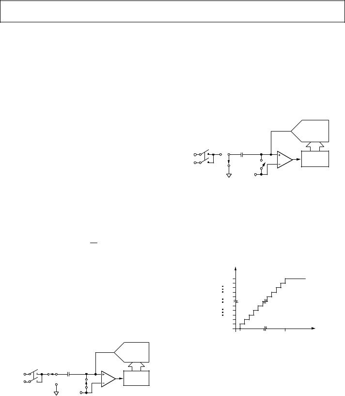
The AD7912/AD7922 are 10-/12-bit successive approximation ADCs based around a charge redistribution DAC. Figure 19 and Figure 20 show simplified schematics of the ADC. Figure 19 shows the ADC during its acquisition phase. SW2 is closed and SW1 is in Position A, the comparator is held in a balanced condition, and the sampling capacitor acquires the signal on the selected VIN channel.
|
|
|
|
CHARGE |
|
|
|
REDISTRIBUTION |
|
|
|
|
|
DAC |
|
A |
SAMPLING |
|
|
VIN0 |
CAPACITOR |
|
|
|
|
|
|
CONTROL |
|
VIN1 |
SW1 |
ACQUISITION |
SW2 |
LOGIC |
|
B |
PHASE |
|
-0-016 |
|
|
VDD/2 |
COMPARATOR |
|
|
AGND |
|
04351 |
|
Figure 19. ADC Acquisition Phase
AD7912/AD7922
When the ADC starts a conversion (see Figure 20), SW2 opens and SW1 moves to Position B, causing the comparator to become unbalanced. The control logic and the charge redistribution DAC are used to add and subtract fixed amounts of charge from the sampling capacitor to bring the comparator back into a balanced condition. When the comparator is rebalanced, the conversion is complete. The control logic generates the ADC output code. Figure 21 shows the ADC transfer function.
|
|
|
|
CHARGE |
|
|
|
|
REDISTRIBUTION |
|
|
|
|
DAC |
|
A |
SAMPLING |
|
|
VIN0 |
CAPACITOR |
|
|
|
|
|
|
CONTROL |
|
VIN1 |
SW1 |
CONVERSION |
SW2 |
LOGIC |
|
B |
PHASE |
|
04351-0-017 |
|
AGND |
|
||
|
|
VDD/2 |
COMPARATOR |
|
Figure 20. ADC Conversion Phase
ADC TRANSFER FUNCTION
The output coding of the AD7912/AD7922 is straight binary. The designed code transitions occur at the successive integer LSB values, that is, 1 LSB, 2 LSBs, and so on. The LSB size is VDD/4096 for the AD7922 and VDD/1024 for the AD7912. The ideal transfer characteristic for the AD7912/AD7922 is shown in Figure 21.
|
111...111 |
|
|
|
111...110 |
|
|
CODE |
111...000 |
|
|
|
|
||
ADC |
011...111 |
|
|
1LSB = VREF/4096 (AD7922) |
|||
|
|||
|
1LSB = VREF/1024 (AD7912) |
||
|
000...010 |
|
|
|
000...001 |
|
|
|
000...000 |
|
|
|
0V 1LSB |
+VDD – 1LSB |
|
|
ANALOG INPUT |
04351018-0- |
|
Figure 21. AD7912/AD7922 Transfer Characteristic
Rev. 0 | Page 15 of 32
AD7912/AD7922
TYPICAL CONNECTION DIAGRAM
Figure 22 shows a typical connection diagram for the AD7912/ AD7922. VREF is taken internally from VDD and as such VDD should be well decoupled. This provides an analog input range of 0 V to VDD. The conversion result is output in a 16-bit word with two leading zeros, followed by the channel identifier bit that identifies the channel converted, followed by the mode bit that indicates the current mode of operation, and by the MSB of the 12-bit or 10-bit result. For the AD7912, the 10-bit result is followed by two trailing zeros. See the Serial Interface section.
Alternatively, because the supply current required by the AD7912/AD7922 is so low, a precision reference can be used as the supply source to the AD7912/AD7922. A REF19x voltage reference (REF195 for 5 V or REF193 for 3 V) can be used to supply the required voltage to the ADC (see Figure 22). This configuration is especially useful, if the power supply is quite noisy or if the system supply voltages are at some value other than 5 V or 3 V (for example, 15 V). The REF19x outputs a steady voltage to the AD7912/AD7922. If the low dropout REF193 is used, the current it needs to supply to the AD7912/ AD7922 is typically1.5 mA. When the ADC is converting at a rate of 1 MSPS, the REF193 needs to supply a maximum of
2 mA to the AD7912/AD7922. The load regulation of the REF193 is typically 10 ppm/mA (REF193, VS = 5 V), which results in an error of 20 ppm (60 µV) for the 2 mA drawn from it. This corresponds to a 0.082 LSB error for the AD7922 with VDD = 3 V from the REF193 and a 0.061 LSB error for the AD7912.
For applications where power consumption is a concern, the power-down mode of the ADC and the sleep mode of the REF19x reference should be used to improve power performance. See the Modes of Operation section.
|
|
|
3V |
REF193 |
5V |
|
|
|
|
1µF |
SUPPLY |
||
1.5mA |
|
|
|
|||
0.1µF |
10µF |
0.1µF |
||||
|
TANT |
|||||
|
|
|
|
|
||
680nF |
|
|
|
|
|
|
|
VDD |
|
|
|
|
|
0V TO VDD |
VIN0 |
AD7912/ |
SCLK |
|
||
INPUT |
|
CS |
|
|||
|
VIN1 AD7922 |
µC/µP |
||||
|
DIN |
|||||
|
|
|
|
019-0-04351 |
||
|
GND |
|
DOUT |
|||
|
|
|
||||
|
|
|
|
|
||
|
|
|
|
SERIAL |
|
|
|
|
|
|
INTERFACE |
|
|
Figure 22. REF193 as Power Supply to AD7912/AD7922
Table 6 provides some typical performance data with various references used as a VDD source and a 50 kHz input tone under the same setup conditions.
Table 6. AD7922 Performance for Various Voltage References IC
Reference Tied to VDD |
AD7922 SNR Performance (dB) |
|
|
AD780 at 3 V |
−73 |
REF193 |
−72.42 |
ADR433 |
−72.9 |
AD780 at 2.5 V |
−72.86 |
REF192 |
−72.27 |
ADR421 |
−72.75 |
|
|
ANALOG INPUT
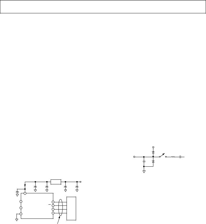
Figure 23 shows an equivalent circuit of the analog input structure of the AD7912/AD7922. The two diodes, D1 and D2, provide ESD protection for the analog input. Care must be taken to ensure that the analog input signal never exceeds the supply rails by more than 300 mV, because this would cause these diodes to become forward biased and start conducting current into the substrate. The maximum current these diodes can conduct without causing irreversible damage to the part is 10 mA.
VDD
|
D1 |
|
C2 |
|
R1 |
20pF |
|
VIN |
|
||
|
|
||
|
|
|
|
C1 |
D2 |
|
|
6pF |
|
|
04351-0-020
Figure 23. Equivalent Analog Input Circuit
The capacitor C1 in Figure 23 is typically about 6 pF and can primarily be attributed to pin capacitance. The resistor R1 is a lumped component made up of the on resistance of the track-and-hold switch and also includes the on resistance of the input multiplexer. This resistor is typically about 100 Ω. The capacitor C2 is the ADC sampling capacitor and has a capacitance of 20 pF typically.
For ac applications, removing high frequency components from the analog input signal is recommended using a band-pass filter on the relevant analog input pin. In applications where harmonic distortion and signal-to-noise ratio are critical, the analog input should be driven from a low impedance source. Large source impedances can significantly affect the ac performance of the ADC. This might necessitate the use of an input buffer amplifier. The choice of the op amp is a function of the particular application.
Rev. 0 | Page 16 of 32

Table 7 provides some typical performance data with various op amps used as the input buffer, and a 50 kHz input tone under the same setup conditions.
Table 7. AD7922 Performance for Various Input Buffers
Op Amp in the Input |
AD7922 SNR Performance (dB) |
Buffer |
50 kHz Input , VDD = 3.6 V |
|
|
Single op amps |
|
AD8038 |
−72.79 |
AD8510 |
−72.35 |
AD8021 |
−72.2 |
Dual op amps |
|
AD712 |
−72.68 |
AD8022 |
−72.88 |
|
|
When no amplifier is used to drive the analog input, the source impedance should be limited to low values. The maximum source impedance depends on the amount of total harmonic distortion (THD) that can be tolerated. The THD increases as the source impedance increases and performance degrades (see Figure 16).
DIGITAL INPUTS
The digital inputs applied to the AD7912/AD7922 are not limited by the maximum ratings that limit the analog input. Instead, the digital inputs applied can go to 7 V and are not restricted by the VDD + 0.3 V limit as on the analog input. For example, if the AD7912/AD7922 are operated with a VDD of 3 V, then 5 V logic levels could be used on the digital inputs. However, it is important to note that the data output on DOUT still has 3 V logic levels when VDD = 3 V. Another advantage of
SCLK, DIN, and CS not being restricted by the VDD + 0.3 V limit
is that power supply sequencing issues are avoided. If CS, DIN, or SCLK are applied before VDD, then there is no risk of latch-up as there would be on the analog inputs if a signal greater than 0.3 V were applied prior to VDD.
DIN INPUT
The channel to be converted on in the next conversion is selected by writing to the DIN pin. Data on the DIN pin is loaded into the AD7912/AD7922 on the falling edge of SCLK. The data is transferred into the part on the DIN pin at the same time that the conversion result is read from the part. Only the third and fourth bits of the DIN word are used; the rest are ignored by the ADC.
The third MSB is the channel identifier bit, which identifies the channel to be converted on in the next conversion,
VIN0 (CHN = 0) or VIN1 (CHN = 1).
AD7912/AD7922
The fourth MSB, STY, is related to the mode of operation of the device. To keep the AD7912/ AD7922 in daisy-chain mode, the CHN and STY bits have to be inverted during the conversions (STY ≠ CHN). A conversion with STY = CHN on the input forces the device to normal mode in the next cycle. See the
Daisy-Chain Mode section for more details.
If the AD7912/AD7922 are not going to be used in daisy-chain mode, it is recommended to keep STY and CHN the same (STY = CHN). In that case, the channel can be selected by tying DIN either high or low during a conversion cycle.
To summarize:
CHN = 0, Channel 0 selected for next conversion.
CHN = 1, Channel 1 selected for next conversion.
CHN = STY, forces normal mode in the next cycle.
CHN ≠ STY, keeps the AD7912/AD7922 in daisy-chain mode.
MSB |
|
|
|
|
04351-0-021 |
|
|
|
|
|
LSB |
||
X |
X |
CHN |
STY |
DON'T CARE |
|
|
|
|
|
|
|
|
|
Figure 24. AD7912/AD7922 DIN Word
DOUT OUTPUT
The conversion result from the AD7912/AD7922 is provided on this output as a serial data stream. The bits are clocked out on the SCLK falling edge at the same time that the conversion is taking place.
The serial data stream for the AD7922 consists of two leading zeros followed by the bit that identifies the channel converted, the bit that indicates the current mode of operation, and the 12-bit conversion result with MSB provided first.
For the AD7912, the serial data stream consists of two leading zeros followed by the bit that identifies the channel converted, the bit that indicates the current mode of operation, and the 10-bit conversion result with MSB provided first, followed by two trailing zeros.
The CHN and MOD bits on DOUT indicate to the user the current mode of operation of the ADC. If CHN = MOD, the AD7912/AD7922 are in normal mode. Otherwise, if
CHN ≠ MOD, the AD7912/AD7922 are in daisy-chain mode.
MSB |
|
|
|
|
|
LSB |
|
|
0 |
0 |
CHN |
MOD |
CONVERSION RESULT |
0 |
0 |
AD7912 |
04351-0-022 |
|
|
|
|
|
|
|
AD7922 |
|
|
|
|
|
|
|
|
||
0 |
0 |
CHN |
MOD |
CONVERSION RESULT |
|
|||
|
|
|||||||
|
|
|
|
|
|
|
|
|
Figure 25. AD7912/AD7922 DOUT Word
Rev. 0 | Page 17 of 32