

AD7912/AD7922
TIMING SPECIFICATIONS
Guaranteed by characterization.
All input signals are specified with tr = tf = 5 ns (10% to 90% of VDD) and timed from a voltage level of 1.6 V. VDD = 2.35 V to 5.25 V; TA = TMIN to TMAX, unless otherwise noted.
Table 3.
|
Parameter |
Limit at TMIN, |
Unit |
|
Description |
||||||
|
|
TMAX |
|
|
|
|
|
|
|
|
|
|
fSCLK1 |
10 |
kHz min2 |
|
|
|
|
|
|
|
|
|
|
18 |
MHz max |
|
|
|
|
|
|
|
|
|
tCONVERT |
16 × tSCLK |
|
|
|
AD7922 |
|||||
|
|
14 × tSCLK |
|
|
|
AD7912 |
|||||
|
tQUIET |
30 |
ns min |
|
Minimum quiet time required between bus relinquish and start of next conversion |
||||||
|
t1 |
15 |
ns min |
|
|
|
|
|
|||
|
|
Minimum |
CS |
pulse width |
|||||||
|
t2 |
10 |
ns min |
|
|
|
|
||||
|
|
CS |
to SCLK setup time |
||||||||
|
t33 |
30 |
ns max |
|
|
||||||
|
|
Delay from |
CS |
until DOUT three-state is disabled |
|||||||
|
t43 |
45 |
ns max |
|
DOUT access time after SCLK falling edge |
||||||
|
t5 |
0.4 tSCLK |
ns min |
|
SCLK low pulse width |
||||||
|
t6 |
0.4 tSCLK |
ns min |
|
SCLK high pulse width |
||||||
|
t74 |
10 |
ns min |
|
SCLK to DOUT valid hold time |
||||||
|
t8 |
5 |
ns min |
|
DIN setup time prior to SCLK falling edge |
||||||
|
t9 |
6 |
ns min |
|
DIN hold time after SCLK falling edge |
||||||
|
t105 |
30 |
ns max |
|
SCLK falling edge to DOUT three-state |
||||||
|
|
10 |
ns min |
|
SCLK falling edge to DOUT three-state |
||||||
|
tPOWER-UP6 |
1 |
µs max |
|
Power-up time from full power-down |
||||||
|
|
|
|
|
|
|
|
|
|
|
|
1 Mark/space ratio for SCLK input is 40/60 to 60/40.
2 Minimum fSCLK at which specifications are guaranteed.
3 Measured with the load circuit in Figure 2 and defined as the time required for the output to cross VIH or VIL voltage. 4 Measured with a 50 pF load capacitor.
5T10 is derived from the measured time taken by the data outputs to change 0.5 V when loaded with the circuit in Figure 2. The measured number is then extrapolated back to remove the effects of charging or discharging the 50 pF capacitor. This means that the time, t10, quoted in the timing characteristics is the true bus relinquish
time of the part and is independent of the bus loading. 6 See the Power-Up Time section.
TIMING DIAGRAMS
|
200µA |
IOL |
|
TO OUTPUT |
|
|
1.6V |
PIN |
CL |
|
|
|
|
||
|
|
|
|
|
50pF |
|
04351-0-002 |
|
200µA |
IOH |
|
|
|
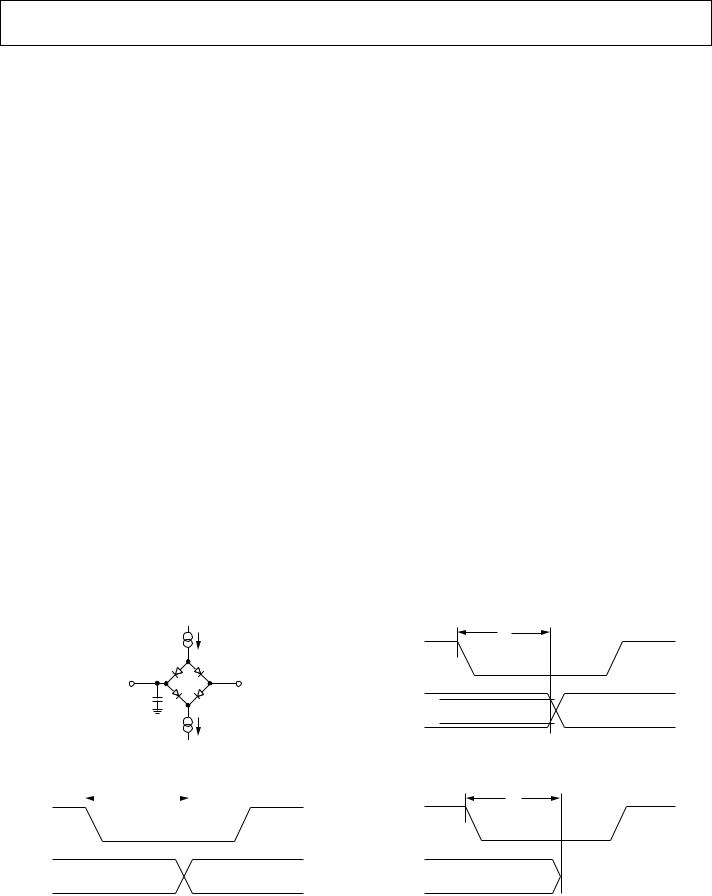
Figure 2. Load Circuit for Digital Output Timing Specifications
SCLK |
|
|
|
t4 |
|
|
|
|
-043510-003 |
||
|
|
||||||||||
|
|
|
|
|
|
|
|
||||
|
|
|
|
|
|
|
|
||||
|
|
|
VIH |
||||||||
|
|
|
|
|
|
|
|
|
|
||
DOUT |
|
|
|||||||||
|
|
VIL |
|||||||||
|
|
|
|||||||||
|
|
|
|
|
|
|
|
|
|
|
|
|
|
|
|
|
|
|
|
|
|
|
|
Figure 3. Access Time after SCLK Falling Edge
|
t7 |
SCLK |
|
VIH |
04351-0-004 |
VIL |
|
DOUT |
|
Figure 4. Hold Time after SCLK Falling Edge
t10
SCLK
|
04351-0-005 |
DOUT |
1.6V |
|
Figure 5. SCLK Falling Edge to DOUT Three-State
Rev. 0 | Page 7 of 32