- •FEATURES
- •APPLICATIONS
- •FUNCTIONAL BLOCK DIAGRAM
- •GENERAL DESCRIPTION
- •PRODUCT HIGHLIGHTS
- •SPECIFICATIONS
- •AD7912 SPECIFICATIONS
- •AD7922 SPECIFICATIONS
- •TIMING SPECIFICATIONS
- •TIMING DIAGRAMS
- •TIMING EXAMPLES
- •Timing Example 1
- •Timing Example 2
- •ABSOLUTE MAXIMUM RATINGS
- •ESD CAUTION
- •PIN CONFIGURATIONS AND FUNCTION DESCRIPTIONS
- •TERMINOLOGY
- •TYPICAL PERFORMANCE CHARACTERISTICS
- •CIRCUIT INFORMATION
- •CONVERTER OPERATION
- •ADC TRANSFER FUNCTION
- •TYPICAL CONNECTION DIAGRAM
- •ANALOG INPUT
- •DIGITAL INPUTS
- •DIN INPUT
- •DOUT OUTPUT
- •MODES OF OPERATION
- •NORMAL MODE
- •POWER-DOWN MODE
- •POWER-UP TIME
- •DAISY-CHAIN MODE
- •DAISY-CHAIN EXAMPLE
- •POWER VS. THROUGHPUT RATE
- •SERIAL INTERFACE
- •MICROPROCESSOR INTERFACING
- •AD7912/AD7922 to TMS320C541 Interface
- •AD7912/AD7922 to ADSP-218x
- •AD7912/AD7922 to DSP563xx Interface
- •APPLICATION HINTS
- •GROUNDING AND LAYOUT
- •EVALUATING AD7912/AD7922 PERFORMANCE
- •OUTLINE DIMENSIONS
- •ORDERING GUIDE

2-Channel, 2.35 V to 5.25 V,
1 MSPS, 10-/12-Bit ADCs
AD7912/AD7922
FEATURES
Fast throughput rate: 1 MSPS Specified for VDD of 2.35 V to 5.25 V Low power:
4.8 mW typ at 1 MSPS with 3 V supplies 15.5mW typ at 1 MSPS with 5 V supplies
Wide input bandwidth:
71 dB minimum SNR at 100 kHz input frequency Flexible power/serial clock speed management No pipeline delays
High speed serial interface: SPI®/QSPI™/MICROWIRE™/DSP compatible
Standby mode: 1 µA maximum Daisy-chain mode
8-lead TSOT package
8-lead MSOP package
APPLICATIONS
Battery-powered systems:
Personal digital assistants
Medical instruments
Mobile communications
Instrumentation and control systems
Data acquisition systems
High speed modems
Optical sensors
GENERAL DESCRIPTION
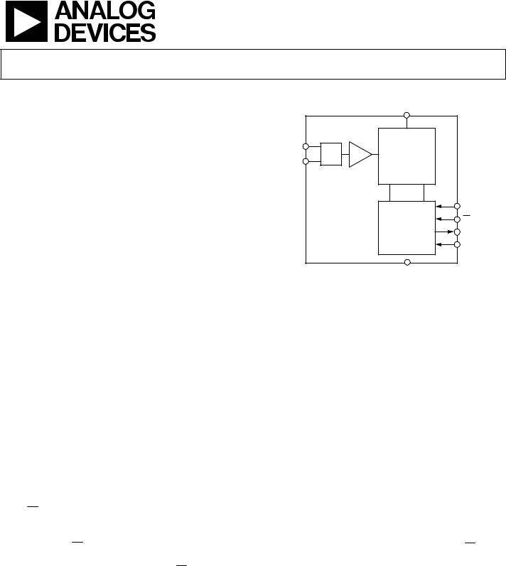
The AD7912/AD79221 are 10-bit and 12-bit, high speed, low power, 2-channel successive approximation ADCs, respectively. The parts operate from a single 2.35 V to 5.25 V power supply and feature throughput rates of up to 1 MSPS. The parts contain a low noise, wide bandwidth track-and-hold amplifier, which can handle input frequencies in excess of 6 MHz.
The conversion process and data acquisition are controlled using CS and the serial clock, allowing the devices to interface with microprocessors or DSPs. The conversion rate is determined by the SCLK signal. The input signal is sampled on the falling edge of CS and the conversion is also initiated at this point. The channel to be converted is selected through the DIN pin, and the mode of operation is controlled by CS. The serial data stream from the DOUT pin has a channel identifier bit and mode identifier bit, which provide information about the converted channel and the current mode of operation.
Rev. 0
Information furnished by Analog Devices is believed to be accurate and reliable. However, no responsibility is assumed by Analog Devices for its use, nor for any infringements of patents or other rights of third parties that may result from its use. Specifications subject to change without notice. No license is granted by implication or otherwise under any patent or patent rights of Analog Devices. Trademarks and registered trademarks are the property of their respective owners.
FUNCTIONAL BLOCK DIAGRAM
VDD
VIN0 |
|
10-/12-BIT |
|
MUX |
T/H |
SUCCESSIVE |
|
VIN1 |
|
APPROXIMATION |
|
|
|
ADC |
|
|
|
|
SCLK |
AD7912/AD7922 |
|
CS |
|
CONTROL LOGIC |
DOUT |
||
|
|
|
|
|
|
|
DIN |
|
|
|
04351-0001- |
|
|
GND |
|
Figure 1.
Several AD7912/AD7922 can be connected together in a daisy chain. The AD7912/AD7922 feature a daisy-chain mode that allows the user to read the conversion results from the ADCs contained in the chain. The AD7912/AD7922 use advanced design techniques to achieve very low power dissipation at high throughput rates. The reference for the part is taken internally from VDD, thereby allowing the widest dynamic input range to the ADC.
PRODUCT HIGHLIGHTS
1.2-channel, 1 MSPS, 10-/12-bit ADCs in TSOT package.
2.High throughput with low power consumption.
3.Flexible power/serial clock speed management.
The conversion rate is determined by the serial clock. The parts also feature a power-down mode to maximize power efficiency at lower throughput rates. Average power consumption is reduced when the power-down mode is used while not converting. Current consumption is 1 µA maximum and 50 nA typically when in power-down mode.
4.Daisy-chain mode.
5.No pipeline delay.
The parts feature a standard successive approximation ADC with accurate control of the sampling instant via a CS input and once-off conversion control.
1 Protected by U.S. Patent Number 6,681,332.
One Technology Way, P.O. Box 9106, Norwood, MA 02062-9106, U.S.A. Tel: 781.329.4700 www.analog.com Fax: 781.326.8703 © 2004 Analog Devices, Inc. All rights reserved.

AD7912/AD7922
TABLE OF CONTENTS |
|
Specifications..................................................................................... |
3 |
AD7912 Specifications................................................................. |
3 |
AD7922 Specifications................................................................. |
5 |
Timing Specifications .................................................................. |
7 |
Timing Diagrams.......................................................................... |
7 |
Timing Examples.......................................................................... |
8 |
Absolute Maximum Ratings............................................................ |
9 |
ESD Caution.................................................................................. |
9 |
Pin Configurations and Function Descriptions ......................... |
10 |
Terminology .................................................................................... |
11 |
Typical Performance Characteristics ........................................... |
13 |
Circuit Information........................................................................ |
15 |
Converter Operation.................................................................. |
15 |
ADC Transfer Function............................................................. |
15 |
Typical Connection Diagram ................................................... |
16 |
Analog Input ............................................................................... |
16 |
Digital Inputs .............................................................................. |
17 |
REVISION HISTORY |
|
Revision 0: Initial Version |
|
DIN Input.................................................................................... |
17 |
DOUT Output ............................................................................ |
17 |
Modes of Operation ....................................................................... |
18 |
Normal Mode.............................................................................. |
18 |
Power-Down Mode.................................................................... |
18 |
Power-Up Time .......................................................................... |
20 |
Daisy-Chain Mode..................................................................... |
20 |
Daisy-Chain Example................................................................ |
22 |
Power vs. Throughput Rate ........................................................... |
24 |
Serial Interface ................................................................................ |
25 |
Microprocessor Interfacing....................................................... |
26 |
Application Hints ........................................................................... |
28 |
Grounding and Layout .............................................................. |
28 |
Evaluating AD7912/AD7922 Performance................................. |
29 |
Outline Dimensions ....................................................................... |
30 |
Ordering Guide .......................................................................... |
30 |
Rev. 0 | Page 2 of 32
