

ЦОС_Заочники2013 / Книги по ЦОС / Дополнительная литература / Основы ЦОС (на англ.яз) / MS4
.pdfDACS FOR DSP APPLICATIONS
SECTION 4
DACs FOR DSP APPLICATIONS
■DAC Structures
■Low Distortion DAC Architectures
■DAC Logic
■Sigma-Delta DACs
■Direct Digital Synthesis (DDS)
4.a
DACS FOR DSP APPLICATIONS
4.b

DACS FOR DSP APPLICATIONS
SECTION 4
DACs FOR DSP APPLICATIONS
Walt Kester, James Bryant
DAC STRUCTURES
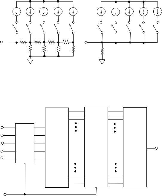
The most commonly used DAC structures (other than a simple 1-bit DAC based on a single switch used with a reference voltage) are binary weighted DACs or ladder networks, but these, though relatively simple in structure, require quite complex analysis. We will start by examining one of the simplest structures of all, the Kelvin divider shown in Figure 4.1. An N-bit version of this DAC simply consists of 2N equal resistors in series. The output is taken from the appropriate tap by closing one of the 2N switches by decoding 1 of 2N switches from the N-bit data. Recent DACs using this architecture are referred to as “string DACs.”
SIMPLEST VOLTAGE OUTPUT DAC: THE KELVIN DIVIDER
(“STRING DAC”)
VREF
8 FROM 3 |
3-BIT |
DECODER |
DIGITAL |
|
INPUT |
ANALOG
OUTPUT
Figure 4.1
This architecture is simple, has a voltage output (but a code-varying ZOUT), and is inherently monotonic (even if a resistor is zero, OUTPUTN cannot exceed OUTPUTN+1). It is linear if all the resistors are equal, but may be made deliberately non-linear if a non-linear DAC is required. Since only two switches operate during a transition, it is a low-glitch architecture. Its major drawback is the
4.1

DACS FOR DSP APPLICATIONS
large number of resistors required for high resolution, and as a result it is not commonly used - but, as we shall see later, it is used as a component in more complex DAC structures.
There is an analogous current output DAC which consists, again, of 2N resistors (or current sources), but in this case they are all connected in parallel between the reference voltage input and the virtual ground output (see Figure 4.2).
THE SIMPLEST CURRENT OUTPUT DAC
VREF |
|
7 FROM 3 |
CURRENT |
DECODER |
|
|
OUTPUT INTO |
|
VIRTUAL |
|
GROUND |
|
(USUALLY AN |
|
OP-AMP I-V |
|
CONVERTER) |
3-BIT
DIGITAL INPUT
Figure 4.2
In this DAC, once a resistor is switched into circuit by increasing digital code, any further increases do not switch it out again. The structure is thus inherently monotonic, irrespective of inaccuracies in the resistors, and like the previous case, may be made intentionally non-linear where a specific non-linearity is required. Again, as in the previous case, the architecture is rarely, if ever, used to fabricate a complete DAC because of the large numbers of resistors and switches required. However, it is often used as a component in a more complex DAC structure.
Unlike the Kelvin divider, this type of DAC does not have a unique name, although both types are referred to as fully decoded DACs or thermometer DACs or string DACs.
Fully-decoded DACs are often used as components of more complex DACs. The most common are "segmented DACs" where part of the output of a fully decoded DAC is further subdivided. The structure is used because the fully decoded DAC is inherently monotonic, so if the subdivision is also monotonic, the whole resulting DAC is also monotonic.
4.2

DACS FOR DSP APPLICATIONS
A voltage segmented DAC (see Figure 4.3) works by further sub-dividing the voltage across one resistor of a Kelvin divider. The sub-division may be done with a further Kelvin divider (in which case the whole structure is known as a "Kelvin-Varley divider", or with some other DAC structure.
|
SEGMENTED VOLTAGE DACs |
|
|
|
KELVIN-VARLEY DIVIDER |
KELVIN DIVIDER AND |
|
|
(“STRING DAC”) |
|
|
|
R-2R LADDER NETWORK |
|
|
VREF |
|
VREF |
OUTPUT |
|
|
|
|
OUTPUT
NOTE:
MSB OF LADDER
ON RIGHT
IF THE LADDER NETWORK
IS MONOTONIC, THE
WHOLE DAC IS
MONOTONIC
Figure 4.3
In all DACs, the output is the product of the reference voltage and the digital code, so in that sense, all DACs are multiplying DACs, but many DACs operate well only over a limited range of Vref. True MDACs, however, are designed to operate over a wide range of Vref. A strict definition of a multiplying DAC demands that its reference voltage range includes 0V, and many, especially current mode ladder networks with CMOS switches, permit positive, negative, and AC Vref. DACs which do not work down to 0V Vref are still useful, however, and types where Vref can vary by 10:1 or so are often called MDACs, although a more accurate description might be "semi-multiplying" DACs.
LOW DISTORTION DAC ARCHITECTURES
Because of the emphasis in communications systems on DDS DACs with high SFDR, much effort has been placed on determining optimum DAC architectures. Practically all low distortion high speed DACs make use of some form of nonsaturating current-mode switching. A straight binary DAC with one current switch per bit produces code-dependent glitches as discussed above and is certainly not the most optimum architecture (Figure 4.4). A DAC with one current source per code level can be shown not to have code-dependent glitches, but it is not practical to implement for high resolutions. However, this performance can be approached by
4.3
DACS FOR DSP APPLICATIONS
decoding the first few MSBs into a "thermometer" code and have one current switch per level. For example, a 5-bit thermometer DAC would have an architecture similar to that shown in Figure 4.5.
5-BIT BINARY DAC ARCHITECTURES
I |
I |
I |
I |
I |
I |
I/2 |
I/4 |
I/8 |
I/16 |
MSB |
|
|
|
|
MSB |
R |
R |
R |
R |
|
|
OUTPUT |
2R |
2R |
2R |
R |
OUTPUT |
|
R (CAN BE EXTERNAL) |
Figure 4.4
5-BIT “THERMOMETER” OR “FULLY-DECODED” DAC MINIMIZES CODE-DEPENDENT GLITCHES
MSB |
|
|
|
|
|
|
5-BIT |
|
|
31-BIT |
|
31 |
|
LATCH |
5-TO-31 |
|
|
CURRENT |
||
|
DECODE |
31 |
LATCH |
31 |
EQUAL |
|
|
OUTPUT |
|||||
|
LOGIC |
LINES |
|
LINES CURRENT |
||
LSB |
|
|
|
|
SWITCHES |
|
|
|
|
|
|
|
|
CLOCK
Figure 4.5
4.4

DACS FOR DSP APPLICATIONS
The input binary word is latched and then decoded into 31 outputs which drive a second latch. The output of the second latch drives 31 equally weighted current switches whose outputs are summed together. This scheme effectively removes nearly all the code-dependence of the output glitch. The residual glitch that does occur at the output is equal regardless of the output code change (it is codeindependent) and can be filtered because it occurs at the DAC update frequency and its harmonics. The distortion mechanisms associated with the full-decoded architecture are primarily asymmetrical output slewing, finite switch turn-on and turn-off times, and integral nonlinearity.
The obvious disadvantage of this type of thermometer DAC is the large number of latches and switches required to make a 14, 12, 10, or even 8-bit DAC. However, if this technique is used on the 5 MSBs of an 8, 10, 12, or 14-bit DAC, a significant reduction in the code-dependent glitch is possible. This process is called segmentation and is quite common in low distortion DACs.
Figure 4.6 shows a scheme whereby the first 5 bits of a 10-bit DAC are decoded as described above and drive 31 equally weighted switches. The last 5 bits are derived from binarily weighted current sources. Equally weighted current sources driving an R/2R resistor ladder could be used to derive the LSBs, however, this approach requires thin film resistors which are not generally available on a low-cost CMOS process. Also, the use of R/2R networks lowers the DAC output impedance, thereby requiring more drive current to develop the same voltage across a fixed load resistance.
10-BIT SEGMENTED DAC
|
|
|
5 |
|
31 |
|
31 |
|
FULLY |
|
|
|
|
|
|
|
MSB |
|
|
|
|
|
|
|
|
|
|
|
|
|
|
|
DECODED |
|
|
|
||
|
|
|
|
DECODE |
|
|
|
|
|
|
||
|
|
|
|
|
|
|
|
MSB |
|
|
|
|
|
|
|
|
|
|
|
|
|
|
|
|
|
10 |
10-BIT |
|
|
|
36-BIT |
|
|
DAC |
|
|
|
|
|
LATCH |
|
|
|
LATCH |
|
|
|
CURRENT |
|||
|
|
|
|
|
|
|
|
|
|
|
OUTPUT |
|
|
|
|
|
|
|
|
|
|
|
|
|
|
|
|
|
|
|
|
|
|
|
|
|
|
|
|
|
|
5 |
|
|
5 |
|
BINARY |
|
|
|
|
|
|
|
|
|
|
LSB |
|
|
|
|||
|
|
|
|
|
|
|
|
|
DAC |
|
|
|
CLOCK |
|
|
|
|
|
|
|
|
|
|
|
|
|
|
|
|
|
|
|
|
|
|
|
|
|
|
|
|
|
|
|
|
|
|
|
|
|
|
|
|
|
|
|
|
|
|
|
|
|
|
|
Figure 4.6
4.5
DACS FOR DSP APPLICATIONS
The AD9772 14-bit, 150MSPS TxDAC™ uses three sections of segmentation as shown in Figure 4.7. Other members of the AD977x-family and the AD985x-family also use this same core.
The first 5 bits (MSBs) are fully decoded and drive 31 equally weighted current switches, each supplying 512 LSBs of current. The next 4 bits are decoded into 15 lines which drive 15 current switches, each supplying 32 LSBs of current. The 5 LSBs are latched and drive a traditional binary weighted DAC which supplies 1 LSB per output level. A total of 51 current switches and latches are required to implement this architecture.
AD9772 TxDAC™ 14-BIT CMOS DAC CORE
|
|
5 |
|
31 |
|
31 |
|
|
|
BITS 1-5 |
|
|
|
|
|
|
DECODE |
|
|
|
14 |
14-BIT |
|
5-TO-31 |
|
51-BIT |
|
|
|
|
|
|||
|
LATCH |
4 |
|
|
|
|
|
|
15 |
LATCH |
15 |
||
|
|
|||||
|
|
|
||||
|
|
BITS 6-9 |
||||
|
|
|
|
|
|
|
|
|
|
DECODE |
|
|
|
|
|
|
4-TO-15 |
|
|
|
|
|
|
|
|
|
|
|
|
5 |
5 |
|
5 |
|
|
|
|
|
|
|
|
CLOCK
31 |
|
CURRENT |
|
SWITCHES |
|
I = 512 LSB |
|
|
CURRENT |
15 |
OUTPUT |
CURRENT |
|
SWITCHES |
FS = |
I = 32 LSB |
2mA- |
5 BINARY |
20mA |
|
|
CURRENT |
|
SWITCHES |
|
I = 1 LSB |
|
Figure 4.7
The basic current switching cell is made up of a differential PMOS transistor pair as shown in Figure 4.8. The differential pairs are driven with low-level logic to minimize switching transients and time skew. The DAC outputs are symmetrical differential currents which help to minimize even-order distortion products (especially which driving a differential output such as a transformer or an op amp differential I/V converter).
The overall architecture of the AD977x TxDAC™ family and the AD985x-DDS family is an excellent tradeoff between power/performance and allows the entire DAC function to be implemented on a standard CMOS process with no thin film resistors. Single-supply operation on +3.3V or +5V make the devices extremely attractive for portable and low power applications.
4.6

DACS FOR DSP APPLICATIONS
PMOS TRANSISTOR CURRENT SWITCHES
+VS
 RL
RL  RL
RL
Figure 4.8
DAC LOGIC
The earliest monolithic DACs contained little, if any, logic circuitry, and parallel data had to be maintained on the digital input to maintain the digital output. Today almost all DACs have input latches, and data need only be written once, not maintained.
There are innumerable variations of DAC input structure which will not be discussed here, but the majority today are "double-buffered". A double-buffered DAC has two sets of latches. Data is initially latched in the first rank and subsequently transferred to the second as shown in Figure 4.9. There are three reasons why this arrangement is useful.
The first is that it allows data to enter the DAC in many different ways. A DAC without a latch, or with a single latch, must be loaded with all bits at once, in parallel, since otherwise its output during loading may be totally different from what it was or what it is to become. A double-buffered DAC, on the other hand, may be loaded with parallel data, serial data, or with 4-bit or 8-bit words, or whatever, and the output will be unaffected until the new data is completely loaded and the DAC receives its update instruction.
4.7

DACS FOR DSP APPLICATIONS
DOUBLE-BUFFERED DAC PERMITS COMPLEX INPUT STRUCTURES AND SIMULTANEOUS UPDATE
DIGITAL |
INPUT STRUCTURE: |
OUTPUT LATCH |
|
|
TRANSFERS DATA |
|
OUTPUT |
||
INPUT |
|
|||
|
MAY BE SERIAL, |
TO DAC - |
DAC |
|
|
PARALLEL, BYTE-WIDE, |
TIMING IS |
|
|
|
|
|
||
|
ETC. |
INDEPENDENT OF |
|
|
|
|
INPUT |
|
|
|
|
fc = SAMPLING FREQUENCY |
|
|
|
|
OUTPUT STROBE - |
|
|
|
|
MAY GO TO MANY DACs |
|
|
Figure 4.9
The second feature of this type of input structure is that the output clock can operate at a fixed frequency (the DAC update rate), while the input latch can be loaded asynchronously. This is useful in real-time signal reconstruction applications.
The third convenience of the double-buffered structure is that many DACs may be updated simultaneously: data is loaded into the first rank of each DAC in turn, and when all is ready, the output buffers of all DACs are updated at once. There are many DAC applications where the output of several DACs must change simultaneously, and the double-buffered structure allows this to be done very easily.
Most early monolithic high resolution DACs had parallel or byte-wide data ports and tended to be connected to parallel data buses and address decoders and addressed by microprocessors as if they were very small write-only memories (some DACs are not write-only, but can have their contents read as well - this is convenient for some applications but is not very common). A DAC connected to a data bus is vulnerable to capacitive coupling of logic noise from the bus to the analog output, and many DACs today have serial data structures. These are less vulnerable to such noise (since fewer noisy pins are involved), use fewer pins and therefore take less space, and are frequently more convenient for use with modern micro-processors, many of which have serial data ports. Some, but not all, of such serial DACs have data outputs as well as data inputs so that several DACs may be connected in series and data clocked to them all from a single serial port. The arrangement is referred to as "daisy-chaining".
Another development in DACs is the ability to make several on a single chip, which is useful to reduce PCB sizes and assembly costs. Today (2000) it is possible to buy sixteen 8-bit, eight 12-bit, four 14-bit, or two 16-/18/20/22/24-bit DACs in a single package. In the future, even higher densities are probable.
4.8