

DSP HARDWARE
The program sequencer supplies instruction addresses to the program memory. The sequencer is driven by the instruction register which holds the currently executing instruction. The instruction register introduces a single level of pipelining into the program flow. Instructions are fetched and loaded into the instruction register during one processor cycle, and executed during the following cycle while the next instruction is prefetched. To minimize overhead cycles, the sequencer supports conditional jumps, subroutine calls and returns in a single cycle. With an internal loop counter and loop stack, the processor executes looped code with zero overhead. No explicit jump instructions are required to loop. The sequencer also efficiently processes interrupts with its interrupt controller for fast interrupt response with minimum latency. When an interrupt occurs, it causes a jump to a known specified location in memory. Short interrupt service routines can be coded in place. For interrupt service routines with more than four instructions, program control is transferred to the service routine by means of a JUMP instruction placed at the interrupt vector location.
PROGRAM SEQUENCER FEATURES
■Generates Next Instruction Address
■Low-Latency Interrupt Handling
■Hardware Stacks
■Single-Cycle Conditional Branch (218x)
■Supports Zero-Overhead Looping
ADSP21xx Example code:
CNTR = 10;
DO endloop UNTIL CE; IO(DACCONTROL) = AX0;
MR = MR + MX0 * MY0(SS), MX0 = DM(I0,M1), MY0 = PM(I4,M5); endloop:
IF MV SET FL1;
IF EQ CALL mysubroutine;
Figure 7.13
ADSP-21XX-FAMILY ON-CHIP PERIPHERALS
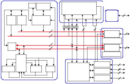
The discussion so far has involved the core architecture of the fixed-point ADSP21xx DSPs which is common to all members of the family. This section discusses the on-chip peripherals which have different configurations and options depending on the particular processor in the family. The ADSP-218x architecture is shown in Figure 7.14.
7.14
DSP HARDWARE
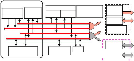
ADSP-218x FAMILY ARCHITECTURE
• Code Compatibility |
|
||
• Pin-for-Pin Compatibility |
|
|
|
POWERDOWN |
FULL MEMORY |
||
|
|||
|
CONTROL |
||
|
MODE |
||
|
|
||
ADSP-2100 CORE
DATA ADDRESS |
|
MEMORY |
PROGRAMMABLE |
EXTERNAL |
|||
PROGRAM |
PROGRAM |
DATA |
EXTERNAL I / O |
ADDRESS |
|||
GENERATORS |
|||||||
SEQUENCER |
and FLAG PINS |
BUS |
|||||
DAG1 |
DAG2 |
MEMORY |
MEMORY |
|
|||
|
|
|
|
EXTERNAL |
|||
|
|
|
|
|
PMA |
||
|
|
|
|
|
DATA BUS |
||
|
|
|
|
|
DMA |
BYTE DMA |
|
|
|
|
|
|
|
||
|
|
|
|
|
PMD |
CONTROLLER |
|
|
|
|
|
|
DMD |
OR |
|
|
|
|
|
|
|
EXTERNAL |
|
|
|
|
|
|
|
DATA BUS |
|
ARITHMETIC UNITS |
|
SERIAL PORTS |
|
TIMER |
|
|
|
|
|
|
|
|
|
|
|
|
|
|
|
|
|
|
|
||||
|
|
|
|
|
|
|
|
|
|
|
|
|
|
|
|
|
|
|
|||||||||
|
|
|
|
SPORT 0 |
SPORT 1 |
|
|
|
|
|
|
INTERNAL |
|
|
|
|
|
|
|||||||||
ALU |
MAC |
SHIFTER |
|
|
|
|
|
|
|
|
|
|
|
|
|
||||||||||||
|
|
|
|
|
|
|
|
|
|
|
|
|
|||||||||||||||
|
|
|
|
|
|
|
|
|
DMA PORT |
|
|
|
|
|
|
||||||||||||
|
|
|
|
|
|
|
|
|
|
|
|
|
|
|
|
|
|
|
|
|
|
|
|
|
|
|
|
|
|
|
|
|
|
|
|
|
|
|
|
|
|
|
|
|
|
|
|
|
|
|
|
|
|
|
|
HOST MODE
External bus features are multiplexed for 100-pin parts. All are available on 128-pin parts
Figure 7.14
ADSP-21xx ON-CHIP PERIPHERALS:
MEMORY INTERFACE
■All Family Members use an Enhanced Harvard Architecture
Separate Program Memory and Data Memory Spaces
Can access Data Values in Program Memory
■Different Family Members Have Different Memory Configurations
■External Memory Interface Supports Both Fast and Slow Memories with Programmable Wait States
■Supports DSP Boot Loading from Byte Memory Space or from a Host Processor
■Supports Memory-Mapped Peripherals Through I / O Space
■Bus Request / Grant Mechanism for Shared External Bus
Figure 7.15
7.15
DSP HARDWARE
The 21xx-family comes with a variety of on-chip memory options, and the newer 218x family has up to 48K words of program memory and 56K words of data memory. All family members use the modified Harvard architecture which provides separate program and data memory and allows data to be stored in program memory. The external memory interface supports both fast and slow memories with programmable wait states. The ADSP-218x family also supports memory-mapped peripherals through I/O space.
All 21xx parts (except the ADSP-2105) have two double-buffered serial ports (SPORTs) for transmitting or receiving serial data. Each SPORT is bi-directional, full duplex, double-buffered, and has its own programmable serial clock. The SPORT word length can be configured from 3 to 16 bits. Data can be framed or unframed. Each SPORT generates an interrupt and supports A-law and u-law companding.
ADSP-21xx ON-CHIP PERIPHERALS:
SERIAL PORTS (SPORTs)
■ADSP-21xx SPORTs Are Used For Synchronous Communication
■Full Duplex
■Fully Programmable
■Autobuffer/DMA Capability
■TDM Multi-Channel Capability
■A-law and u-law Companding
■Data Rates of 25 Mbits/sec and Above
■Glueless Interface to a Wide Range of Serial Peripherals or Processors
■219x DSPs Add SPI and UART Serial Ports (With Boot Capability)
Figure 7.16
The ADSP-218x-family internal direct-memory-access (IDMA) port supports booting from and runtime access by a host processor. This feature allows data to be transferred to and from internal memory in the background while continuing foreground processing. The IDMA port allows a host processor to access all of the DSPs internal memory without using mailbox registers. The IDMA port supports 16 and 24-bit words, and 24-bit transfers take two cycles to complete.
7.16
DSP HARDWARE
ADSP-21xx ON-CHIP PERIPHERALS:
INTERNAL DMA (IDMA)
■Allows an External System to Access DSP Internal Memory
■External Device or DSP Can Specify Internal Starting Address
■Address Automatically Increments to Speed Throughput
■16-Bit Bus Supports Both Data and Instruction Transfers (219x has 8-Bit Bus Support)
■Single DSP Processor-Cycle Transfers
■Supports Power-On Booting
Figure 7.17
The ADSP-218x-family also has a byte memory interface which supports booting from and runtime access to 8-bit memories. It can access up to 4MB. This memory space takes the place of the boot memory space found on other ADSP-21xx family processors. Byte memory consists of 256 pages of 16K x 8 locations. This memory can be written and read in 24-bit, 16-bit, or 8-bit left or right justified transfers. Transfers happen in the background to the DSP internal memory by stealing cycles.
ADSP-21xx ON-CHIP PERIPHERALS:
BYTE DMA PORT (BDMA)
■Provides Bulk Storage for Both Data and Program Code
■Can Access up to 4 Mbytes of External Code & Data
■Supports Multiple Data Formats
Automatic Data Packing/Unpacking to 16 and 24 bits
8-Bit Transfers, Leftor Right-Justified
■Background Transfer to DSP Internal Memory
One Cycle per Word
DSP Specifies Destination/Source and Word Count
■Supports Power-On Booting
■Allows Multiple Code Segments
DSP Can Overlay Code Sections
Processor Can Run During Transfer, or Halt and Restart
Figure 7.18
7.17
DSP HARDWARE
The ADSP-217x, ADSP-218x, and ADSP-21msp5x devices provide a powerdown feature that allows the processor to enter a very low power state (less than 1mW) through hardware or software control. This feature is extremely useful for batterypowered applications. During some of the powerdown modes, the internal clocks are disabled, but the processor registers and memory are maintained.
ADSP-21xx INTERNAL PERIPHERALS:
POWERDOWN
■Non-Maskable Interrupt
Hardware Pin (PWD), or Software Forced
■Holds Processor in CMOS Standby
■Rapid CLKIN-Cycle Recovery
■Acknowledge Handshake (PWDACK)
■Ideal for Battery-Powered Applications
■219x is Fully Static
Figure 7.19
From the above discussions it should be obvious that the ADI DSPs are designed for maximum efficiency when performing typical DSP functions such as FFTs or digital filtering. ADI DSPs can perform several operations in an instruction cycle as has been shown in the above filter example. DSPs are often rated in terms of Millions of Instructions per Second, or MIPS. However, the MIPS rating does not tell the entire story. For example if processor A has a instruction rate of 50 MIPS and can perform 1 operation per instruction, it can perform 50 Million Operations per Second, or 50 MOPS. Now assume that processor B has an instruction rate of 20 MIPS, but can perform 4 operations per instruction. Processor B can therefore perform 80 Million Operations per Second, or 80 MOPS, and is actually more efficient than processor A. A better way to evaluate DSP performance is to use well defined benchmarks such an FIR filter with a prescribed number of taps or an FFT of known size. Benchmark comparisons eliminate the confusion often associated with MIPS or MOPS ratings alone and are discussed later in this section. Even this form of benchmarking does not give a true comparison of performance between two processors. Analysis of the target system requirements, processor architecture, memory needs and other factors must be considered.
7.18
DSP HARDWARE
The ADSP-219x family maintains code compatibility with the ADSP-218x. Streamlined for faster processing and improved C-compiler efficiency, this new family will include DSPs with speeds between 100 and 300MIPS and power consumption as low as 0.4mA/MIP. JTAG support is also included to provide a more robust software emulation and test capability. A block diagram of the family is shown in Figure 7.20.
ADSP-219x SERIES ARCHITECTURE
ADSP-219x |
Instr. |
|
Internal |
|
||
Processor Core |
Cache |
Memory System |
|
|||
Register |
|
|
|
|||
DAG1 |
DAG2 |
Seq. |
Program |
PM |
DM |
JTAG & |
|
Sequencer |
EMULATION |
||||
PMA |
|
|
24 |
|
|
|
|
|
24 |
|
|
EXTERNAL |
|
DMA |
|
|
|
|
||
PMD |
|
|
24 |
|
|
MEMORY |
|
|
16 |
|
|
INTERFACE |
|
DMD |
|
|
|
|
||
|
|
|
|
|
|
|
DATA REGISTERS
ALU 
 MAC
MAC 
 Shift
Shift
Computational Units
DMA INTERFACE
PERIPHERAL AND
■Improved addressing (14-bit reach increased to 24-bit reach)
■Compiler-efficient data register design
■Program sequencer with Cache for fast code execution
■JTAG support for easy development
Figure 7.20
The address reach of the ADSP-219x series has been extended from the ADSP218x’s 14-bit reach to a 24-bit reach. This supports 64K word direct memory addressing or 16M word paged memory addressing. All existing addressing modes are supported, and five new DAG addressing modes have been added.
Many of the enhancements in the ADSP-219x are designed to improve compiler efficiency. A global register allocator and support for register file-like operand access reduces spills and reduces reliance on the local stack. The compiler features DSP intrinsic support including fractional and complex. On-chip cache memory has also been added.
The ADSP-219x core will serve as a key DSP technology for ADI’s 16-bit general purpose DSP offerings, and embedded DSP solutions, where application-specific circuitry and software are custom-designed to a customer’s precise requirements.
For performance-driven applications, multiple cores will be integrated together on a single die. In the future, four cores will be combined in a family of devices capable of delivering 1.2 billion MACs per second per square inch. Power-conscious designers will appreciate operating currents of 0.15mA/MIPS.
7.19
DSP HARDWARE
ADSP-219x FAMILY KEY SPECIFICATIONS
Code Compatible
Compatible with ADSP-218x Series
Single Cycle Instruction Execution, Zero-Over Head Looping, Single Cycle Context Switch
Performance
Architectural Performance Beyond 300 MIPs.
Fully Transparent Instruction Cache
Compiler-Friendly and Tool-Friendly
64K Word Direct and 16 Mword Paged Memory Support
5 New DAG Addressing Modes
Register File-Like Operand Access
JTAG Interface Support
Figure 7.21
The history of the Analog Devices 16-bit fixed-point DSP family is shown in Figure 7.22. Notice the migration in performance as well as improvements in power dissipation and packaging while maintaining code compatibility between the various devices. The newer families offer 3.3V (L-series) and 2.5V (M-series) operation for further efficiency. Earlier DSPs were packaged in expensive pin-grid- array (PGA) packages or plastic-leaded-chip-carriers (PLCCs), but these have been largely replaced by plastic-quad-flat-packs (PQFPs), and more recently by thin (1.6mm) quad-flat-packs (TQFPs). Note: In 1998, JEDEC changed the specifications for the TQFP package designation, assigning it to packages 1.0mm thick. Previously labeled TQFP packages (1.6mm thick) are now designated as LQFP per the JEDEC specification.
The 144-ball miniBGA package (see Figure 7.23) from ADI represents innovative packaging combined with low power consumption (0.4mA per MIP), and allows 75MIPS operation and more than 2M bits of SRAM in a 1cm2 package which is 1.35mm thick. For example, the 75MIPS ADSP-2188M has 48K of 24-bit program memory and 56K of 16-bit data memory for a total of 48K×24 + 56K×16 = 2028K bits with a power dissipation of less than 100mW.
7.20
DSP HARDWARE
16-BIT DSP FAMILY TREE: HISTORY OF IMPROVEMENTS IN PACKAGING - POWER - PERFORMANCE
 Performance
4.45mm thick
PLCC
20 MIPS 216x
2K/1K RAM
210x
|
|
|
|
|
|
|
|
|
miniBGA |
|
|||
|
|
1.6mm thick |
|
|
|
|
|
|
150-300 MIPS |
||||
|
|
|
|
|
|
|
|
|
|
|
|
|
0.4 mA/MIPs |
|
|
|
LQFP |
|
|
|
|
|
|
|
219x |
||
|
|
|
|
|
|
p |
ati |
b |
le |
-BGA |
2188M |
||
|
|
|
|
|
|
|
|||||||
|
|
|
|
|
|
|
|
|
|||||
|
|
|
n C |
o |
m |
|
|
Mini |
2189M |
||||
|
|
Pi |
|
|
|
||||||||
|
|
&144Ball |
|
|
|
||||||||
|
100 |
Pin |
LQFP |
2185/L/M |
|
|
“L” = 3.3V |
||||||
|
|
|
|
|
|||||||||
|
|
|
|
|
|
||||||||
21msp5x |
|
|
2186/L/M |
|
|
|
|
|
|
“M” = 2.5V |
|||
|
2184/L |
|
|
|
|
|
33 - 75 MIPS |
“N” = 1.8V |
|||||
2111 |
2181/3 |
|
|
|
|
|
|
0.4 mA/MIPS |
|
||||
|
|
|
|
|
|
|
|
|
|
|
|||
33 MIPS |
|
|
PQFP |
|
2.45mm thick |
|
|||||||
2K/2K RAM |
|
|
|
|
|
|
|
|
|
|
|
|
|
Code Compatible
Figure 7.22
‘M’ SERIES OFFERS THE LARGEST MIPS/MEMORY DENSITY WITH miniBGA PACKAGING!!!
1.35mm Thick
10mm
10mm
|
■ 75 MIPS and >2Mbit in 1cm2 |
|
■ Small size with no compromises in |
|
performance: 144-balls |
|
■ Up to 2 Mbits on-chip SRAM |
|
■ Innovative packaging for highly |
|
portable applications |
0.8mm |
■ Small package size and 0.4mA per MIP |
Pitch |
targets power-sensitive applications |
miniBGA package |
■ Includes ALL ‘M’ series members plus |
144-ball grid array (BGA) |
the popular 2183, 2185L, 2186, & 2186L |
|
derivatives |
|
Figure 7.23 |
7.21
DSP HARDWARE
ADI 16-Bit DSP ROADMAP
16 Years of Code Compatibility & Beyond 219x Core
|
|
|
218x Core |
600 - 1200 MIPS |
|
1000 |
Multiple Core |
|
16M - 128MBits |
||
|
|
|
|
||
|
Devices |
312 - 600 MIPS |
• As Low as 0.5mW/MIPS |
||
|
|
8M - 16MBits |
|||
|
|
|
• As High as 8MIPs/mm2 |
||
500 |
|
• As Low as 0.7mW/MIPS |
|
||
|
2100 Core |
• As High as 0.5MIP/mm2 |
|
||
|
|
|
Compatibility |
|
|
|
|
|
Code |
150-300 MIPS |
|
|
|
|
|
||
|
Complete |
|
|
640K - 32MBits |
|
100 |
|
|
|
||
|
|
29-80 MIPS |
|
||
|
|
|
• As Low as 0.4mW/MIPS |
||
MMACs |
|
|
160K - 2MBits |
||
10 - 33 MIPS |
|
• As High as 3MIPs/mm2 |
|||
|
|
|
Single Core |
||
32K - 80KBits |
• |
As Low as 0.6mW/MIPS |
|||
|
|||||
• As Low as 6mW/MIPS |
• As High as 0.8MIP/mm2 |
Devices |
|||
|
|
|
|||
• As High as 0.1MIP/mm2 |
|
|
|
|
|
|
1985 |
|
|
|
2000+ |
Figure 7.24
|
ADSP-218x ROADMAP |
|
||||
|
|
|
|
|
1.8V |
|
|
|
2.5V |
|
600 MIPS |
Multiple |
|
|
|
|
Core |
|||
|
|
|
|
|
16MBits |
|
500 |
|
|
|
|
SRAM |
Devices |
|
600 MIPS |
|
• 0.7mW/MIPS |
|||
|
|
|
||||
|
5/3.3V |
16MBits |
|
• 0.5MIPs/mm2 |
|
|
|
|
SRAM |
|
|
|
|
|
312 MIPS |
• 1mW/MIPS |
|
|
|
|
|
8MBits |
• 0.5MIP/mm2 |
|
|
||
|
SRAM |
|
|
|
Options |
|
|
• 2.6mW/MIPS |
|
|
|
|
|
|
|
&Pin |
Compatible |
1.5V |
||
100 |
• 0.3MIP/mm2 |
|
||||
|
Code |
|
80 MIPS |
|||
|
|
|
|
640K -2MBits |
|
|
|
|
|
75 MIPS |
|
SRAM |
|
|
|
|
|
|
|
|
MMACs |
|
320K - 2MBits |
•As Low as 0.7mW/MIPS |
40 MIPS |
||
29-52 MIPS |
|
SRAM |
|
•As High as 0.8MIPs/mm2 |
640K -2MBits |
|
160K- 1.2MBits |
|
|
|
Single Core |
SRAM |
|
SRAM |
•As Low as 1mW/MIPS |
•As Low as 0.6mW/MIPS |
||||
• As Low as 2.6mW/MIPS |
•As High as 0.75MIP/mm2 |
|||||
|
|
|
Devices |
•As High as 0.4MIPs/mm2 |
||
• As High as 0.5MIP/mm2 |
|
|
|
|
||
|
1994 |
|
|
|
2000+ |
|
Figure 7.25
7.22
DSP HARDWARE
ADSP-219x ROADMAP
1000
500
100
MMACs
218x to 219x 16 Years of continuing code compatible architectures!
ADSP-218X
<2000
ADSP-219x
320 MIPS
ADSP-2191
160 MIPS
 0.5 mW / MIPS
 2.5V
2.5V 
|
|
|
|
ADSP-219x |
|||
|
|
|
|
1200 MIPS |
|||
ADSP-219x |
|
|
|
-Core |
|||
|
Multiple |
||||||
600 MIPS |
|
|
|||||
|
Performance |
|
|
||||
Highest |
|
|
|
ADSP-219x |
|||
|
|
|
300 MIPS |
||||
ADSP-219x |
|
|
|
|
|
-Core |
|
|
|
|
|
Single |
|||
200 MIPS |
|
Performance |
|||||
|
|
|
|||||
High |
|
|
|||||
|
ADSP-219x |
||||||
ADSP-219x |
|
|
0.05 mW / MIPS |
||||
|
|
|
1.0V |
||||
0.1 mW / MIPS |
|
||||||
|
|
|
|
||||
1.5V |
|
|
|
|
|
|
-Core |
|
|
|
|
|
|
|
|
Power |
Efficient |
Single |
|||||
|
|
|
|||||
|
|
|
|
|
|
||
|
|
|
|
|
|
|
|
|
|
|
|
|
|
2000 |
2001 |
2002 |
2003 |
||
Figure 7.26
FIXED-POINT VERSUS FLOATING POINT
DSP arithmetic can be divided into two catagories: fixed-point and floating-point. These refer to the format used to store and manipulate the numbers within the devices. The Analog Devices’ fixed-point DSPs such as those discussed so far represent each number with 16 bits. There are four common ways that 216 = 65,536 possible bit patterns can represent a number. In unsigned integer format, the stored number takes on any integer value from 0 to 65,536. In signed integer format, two’s complement is used to make the range include negative numbers, from –32,768 to +32,767. Using unsigned fractional format, the 65,536 levels are spread uniformly between 0 and +1. Finally, signed fractional format allows negative numbers, with 65,536 levels equally spaced between –1 and +1.
The ADSP-21xx family arithmetic is optimized for the signed fractional format denoted by 1.15 (“one dot fifteen”). In the 1.15 format, there is one sign bit (the MSB) and fifteen fractional bits representing values from –1 up to 1 LSB less than +1 as shown in Figure 7.27.
7.23

DSP HARDWARE
16-BIT FIXED POINT ARITHMETIC FRACTIONAL 1.15 FORMAT
MSB |
|
|
|
|
|
|
|
|
|
|
BIT WEIGHT |
|
|
|
|
|
|
|
LSB |
|||||||
|
|
|
|
|
|
|
|
|
|
|
|
|
|
|
|
|
|
|
|
|
|
|||||
–20 |
|
2–1 |
|
2–2 |
|
2–3 |
2–4 |
2–5 |
2–6 |
2–7 |
|
2–8 |
2–9 |
2–10 |
2–11 |
2–12 |
2–13 |
2–14 |
2–15 |
|||||||
|
|
|
|
|
|
|
|
|
|
|
|
|
|
|
|
|
|
|
|
|||||||
|
|
|
|
|
|
|
|
|
|
|
|
|
|
|
|
|
|
|
|
|||||||
|
|
|
|
|
|
HEX |
|
|
|
|
|
BINARY |
|
|
|
|
|
DECIMAL |
||||||||
|
|
|
|
|
|
|
|
|
|
|
|
|
|
|
|
|||||||||||
|
|
|
|
|
|
|
|
|
|
|
|
|
|
|
|
|
|
|
|
|
|
|
|
|
|
|
|
|
|
|
|
7FFF |
|
|
0111 |
1111 |
1111 |
1111 |
|
+0.999969 |
|
|
|||||||||||
|
|
|
|
|
|
|
|
|
|
|
|
|
|
|
|
|
||||||||||
|
|
|
|
|
0001 |
|
|
|
0000 |
0000 |
0000 |
0001 |
|
+0.000031 |
|
|
||||||||||
|
|
|
|
|
|
|
|
|
|
|
|
|
|
|
|
|
||||||||||
|
|
|
|
|
0000 |
|
|
|
0000 |
0000 |
0000 |
0000 |
|
+0.000000 |
|
|
||||||||||
|
|
|
|
|
|
|
|
|
|
|
|
|
|
|
|
|||||||||||
|
|
|
|
|
FFFF |
|
|
1111 |
1111 |
1111 |
1111 |
|
|
–0.000031 |
||||||||||||
|
|
|
|
|
|
|
|
|
|
|
|
|
|
|
|
|
||||||||||
|
|
|
|
|
8000 |
|
|
|
1000 |
0000 |
0000 |
0000 |
|
|
–1.000000 |
|||||||||||
|
|
|
|
|
|
|
|
|
|
|
|
|
|
|
|
|
|
|
|
|
|
|
|
|
|
|
Figure 7.27
This convention can be generalized as “I.Q”, in which I is the number of bits to the left of the radix point, and Q is the number of bits to the right. For example, full unsigned integer number representation is 16.0 format. For most signal processing applications, however, fractional numbers (1.15) are assumed. Fractional numbers have the advantage that the product of two fractional numbers is smaller than either of the numbers.
By comparison, floating point DSPs typically use a minimum of 32 bits to represent each number. This results in many more possible numbers than for 16-bit fixed point, 232 = 4,294,967,296 to be exact. More importantly, floating point greatly increases the range of values that can be expressed. The most common floating point standard is ANSI/IEEE Standard 754-1985, where the largest and smallest numbers allowed by the standard are ±3.4×1038 and ±1.2×10–38, respectively. Note that the 754 standard reserves some of the possible range to free up bit patterns which allow other special classes of numbers such as ±0 and ±∞, for example.
The IEEE-754 floating point standard is described in more detail in Figure 7.28. The 32-bit word is divided into a sign bit, S, an 8-bit exponent, E, and a 23-bit mantissa, M. The relationship between the decimal and binary IEEE-754 floating point equivalent is given by the equation:
NUMBER10 = (−1)S ×1.M × 2(E−127) .
Notice that the “1.” is assumed to precede the “M”, and that a “bias” of 127 is subtracted from the exponent “E” so that “E” is always a positive number.
7.24
DSP HARDWARE
SINGLE PRECISION IEEE-754 32-BIT FLOATING POINT FORMAT,
|
|
|
|
|
|
|
|
|
|
NUMBER10 = (–1)S × 1.M × 2(E–127) |
Bias |
|||||||||||||||||||||||||||
|
|
|
|
|
|
|
|
|
|
|
|
|
|
|
||||||||||||||||||||||||
|
|
|
|
|
|
|
|
|
|
|
|
|
|
|
|
|
|
|
|
|
|
|
|
|
|
|
Assumed |
|
|
|
|
|
||||||
|
|
|
|
MSB |
|
|
|
|
|
|
|
|
|
|
|
|
|
|
|
LSB |
|
MSB |
|
|
|
|
|
|
|
|
|
|
|
LSB |
||||
|
|
|
|
|
|
|
|
|
|
|
|
|
|
|
|
|
|
|
|
|
|
|
|
|
|
|
|
|
|
|
||||||||
|
0/1 |
|
27 |
|
26 |
|
|
25 |
|
24 |
|
23 |
|
22 |
21 |
20 |
|
2–1 |
|
2–2 |
2–3 |
|
2–4 |
|
|
2–22 |
2–23 |
|
||||||||||
|
|
|
|
|
|
|
|
|
|
|
|
|
|
|
|
|
|
|
|
|
|
|
||||||||||||||||
|
SIGN |
|
|
EXPONENT = E |
|
|
|
|
|
|
|
|
|
|
|
|
MANTISSA = M |
|
||||||||||||||||||||
|
|
|
|
|
|
|
|
|
|
|
|
|
|
|
|
|
|
|||||||||||||||||||||
BIT = S |
|
|
|
|
|
8-BITS |
|
|
|
|
|
|
|
|
|
|
|
|
23-BITS |
|
|
|
|
|
||||||||||||||
|
|
|
|
|
|
|
|
|
|
|
|
|
|
|
|
|
|
|
|
|
|
|
|
|
|
|
|
|
|
|
|
|
|
|
|
|
||
0 |
|
00000111 |
1100…00 |
|
|
|
|
|
|
|
|
Bias |
|
|
|
|
|
|
|
|||||||||||||||||||
|
|
|
|
|
|
|
|
|
|
|
|
|
|
|
|
|
|
|
||||||||||||||||||||
|
+ 1.75 × 2(7–127) |
|
|
+ 1.316554 × 10–36 |
||||||||||||||||||||||||||||||||||
+ |
|
7 |
|
|
|
|
|
|
0.75 |
|
|
|
|
= |
||||||||||||||||||||||||
|
|
|
|
|
|
|
|
|
|
|
|
|
|
|
|
|
|
|
|
|
|
Assumed |
|
|
|
|
|
|
|
|
|
|||||||
1 |
|
10000001 |
|
0110…00 |
|
|
|
|
|
|
|
|
|
|
|
|
Bias |
|
|
|
|
|
||||||||||||||||
|
|
– 1.375 × 2(129–127) = |
|
|
|
|
|
|
|
|||||||||||||||||||||||||||||
|
– |
129 |
|
|
|
|
0.375 |
|
|
|
– 5.500000 |
|||||||||||||||||||||||||||
|
|
|
|
|
|
|
|
|
|
|
|
|
|
|
|
|
|
|
|
|
|
|
|
|
|
|
|
|
|
|
|
|
|
|
|
|
|
|
 Assumed
Figure 7.28
In the case of extended precision floating point arithmetic, there is one sign bit, the mantissa is 31-bits, the exponent is 11-bits, and the total word length is 43-bits.
Extended precision thus adds 8 bits of dynamic range to the mantissa and can execute almost as fast as single precision, since accumulators can readily be extended beyond 32 bits. On the other hand, true 64-bit double precision (52-bit mantissa, 11-bit exponent, and 1 sign bit) requires extra processor cycles. Requirements for double precision are rare in most DSP applications.
Many DSP applications can benefit from the extra dynamic range provided by 32-bit floating point arithmetic. In addition, programming floating point processors is generally easier, because fixed-point problems such as overflow, underflow, data scaling, and round-off error are minimized, if not completely eliminated. Although the floating point DSP may cost slightly more than the fixed point DSP, development time may well be shorter with floating point.
While all floating point DSPs can also handle fixed point numbers (required to implement counters, loops, and ADC/DAC signals), this doesn’t necessarily mean that fixed point math will be carried out as quickly as the floating point operations; it depends on the internal DSP architectures. For instance, the SHARC DSPs from Analog Devices are optimized for both floating point and fixed point operations, and execute them with equal efficiency. For this reason, the SHARC devices are often referred to as “32-bit DSPs” rather than just “Floating Point.”
7.25
DSP HARDWARE
FIXED POINT VS. FLOATING POINT ARITHMETIC
16-Bit Fixed-Point:
216 = 65,536 Possible Numbers |
|
|
32-Bit Floating Point: |
|
|
Biggest Number: ±6.8 × 1038 |
754 |
Std: ±3.4 × 1038 |
Smallest Number: ±5.9 × 10–39 |
754 |
Std: ±1.2 × 10–38 |
Extended-Precision (40-Bits: Sign + |
8-Bit Exponent + 31-Bit Mantissa) |
|
Double-Precision (64-Bits: Sign + 11-Bit Exponent + 52-Bit Mantissa)
32-Bit Floating Point
More Precision
Much Larger Dynamic Range
Easier to Program
Figure 7.29
ADI SHARC® FLOATING POINT DSPS
The ADSP-2106x Super Harvard Architecture SHARC is a high performance 32-bit DSP. The SHARC builds on the ADSP-21000 family DSP core to form a complete system-on-a-chip, adding a dual-ported on-chip SRAM and integrated I/O peripherals supported by a dedicated I/O bus. With its on-chip instruction cache, the processor can execute every instruction in a single cycle. Four independent buses for dual data, instructions, and I/O plus crossbar switch memory connections comprise the Super Harvard Architecture of the ADSP-2106x shown in Figure 7.30.
A general purpose data register file is used for transferring data between the computation units and the data buses, and for storing intermediate results. The register file has two sets (primary and alternate) of 16 registers each, for fast context switching. All of the registers are 40 bits wide. The register file, combined with the core processor’s super Harvard architecture, allows unconstrained data flow between computation units and internal memory.
The ADSP-2106x SHARC processors address the five central requirements for DSPs established in the ADSP-21xx family of 16-bit fixed point DSPs: (1) fast, flexible arithmetic computation units, (2) unconstrained data flow to and from the computation units, (3) extended precision and dynamic range in the computation units, (4) dual address generators, and (5) efficient program sequencing with zerooverhead looping.
The program sequencer includes a 32-word instruction cache that enables three-bus operation for fetching an instruction and two data values. The cache is selective – only instructions whose fetches conflict with program memory data accesses are cached. This allows full-speed multiply-accumulates and FFT butterfly processing.
7.26
DSP HARDWARE
ADI SUPER HARVARD ARCHITECTURE (SHARC®) 32-BIT DSP ARCHITECTURE FOR ADSP-2106x FAMILY
CORE |
|
INSTRUCTION |
|
TWO INDEPENDENT |
0 |
DUAL PORTED SRAM |
|
|||||||||
TIMER |
|
BLOCK |
|
|||||||||||||
PROCESSOR |
|
CACHE |
|
DUAL-PORTED BLOCKS |
1 |
|
|
|
||||||||
|
32x48 BIT |
PROCESSOR PORT |
I/O PORT |
|
|
|
||||||||||
|
|
|
|
|
|
ADDR |
DATA |
DATA |
ADDR |
BLOCK |
JTAG |
7 |
|
|||
|
|
|
|
|
|
|
|
|
|
|
|
|
TEST & |
|
|
|
DAG1 |
DAG2 |
|
PROGRAM |
ADDR |
DATA |
DATA |
ADDR |
EMULATION |
|
|||||||
|
|
|
|
|
|
|
|
|
|
|
|
|||||
8x4x32 |
8x4x24 |
|
SEQUENCER |
|
|
|
|
|
|
|
|
|
|
|
||
|
|
|
|
|
|
|
|
|
|
|
IOD |
|
IOA EXTERNAL PORT |
|
||
|
|
PMA |
|
24 |
|
|
|
|
|
48 |
|
17 |
ADDR BUS |
32 |
||
|
|
|
|
|
|
|
|
|
|
|
|
|
|
|||
|
|
DMA |
|
32 |
|
|
|
|
|
|
|
|
|
|||
|
|
|
|
|
|
|
|
|
|
|
MUX |
|
|
|||
|
|
|
|
|
|
|
|
|
|
|
|
|
MULTIPROCESSOR |
|
||
BUS |
|
PMD |
|
48 |
|
|
|
|
|
|
|
|
INTERFACE |
|
||
|
|
|
|
|
|
|
|
|
|
DATA BUS |
48 |
|||||
Connect |
|
DMD |
|
40 |
|
|
|
|
|
|
|
|
||||
|
|
|
|
|
|
|
|
|
|
|
||||||
(PX) |
|
|
|
|
|
|
|
|
|
|
MUX |
|
|
|||
|
|
|
|
|
|
|
|
|
|
|
|
|
|
|
||
|
|
|
|
|
|
|
|
|
|
|
|
|
|
HOST PORT |
|
|
|
DATA |
|
|
|
|
|
|
|
|
|
|
|
|
|
|
|
|
REGISTER |
|
|
|
|
|
|
|
|
|
|
|
DMA |
|
4 |
|
|
FILE |
|
|
|
|
|
P |
|
D |
E |
I |
|
|
|
||
|
16x40 |
|
|
|
|
|
|
|
CONTROLLER |
|
|
|||||
|
BARREL |
|
|
|
M |
|
M |
P |
O |
|
|
|
||||
|
BIT |
|
|
|
|
|
|
|
6 |
|
||||||
MULTIPLIER |
|
ALU |
|
D |
|
D |
D |
D |
SERIAL PORTS |
|
||||||
|
|
SHIFTER |
|
|
|
|
|
|
|
6 |
|
|||||
|
|
|
|
|
|
|
IOP REGISTERS |
|
|
(2) |
|
|
||||
|
|
|
|
|
|
|
(Memory Mapped) |
|
LINK PORTS |
36 |
|
|||||
|
|
|
|
|
|
|
Control, Status, |
|
|
|
||||||
|
|
|
|
|
|
|
and Data Buffers |
|
|
(6) |
|
|
|
|||
I/O PROCESSOR
Figure 7.30
SHARC KEY FEATURES
■100MHz Core / 300 MFLOPS Peak
■Parallel Operation of: Multiplier, ALU, 2 Address Generators & Sequencer
No Arithmetic Pipeline; All Computations Are Single-Cycle
■High Precision and Extended Dynamic Range
32/40-Bit IEEE Floating-Point Math
32-Bit Fixed-Point MAC’s with 64-Bit Product & 80-Bit Accumulation
■Single-Cycle Transfers with Dual-Ported Memory Structures
Supported by Cache Memory and Enhanced Harvard Architecture
■Glueless Multiprocessing Features
■JTAG Test and Emulation Port
■DMA Controller, Serial Ports, Link Ports, External Bus, SDRAM Controller, Timers
Figure 7.31
7.27

DSP HARDWARE
SHARC® THE LEADER IN FLOATING POINT DSP
■SHARC is the de facto standard in multiprocessing
■ADSP-21160 continues SHARC leadership in multiprocessing
■ADSP-21065L is the right choice for low-cost floating point
SUPER HARVARD ARCHITECTURE:
Balancing Memory, I/O and Computational
Power...
■High Performance Computation Unit
■Four Bus Performance
Fetch Next Instruction
Access 2 data values
Perform DMA for I/O
■Memory Architecture
■Non Intrusive DMA
Figure 7.32
The ADSP-2106x family execute all instructions in a single cycle. They handle 32-bit IEEE floating point format, 32-bit integer and fractional fixed point formats (twoscomplement and unsigned), and extended precision 40-bit IEEE floating point format. The processors carry extended precision throughout their computation units, minimizing intermediate data truncation errors. When working with data onchip, the extended precision 32-bit mantissa can be transferred to and from all computation units. The 40-bit data bus may be extended off-chip if desired. The fixed point formats have an 80-bit accumulator for true 32-bit fixed point computations.
The ADSP-2106x has a super Harvard architecture combined with a 10-port data register file. In every cycle, (1) two operands can be read or written to or from the register file, (2) two operands can be supplied to the ALU, (3) two operands can be supplied to the multiplier, and (4) two results can be received from the ALU and multiplier.
The ADSP-2106x family instruction set provides a wide variety of programming capabilities. Multifunction instructions enable computations in parallel with data transfers, as well as simultaneous multiplier and ALU operations.
7.28
DSP HARDWARE
The ADSP-21060 contains 4 Mbits of on-chip SRAM, organized as two blocks of 2 Mbits each, which can be configured for different combinations of code and data storage. The ADSP-21062, ADSP-21061 and ADSP-21065 each include 2 Mbit, 1Mbit and 544Kbits of on-chip SRAM, respectively. Each memory block is dualported for single-cycle, independent accesses by the core processor and I/O processor or DMA controller. The dual-ported memory and separate on-chip buses allow two data transfers from the core and one from I/O, all in a single cycle.
While each memory block can store combinations of code and data, accesses are most efficient when one block stores instructions and data, using the DM bus for transfers, and the other block stores instructions and data, using the PM bus for transfers. Using the DM bus and PM bus in this way, with one dedicated to each memory block, assures single-cycle execution with two data transfers. In this case, the instruction must be available in the cache. Single-cycle execution is also maintained when one of the data operands is transferred to or from off-chip, via the ADSP-2106x’s external port.
The ADSP-2106x’s external port provides the processor’s interface to off-chip memory and peripherals. The 4 Gword off-chip address space is included in the ADSP-2106x’s unified address space. The separate on-chip buses – for PM addresses, PM data, and DM addresses, DM data, I/O addresses, and I/O data – are multiplexed at the external port to create an external system bus with a single 32bit address bus and a single 48-bit data bus. The ADSP-2106x provides programmable memory wait states and external memory acknowledge controls to allow interfacing to DRAM and peripherals with variable access, hold, and disable time requirements.
The ADSP-2106x’s host interface allows easy connection to standard microprocessor buses, both 16-bit and 32-bit, with little additional hardware required. Four channels of DMA are available for the host interface; code and data transfers are accomplished with low software overhead. The host can directly read and write the internal memory of the ADSP-2106x, and can access the DMA channel setup and mailbox registers. Vector interrupt support is provided for efficient execution of host commands.
The ADS-2106x offers powerful features tailored to multiprocessing DSP systems. The unified address space allows direct interprocessor accesses of each ADSP2106x’s internal memory. Distributed bus arbitration logic is included on-chip for simple, glueless connection of systems containing up to six ADSP-2106xs and a host processor. Master processor changeover incurs only one cycle of overhead. Bus arbitration is selectable as either fixed or rotating priority. Maximum throughput for interprocessor data transfer is 240 Mbytes/second (with a 40MHz clock) over the link ports or external port.
The ADSP-2106x’s I/O Processor (IOP) includes two serial ports, six 4-bit link ports, and a DMA controller. The ADSP-2106x features two synchronous serial ports that provide an inexpensive interface to a wide variety of digital and mixed-signal peripheral devices. The serial ports can operate at the full external clock rate of the processor, providing each with a maximum data rate of 50 Mbit/second. Independent transmit and receive functions provide greater flexibility for serial communications. Serial port data can be automatically transferred to and from on-
7.29
DSP HARDWARE
chip memory via DMA. Each of the serial ports offers a TDM multichannel mode. They offer optional µ-law or A-law companding. Serial port clocks and frame syncs can be internally or externally generated.
The ADSP-21060 and ADSP-21062 feature six 4-bit link ports that provide additional I/O capabilities. The link ports can be clocked twice per cycle, allowing each to transfer 8 bits per cycle. Link port I/O is especially useful for point-to-point interprocessor communication in multiprocessing systems. The link ports can operate independently and simultaneously, with a maximum data throughput of 240 Mbytes/second. Link port data is packed into 32-bit or 48-bit words, and can be directly read by the core processor or DMA-transferred to on-chip memory. Each link port has its own double-buffered input and output registers. Clock/acknowledge handshaking controls link port transfers. Transfers are programmable as either transmit or receive. There are no link ports on the ADSP-21061 or ADSP-21065 devices.
The ADSP-2106x’s on-chip DMA controller allows zero-overhead data transfers without processor intervention. The DMA controller operates independently and invisibly to the processor core, allowing DMA operations to occur while the core is simultaneously executing its program. Both code and data can be downloaded to the ADSP-2106x using DMA transfers. DMA transfers can occur between the ADSP2106x’s internal memory and external memory, external peripherals, or a host processor. DMA transfers can also occur between the ADSP-2106x’s internal memory and its serial ports or link ports. DMA transfers between external memory and external peripheral devices are another option.
The internal memory of the ADSP-2106x can be booted at system powerup from an 8-bit EPROM or a host processor. Additionally, the ADSP-21060 and the ADSP21062 can also be booted through one of the link ports. Both 32-bit and 16-bit host processors can be used for booting.
The ADSP-2106x supports the IEEE standard P1149.1 Joint Test Action Group (JTAG) standard for system test. This standard defines a method for serially scanning the I/O status of each component in a system. In-circuit emulators also use the JTAG serial port to access the processor’s on-chip emulation features. EZ-ICE Emulators use the JTAG test access port to monitor and control the target board processor during emulation. The EZ-ICE in-circuit emulator provides full-speed emulation to enable inspection and modification of memory, registers, and processor stacks. Use of the processor’s JTAG interface assures non-intrusive in-circuit emulation – the emulator does not affect target system loading or timing.
The SHARC architecture avoids processor bottlenecks by balancing core, memory, I/O processor, and peripherals as shown in Figure 7.30. The core supports 32-bit fixed and floating point data. The memory contributes to the balance by offering large size and dual ports. The core can access data from one port, and the other port is used to move data to and from the I/O processor. The I/O processor moves data to and from the peripherals to the internal memory using zero overhead DMAs. These operations run simultaneously to the core operation.
7.30

DSP HARDWARE
ADSP-2116X SINGLE-INSTRUCTION, MULTIPLE-
DATA (SIMD) CORE ARCHITECTURE
The ADSP-21160 is the first member of the second-generation ADI 32-bit DSPs. Its core architecture is shown in Figure 7.33. Notice that the core is similar to the ADSP-2106x core except for the width of the buses and the addition of a second computational unit complete with its own multiplier, ALU, shifter, and register file. This architecture is called single-instruction, multiple-data (SIMD) as opposed to single-instruction, single-data (SISD). The second computational unit allows the DSP to process multiple data streams in parallel. The core operates at up to 100 MIPS. At 100MHz clock operation the core is capable of 400 MFLOPS (millions of floating point operations per second) sustained and 600 MFLOPS peak operation. SIMD is a natural next step in increasing performance for ADI DSPs. Because their basic architecture already allows single instruction and multiple data access, adding another computational unit lets the architecture process the multiple data. The SIMD architectural extension allows code-compatible higher performance parts.
ADSP-2116x CORE PROCESSOR FEATURING
SINGLE-INSTRUCTION, MULTIPLE-DATA (SIMD)
|
TIMER |
INSTRUCTION |
|
|
|
|
CACHE |
|
|
|
|
32x48 BIT |
ADSP-2116x |
|
|
|
|
||
DAG1 |
DAG2 |
PROGRAM |
CORE PROCESSOR |
|
|
||||
8x4x32 |
8x4x32 |
SEQUENCER |
|
|
|
PMA |
32 |
||
|
DMA |
32 |
||
BUS |
PMD |
16/32/40/48/64 |
||
|
|
|
||
Connect |
DMD |
32/40/64 |
||
(PX) |
||||
|
|
|
||
|
DATA |
|
|
|
|
REGISTER |
|
|
|
|
FILE |
|
|
|
|
(PEx) |
|
|
|
MULTIPLIER |
16x40 |
BARREL |
ALU |
|
BIT |
||||
SHIFTER |
||||
|
|
|
|
DATA |
|
|
|
|
REGISTER |
|
|
|
|
FILE |
|
|
|
|
(PEy) |
|
|
|
MULTIPLIER |
16x40 |
BARREL |
ALU |
|
BIT |
||||
SHIFTER |
||||
|
|
|
Figure 7.33
7.31
DSP HARDWARE
The SIMD features of the ADSP-2116x include two computational units (PEx, PEy) and double data-word size buses (DMD and PMD). The primary processing element, PEx, is always enabled. The secondary processing element, PEy, is mode control enabled. The double wide data buses provide each computational unit with its own data set in each cycle. With SIMD enabled, both processing elements execute the same instruction each cycle (that’s the Single-Instruction), but they execute that instruction using different data (that’s the Multiple-Data). The SIMD-based performance increase appears in algorithms that can be optimized by splitting the processing of data between the two computational units. By taking advantage of the second computational unit the cycle time can be cut in half compared to the SISD approach for many algorithms.
The ADSP-21160 has a complete set of integrated peripherals: I/O Processor, 4 Mbyte on-chip dual-ported SRAM, glueless multiprocessing features, and ports (serial, link, external bus, host, and JTAG). Power dissipation is approximately 2W at 100MHz in a 400-ball 27 × 27mm PBGA package. The complete SHARC family roadmap is shown in Figure 7.35.
ADSP-21160 32-BIT SHARC KEY FEATURES
■SIMD (Single-Instruction, Multiple-Data) Architecture
■Code Compatible with ADSP-2106x Family
■100 MHz Core / 600 MFLOPS Peak
■On-Chip Peripherals Similar to ADSP-2106x Family
■Dual-Ported 4Mbit SRAM
■Glueless Multiprocessing Features
■400-Ball, PBGA 27×27mm Package
Figure 7.34
Figure 7.36 shows some typical coding using the SHARC family of DSPs. Note the algebraic syntax of the assembly language which facilitates coding of algorithms and reading the code after it is written. In a single cycle, the SHARC performs multiplication, addition, subtraction, memory read, memory write, and address pointer updates. In the same cycle, the I/O processor can transfer data to and from the serial port, the link ports, memory or DMA, and update the DMA pointer.
7.32
DSP HARDWARE
SHARC ROADMAP
Commitment to Code Compatibility Into Tomorrow
MULTIPROCESSING |
|
MP |
|
|
HP SHARC |
||
|
|
|
|
|
|
ADSP-21160M |
• 10 GFLOPs |
|
ADSP-21060 |
|
• 64 Mbits |
|
|
|
|
|
• 120-198 MFLOPS |
|
Low Cost |
|
|
HP SHARC |
|
ADSP-21062 |
• 0.5 - 4 Mbits Memory |
|
|
|
|
ADSP-21161N |
• 1200 MFLOPs |
ADSP-21061 |
ADSP-21065 |
|
|
|
• <<$10 SHARC |
||
MASS MARKET |
|
||
Figure 7.35
EXAMPLE: SHARC MULTI-FUNCTION INSTRUCTION
f11 = f1 * f7, f3 = f9 + f14, f9 = f9 – f14, dm (i2, m0) = f13, f7 = pm (i8, m8);
In this Single-Cycle Instruction the SHARC Performs:
1 (2) Multiply
1 (2) Addition
1 (2) Subtraction
1 (2) Memory Read
1 (2) Memory Write
2 Address Pointer Updates
Plus the I/O Processor Performs:
Active Serial Port Channels: Transmit and Receive on all Ports
6 Active Link Ports if Present
Memory DMA
2 (4) DMA Pointer Updates
The Algebraic Syntax of the Assembly Language Facilitates Coding of DSP Algorithms
Figure 7.36
7.33
DSP HARDWARE
MULTIPROCESSING USING SHARCS
Analog Devices’ SHARC DSPs such as the ADSP-21160 are optimized for multiprocessing applications such as telephony, medical imaging, radar/sonar, communications, 3D graphics and imaging. Figure 7.37 shows SHARC benchmark performance on common DSP algorithms.
DSP BENCHMARKS FOR SHARC FAMILY
|
ADSP-21065L |
ADSP-21160 |
ADSP-21160 SIMD/ |
|
SHARC |
SISD |
multiple channels |
Clock Cycle |
66 MHz |
100 MHz |
100 MHz |
Instruction Cycle Time |
15 ns |
10 ns |
10 ns |
MFLOPS Sustained |
132 MFLOPS |
200 MFLOPS |
400 MFLOPS |
MFLOPS Peak |
198 MFLOPS |
300 MFLOPS |
600 MFLOPS |
1024 Point Complex FFT |
274 µs |
180 µs |
90 µs |
(Radix 4, with reversal) |
|
|
|
FIR Filter (per tap) |
15 ns |
10 ns |
5 ns |
IIR Filter (per biquad) |
60 ns |
40 ns |
20 ns |
Matrix Multiply |
|
|
|
(pipelined) |
|
|
|
[3x3] * [3x1] |
135 ns |
90 ns |
45 ns |
[4x4] * [4x1] |
240 ns |
160 ns |
80 ns |
Divide (y/x) |
90 ns |
60 ns |
30 ns |
Square Root |
135 ns |
90 ns |
45 ns |
Figure 7.37
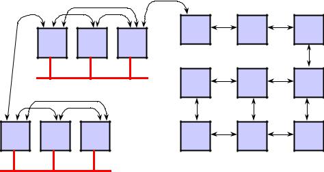
Multiprocessor systems typically use one or both of two methods to communicate between processor nodes. One method uses dedicated point-to-point communication channels. This method is often called data-flow multiprocessing. In the other method, nodes communicate through a single shared global memory via a parallel bus. The SHARC family supports the implementation of point-to-point communication through its six link ports called link port multiprocessing. It also supports an enhanced version of shared parallel bus communication called cluster multiprocessing.
For applications that require high computational bandwidth, but only limited flexibility, data flow multiprocessing is the best solution. The DSP algorithm is partitioned sequentially across several processors and data is passed directly across them as shown on the right side of Figure 7.38. The SHARC is ideally suited for data flow multiprocessing applications because it elminates the need for interprocessor data FIFOs and external memory. Each SHARC has six link ports allowing 2D and 3D arrays as well as traditional data flow. The internal memory of the SHARC is usually large enough to contain both code and data for most applications using this topology. All a data flow system requires are a number of SHARC processors and point-to-point signals connecting them.
7.34
DSP HARDWARE
MULTIPROCESSOR COMMUNICATION
EXAMPLES FOR SHARC
Links |
Links |
Links |
Links |
|
|||
EP |
EP |
EP |
|
SHARC Cluster |
Links |
2D Array
Links |
Links |
Links |
EP |
EP |
Links |
EP |
Dataflow
Links |
Links |
Links |
Links |
Links |
Links |
SHARC Cluster
Expanding Clusters
Link Ports for point-to-point communication
Cluster Bus for high bandwidth parallel communication
On-chip Bus Arbitration
Unified Memory Map
Figure 7.38
EXTERNAL PORT VERSUS
LINK PORT COMMUNICATIONS
Advantages of External Ports (EP)
Communications through the EP has the Highest Bandwidth between two SHARCs (400 Mbytes/s)
Allows up to 6 SHARCs and a Host to share the EP
The EP offers flexible communication of data and control information
The Shared Memory model allows a simple software structure
Advantage of Link Ports
Each Link Port provides independent, 100 MBytes/s communication between two SHARCs
Up to 6 Link Ports (600 MBytes/s)
Easily scalable to any number of SHARCs
Both Link Port and EP communications can be used simultaneously
Figure 7.39
7.35
DSP HARDWARE
Cluster multiprocessing is best suited for applications where a fair amount of flexibility is required. This is especially true when a system must be able to support a variety of different tasks, some of which may be running concurrently. SHARC processors also have an on-chip host interface that allows a cluster to be easily interfaced to a host processor or even to another cluster.
Cluster multiprocessing systems include multiple SHARC processors connected by a parallel bus that allows interprocessor access of on-chip memory as well as access to shared global memory. In a typical cluster of SHARCs, up to six ADSP-21160 processors and a host can arbitrate for the bus. The on-chip bus arbitration logic allows these processors to share the common bus. The SHARC’s other on-chip features help eliminate the need for any extra glue hardware in the cluster multiprocessor configuration. External memory, both local and global, can frequently be eliminated in this type of system.
TIGERSHARC™: THE ADSP-TS001 STATIC
SUPERSCALAR DSP
The ADSP-TS001 is the first DSP from Analog Devices to use the new TigerSHARC™ static superscalar architecture. The TigerSHARC targets telecommunications infrastructure equipment with a new level of integration and the unique ability to process 8-, 16-, 32-bit fixed and floating-point data types on a single chip. Each of these data types is critical to the next generation of telecommunications protocols currently under development, including IMT-2000 (also known as 3G wireless) and xDSL (digital subscriber line). Unlike any other DSP, the ADSP-TS001 has the unique ability to accelerate processing speed based on the data type. Moreover, the chip delivers the highest performance floating-point processing.
In telecommunications infrastructure equipment, voice coder and channel coder protocols are developed around 16-bit data types. To improve signal quality, many telecom applications employ line equalization and echo cancellation techniques that boost overall signal quality and system performance. These algorithms benefit from the added precision of 32-bit and floating-point data processing. The 8-bit native support is well suited to the commonly used Viterbi channel decoder algorithm, as well as image processing where it is more straightforward and cost-effective to represent red, green, and blue components of the signal with 8-bit data types. Many of these applications require high levels of performance and may require algorithms to be executed consecutively or even concurrently. The end application determines the exact requirements. The flexibility of the TigerSHARC architecture enables the software engineer to match the application precision requirements without any loss of system performance. In the TigerSHARC, performance is traded directly against numerical precision.
The TigerSHARC architecture uses key elements from multiple microprocessor types – RISC (reduced instruction set computer), VLIW (very long instruction word), and DSP in order to provide the highest performance digital signal processing engine. The new architecture leverages existing DSP product attributes such as fast and deterministic execution cycles, highly responsive interrupts, and an excellent peripheral interface to support large core computation rates and a high data rate
7.36
DSP HARDWARE
I/O. To achieve excellent core performance, RISC-like features such as load/store operations, a deeply pipelined sequencer with branch prediction, and large interlocked register files are introduced. Additionally, the VLIW (very long instruction word) attributes offer more efficient use of code space, especially for control code.
TigerSHARC®: ANALOG DEVICES’ NEW
STATIC SUPERSCALER DSP ARCHITECTURE
RISC
•Load / store architecture
•Deeply pipelined for high clock rates
•Branch prediction
•Large interlocked register file
VLIW
|
• Instruction level parallelism |
|
determined prior to run time in |
DSP |
multi-instruction lines |
|
•Determinism and real-time execution
•Fast and responsive interrupt system
•I/O and internal memory capable of sustaining core rates
•Fast multiply accumulates, HW support for circular buffers, bit reverse, zero overhead looping
Figure 7.40
TigerSHARC KEY ARCHITECTURAL FEATURES
Core
■1200 MMACs/s @ 150 MHz -- 16-Bit Fixed Point
■300 MMACs/s @150 MHz -- 32-Bit Floating Point
■900 MFLOPS -- 32-Bit Floating Point
Memory
■6 Mbits of on-chip SRAM organized in a unified memory map as opposed to the traditional Harvard architecture.
I/O, Peripherals, & Package
■600 Mbytes/s transfer rate through external bus.
■600 Mbytes/s aggregate transfer rate through 4 Link Ports
■Glueless multiprocessor cluster support for up to 8 ADSP-TS001s
■4 General Purpose I/O Ports
■SDRAM Controller
■360 Ball, SBGA Package 35×35mm
Figure 7.41
7.37
DSP HARDWARE
Finally, to supply all functional blocks with instructions, clever management of the instruction word is necessary. Specifically, multiple instructions must be dispatched to processing units simultaneously, and functional parallelism must be calculated prior to runtime.
By incorporating the best of all worlds, the TigerSHARC architecture will provide a state of the art platform for the most demanding signal processing applications.
The TigerSHARC core shown in Figure 7.42 consists of multiple functional blocks: computation blocks, memory, integer ALUs, and a sequencer. There are two computational blocks (X and Y) in the TigerSHARC architecture, each containing a multiplier, ALU, and 64-bit shifter. With the resources in these blocks, it is possible to execute eight 40-bit MACs on 16-bit data, two 40-bit MACs on 16-bit complex data, or two 80-bit MACs on 32-bit data – all in a single cycle. TigerSHARC is a register-based load/store architecture, where each computational block has access to a fully orthogonal 32-word register file.
ADSP-TS001 TigerSHARC® ARCHITECTURE
|
|
|
|
|
|
|
|
|
|
|
|
|
|
|
|
|
|
|
|
|
|
|
|
|
|
SEQUENCER |
|
|
J ALU |
|
|
|
K ALU |
|
|
|
|||||||||||
|
|
|
|
|
|
|
|
|
0 |
|
|
|
|
|
|
0 |
|
|
|
|
|
|
|
|
|
|
|
|
|
|
|
|
|
|
|
|
|
|
|
|
|
|
|
|
|||
|
|
128-entry |
|
|
|
J-RF |
|
K-RF |
|
|
|
|
|||||||||||
|
|
|
|
|
|
|
|
|
|
|
|
||||||||||||
|
|
BTB |
|
|
|
|
|
|
|
|
|
|
|||||||||||
|
|
|
|
31 |
|
|
|
|
|
|
31 |
|
|
|
|
|
|
|
|||||
|
|
|
|
|
|
|
|
|
|
|
|
|
|
|
|
|
|
|
|
|
EXTERNAL |
||
|
|
|
|
|
|
|
|
|
|
|
|
|
|
|
|
|
|
|
|
|
|
|
|
|
|
|
|
|
|
|
|
|
|
|
|
|
|
|
|
|
|
|
|
|
|
|
|
|
|
|
|
|
|
|
|
|
|
|
|
|
|
|
|
|
|
|
|
|
|
|
|
|
|
128 |
|
|
|
|
|
|
128 |
|
|
|
|
128 |
|
|
|
PORT |
|||||
|
|
|
|
|
|
|
|
|
|
|
|
||||||||||||
128 |
|
|
|
|
|
|
|
|
|
|
|
|
|
|
MD2 |
|
|
|
|
|
|
|
|
|
|
|
|
|
|
|
|
|
|
|
|
|
|
|
|
|
|
|
|
|
|||
128 |
|
|
|
|
|
|
|
|
|
|
|
|
|
MD1 |
|
|
|
|
|
|
DMA |
||
|
|
|
|
|
|
|
|
|
|
|
|
|
|
|
|
|
|
|
|||||
128 |
|
|
|
|
|
|
|
|
|
|
|
|
MD0 |
|
|
|
|
|
|
|
|||
|
|
|
|
|
|
|
|
|
|
|
|
|
|
|
|
|
|
|
|||||
|
|
|
|
|
|
|
|
|
|
|
|
|
|
|
|
|
|
|
|
|
|
|
|
|
|
|
|
|
|
|
|
|
|
|
|
|
|
|
|
|
|
|
|
|
|
|
|
128 |
128 |
128 |
128 |
|
|
PERIPHERALS |
|
128 |
128 |
128 |
|||||
|
|
|
|
||||
Comp Block X |
Comp Block Y |
|
|
|
|||
0 |
ALU |
0 |
ALU |
M0 |
M1 |
M2 |
|
R |
Mult |
R |
Mult |
2Mbit |
2Mbit |
2Mbit |
|
F |
Shift |
F |
Shift |
|
|
|
|
31 |
31 |
ON-CHIP SRAM |
|||||
|
|
|
|
||||
Figure 7.42
7.38
DSP HARDWARE
The TigerSHARC DSP features a short-vector memory architecture organized in three 128-bit wide banks. Quad, long, and normal word accesses move data from the memory banks to the register files for operations. In a given cycle, four 32-bit instruction words can be fetched, and 256 bits of data can be loaded to the register files or stored into memory. Data in 8-, 16-, or 32-bit words can be stored in contiguous, packed memory. Internal and external memories are organized in a unified memory map which leaves specific partitioning to the programmer. The internal memory bandwidth for data and instructions is 7.2 Gbytes/second when operating on a 150MHz clock.
Two integer ALUs are available for data addressing and pointer updates. They support circular buffering and bit reversal, and each has its own 32-word register file. More than simple data address generations units, both integer ALUs support general purpose integer computations. The general purpose nature of the integer ALUs benefits the compiler efficiency and increases programming flexibility.
The TigerSHARC architecture is designated static superscalar, as it executes up to four 32-bit instructions per clock cycle, and the programmer has the flexibility to issue individual instructions to each of the computational units. The sequencer supports predicted execution, where any individual instruction executes according to the result of a previously defined condition. The same instruction can be executed by the two computation blocks concurrently using different data values (this is called SIMD – single-instruction multiple-data operation).
The TigerSHARC architecture enables native operation using 8-, 16-, or 32-bit data values. The overall processor performance increases as the level of data precision decreases.
The inclusion of a branch target buffer (BTB) and static branch prediction logic eliminates the programming task of filling the instruction pipeline after branch instructions. If seen before, the branch is taken in a single cycle.
Three internal 128-bit wide busses ensure a large data bandwidth between internal functional blocks and external peripherals. The three-bus structure matches typical mathematical instructions which require two inputs and compute one output. The programming model is orthogonal and provides for deterministic interrupts.
The TigerSHARC architecture is free of hardware modes. This eliminates wasted cycles and simplifies compiler operation. The instruction set directly supports all DSP, image, and video processing arithmetic types including signed, unsigned, fractional, and integer data types. There is optional saturation (clipping) arithmetic for all cases.
At 150MHz, the ADSP-TS001 offers the highest integer and floating point performance of any SHARC product. Additionally, at 6 Mbits of on-chip SRAM, Analog Devices has increased its level of memory integration by 50% over previous SHARC family members. The migration to smaller process geometries will enable ADI to increase clock frequencies and integrate additional memory for future product derivatives.
7.39
DSP HARDWARE
TigerSHARC KEY FEATURES
Execution of 1 to 4 32-Bit Instructions Per Clock Cycle
Single-Instruction Multiple Data (SIMD) Operations Supported by Two Computation Blocks
Multiple Data Type Computation Blocks
Each With Register File, MAC, ALU, Shifter
32/40-Bit Floating or 32-Bit Fixed Point Operations (6 Per Cycle)
16-Bit (24 Per Cycle) or 8-Bit (32 Per Cycle) Operations
Static Branch Prediction Mechanism, with 128-Entry Branch Target Buffer (BTB)
Internal Bandwidth of 7.2 Gbytes/second
Simple and Fully Interruptible Programming Model
Figure 7.43
The ADSP-TS001 reduces total material costs by integrating multiple I/O and peripheral functions that reduce or eliminate the need for external glue logic and support chips. Specifically, the ADSP-TS001 at 150MHz integrates four glueless link ports with an aggregate transfer rate of 600 Mbytes/s, glueless multiprocessor cluster interface support for up to 8 ADSP-TS001s, an SDRAM controller, and a JTAG controller. This unprecedented functionality is packaged in a 35 by 35mm 360 ball SBGA package.
Typical computation rates and coding details of the TigerSHARC are shown in Figure 7.44. Four 32-bit instructions are executed in parallel forming one 128-bit instruction line. The entire instruction line is executed in one cycle. This example assembly code is for a single line and is performing the following:
xR3:0=Q[j0+=4];// |
load 4 registers (xR0,xR1,xR2,xR3) in the X register file from |
|
|
|
memory |
yR3:0=Q[k0+=4];// |
load 4 registers in the Y register file from memory |
|
FR5=R4*R4; |
// |
multiply 2 32-bit floats in X computational block and |
|
|
2 more in Y (2 multiplies) |
FR9:8=R6+/-R7;;// |
add and subtract in both X and Y computational blocks |
|
|
|
(4 ALU operations) |
7.40
DSP HARDWARE
A single semicolon separates each 32-bit instruction, and a double semicolon indicates the end of an instruction line. This particular example shows the syntax for 32-bit floating point multiplies and ALU operations. Parallel 16-bit operands can easily be specified by using the “S” for “short” prefix instead of the “F” for the “float” prefix. J0 and K0 are IALU registers being used as indirect address pointers for the memory reads.
TigerSHARC PEAK COMPUTATION RATES
■ 4 instructions per cycle accomplishes:
Ö 24 16-bit ops , or 6 32-bit ops Ö 8 16-bit MACs, or 2 32-bit MACs
■As well as 256-bit data moves, and 2 address calculations
|
8 |
16-bit |
16 |
16-bit |
|
|
or |
|
or |
|
|
2 loads carrying 256 bits |
2 |
32-bit |
4 |
32-bit |
|
multiplications |
ALU ops |
||||
2 address calculations |
|||||
in SIMD |
in SIMD |
||||
|
|||||
xR3:0=Q[j0+=4]; yR3:0=Q[k0+=4]; FR5=R4*R4; FR9:8=R6+/-R7;;
Figure 7.44
DSP programmers demand and require the capability to program in both high level languages and low level assembly language. The determination of programming language is dependent upon a number of factors including speed performance, memory size, and time to market considerations. Ultimately, however, the whole DSP product should incorporate features that enable user friendly coding in both high level and low level languages. The TigerSHARC architecture does indeed meet these requirements.
Specifically, the TigerSHARC core includes 128 ea. 32-bit general purpose registers. This large number of registers allows C compilers sufficient flexibility to capitalize on the full potential performance of the architecture. In order to ensure data integrity, all registers are completely interlocked meaning that the programmer does not have to be cognizant of architecture delays. The hardware ensures valid data is used in computations. Additionally, all registers can be accessed via all addressing modes (orthogonal) and a deterministic delay (2 clock cycles) is achieved for all computational instructions. Lastly, the TigerSHARC architecture includes a Branch Target Buffer which holds the effective address of the last 128 branches or jumps. This feature alleviates the programming task of filling the instruction pipeline after branch instructions. If seen before, the architecture jumps to the next instruction in a single clock cycle.
7.41
DSP HARDWARE
ARCHITECTURAL FEATURES FOR HIGH-LEVEL
LANGUAGE SUPPORT
■128 General Purpose Registers
■All Registers Fully Interlocked
■General Purpose Integer ALUs for Addressing
■Branch Prediction
■No Hardware Modes
■Orthogonal Addressing Modes
■Assembly Language Support
Figure 7.45
Figure 7.46 depicts one possible configuration of a TigerSHARC design in a multiprocessing implementation. Up to 8 ADSP-TS001 processors can communicate directly via the high speed 64-bit wide external bus interface. In this type of communication, a commonly used master-slave protocol is implemented which enables any two processors to communicate directly at any one time.
In addition to the primary external bus, a limitless number of processors can be connected via the ADSP-TS001 link ports. While offering more flexibility, link port connectivity provides lower per port bandwidth than the primary external bus interface. Again, all data transfers via the link ports are managed by a dedicated I/O processor and require no CPU intervention.
To summarize, the data I/O bandwidth of the link port (600MBytes/s) and external port (600MBytes/s) can be aggregated yielding an overall individual processor data bandwidth of 1200 Mbytes/s with 150MHz clock operation. Additionally, both the link port interface and the multiprocessor cluster interface are both completely glueless.
The ADSP-TS001 is the first member of a planned family of TigerSHARC-based products. Specifically, future members of the TigerSHARC family will contain optimized mixes of memory and peripherals to meet the requirements of specific target markets. These markets include third generation cellular base stations and VOIP (Voice Over the Internet Protocol) servers/concentrators. Additionally, process and design improvements will double the baseline performance of the general purpose TigerSHARC family members.
7.42
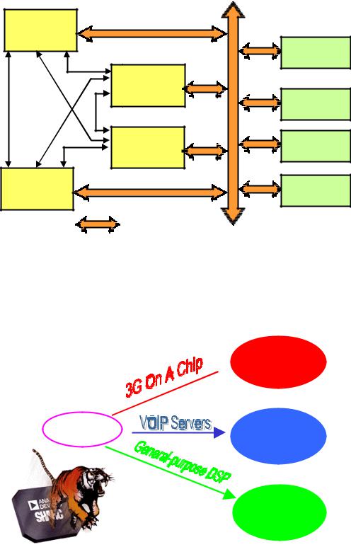
DSP HARDWARE
MULTIPROCESSING COMMUNICATION VIA LINK PORTS AND CLUSTER BUS
ADSP-TS001
TigerSHARC
Link Port connections
ADSP-TS001
TigerSHARC
ADSP-TS001 |
TigerSHARC |
ADSP-TS001
TigerSHARC
SRAM
DRAM
SDRAM
I/O
Host Interface
Bus connections
Figure 7.46
TigerSHARC ROADMAP
250 MHz
2 Mbit/sec  channel on a chip
150 MHz
ADSP-TS001 |
Highest Density |
|
Voice Over |
||
|
||
|
The Internet |
2.4 Billion
MACs per
Second
Figure 7.47
7.43
DSP HARDWARE
Comparing DSPs based solely on MIPS, MOPS, or MFLOPS does not tell the entire performance story. It is much more useful to compare DSPs based on their performance with respect to specific algorithms. The FFT and the FIR filter are popular benchmarks as well as the IIR biquad filter, matrix multiplications, division, and square root.
Figure 7.48 shows the benchmark performance of the ADSP-TS001 TigerSHARC operating on 16-bit fixed point data. Figure 7.49 shows its benchmark performance operating on 32-bit floating point data.
ADSP-TS001 TigerSHARC BENCHMARKS @ 150MHz
16-BIT PERFORMANCE
■ 16-Bit performance -- 1200 MMACs/s peak performance
Algorithm |
Execution |
Cycles to |
|
Time |
|
Execute |
|
|
|
|
|
256 Point Complex FFT (Radix 2) |
7.3 |
µs |
1100 |
50 Tap FIR on 1024 inputs |
48 |
µs |
7200 |
Single FIR MAC |
0.93 ns |
0.14 |
|
Single Complex FIR MAC |
3.80 ns |
0.57 |
|
Single FFT Butterfly |
6.7 ns |
1.0 |
|
|
|
|
|
Figure 7.48 |
|
|
|
ADSP-TS001 TigerSHARC BENCHMARKS @ 150MHz
32-BIT PERFORMANCE
■ 32-Bit performance -- 300 MMACs/s peak performance
|
Algorithm |
Execution |
Cycles to |
|
|
Time |
Execute |
||
|
|
|
|
|
|
1024 Point Complex FFT (Radix 2) |
69 µs |
10300 |
|
|
50 Tap FIR on 1024 Input |
184 µs |
27500 |
|
|
Single FIR MAC |
3.7 ns |
0.55 |
|
|
Single FFT Butterfly |
13.3 ns |
2.0 |
|
|
Single Complex FIR MAC |
13.3 ns |
2.0 |
|
|
|
|
|
|
|
Divide |
20 ns |
3.0 |
|
|
|
|
|
|
|
Square Root |
33.3 ns |
5.0 |
|
|
Viterbi Decode(per Add/Compare/Select) |
3.3 ns |
0.5 |
|
|
|
|
|
|
Figure 7.49
7.44
DSP HARDWARE
DSP EVALUATION AND DEVELOPMENT TOOLS
The availability of a complete set of hardware and software development tools is essential to any DSP-based design. A typical DSP system design cycle is described below.
The first step in the process is to describe the system architecture. This would include such things as the type of processor, the peripherals (external memory, codecs, host processor, links), the configuration, etc. This information is placed in a file known as the Link Descriptor File (or LDF).
The next step in the process is to generate the actual DSP code. This can be done using a higher level language (usually C or C++), the DSP assembly language, or a combination of both. DSP code developed in C must be compiled and assembled in order to generate the assembly language code. While programming in C is easier, the resulting assembly code which results after compiling is not as efficient as if the coding had been done in assembly language originally. For this reason, many DSP programmers do most of the programming in C, but use assembly language for the critical loops in the program. The Analog Devices’ DSP assembly language is based on algebraic syntax and is relatively easy to use directly. The linker then generates an executable file.
The software must then be debugged using the software simulator in conjunction with an evaluation board such as the EZ-LAB evaluation board or perhaps a thirdparty card which plugs into a slot in the PC.
After the software is debugged using the evaluation board, it must be tested with the actual system target board (this is the board that you design with the DSP in your system). An in-circuit emulator, such as the EZ-ICE, interfaces with the target board, usually via a PCI or a JTAG interface port and connector.
The final step in the process is to generate the code required for booting the system using the prom splitter.
A summary of the tools available from Analog Devices is shown in Figure 7.50. Each one will be discussed in detail.
EZ-KIT Lites are basically DSP starter kit evaluation boards. In addition to the processor itself, these boards contain an ADC and a DAC (codec) which interfaces to the DSP over the DSP serial port. All necessary analog and digital support circuitry is contained on the boards. The options on the board are controlled over an RS-232 port connection to a PC as well as jumpers on the board. Windows 95/98/NT compatible software is supplied with the board. The software includes limited code generation tools including a limited feature set compiler, assembler, linker, prom splitter (loader), and Visual DSP debugger. Application examples such as DTMF generator, echo cancellation, FFT, simple digital filters, etc., are included as part of the software. The EZ-KIT Lite boards are primarily starter kit evaluation systems (and “lite” on the wallet!).
7.45
DSP HARDWARE
ADI DSP DEVELOPMENT TOOLS
■EZ-KIT Lite Evaluation Boards
■Emulators
■Integrated Development Environment (IDE) Software, VisualDSP® and VisualDSP++
Assembler, Linker, PROM Splitter, HIP Splitter, Simulator, Compiler, Debugger
■Extensive Algorithm Libraries
■Factory, Field, and WWW Support
■Seminars
■ADI and Third Party DSP Workshops
■ADI DSP Collaborative™ Third Party Support
Figure 7.50
EZ-KIT LITE’S™ FOR ANALOG DEVICES’ DSPS
■The EZ-KIT Lite is a stand-alone (desktop) system that connects to a PC running on Windows
■The EZ-KIT Lites provide:
A cost effective method for initial evaluation of the capabilities of ADSP-series DSPs.
A powerful development environment for a variety of general purpose applications.
■Target market:
First time DSP users
First time ADI DSP users
Existing ADI DSP users implementing new designs
Existing ADI DSP users upgrading to faster devices for current designs
Figure 7.51
7.46

DSP HARDWARE
ADSP-2189M EZ-KIT LITE™
■Hardware Features
ADSP-2189M 75 Mips processor
AD73322L Stereo codec
DSP-programmable CODEC gain
2 Mbit or greater boot protected Flash EPROM.
RS-232 PC to EZ-Kit Lite interface
Selectable Host vs. Full Memory mode implemented via dip switch
ADSP-218x EZ-ICE emulator port connector
Expansion connector includes all signal I/O plus 5V, 3.3V, 2.5V, and GND connections
LED indicators for master power, RS-232 interface, and one PF I/O
■Software Features
Windows 95/98/NT-4.0 PC host support
VisualDSP : Limited feature set compiler, assembler, linker, prom splitter (loader), VisualDSP debugger interface
Application Examples: DTMF Generator, Echo Cancellation, FFT, etc.(similar to 2181 EZ-KIT Lite)
Email Support
Figure 7.52
ADSP-21160M EZ-KIT LITE™
■Hardware Features
ADSP-21160M SHARC processor
AD1881 16-bit Stereo AC’97 SoundMAX Codec
EPROM flash memory (2 Mbit)
JTAG header
Support for ADSP-2116x family of processors
64K x 64 bit SBSRAM
Enhanced parallel port
CE compliant
■Software Features
Support for Win95, Win98 and WinNT
Evaluation suite of VisualDSP++ : compiler, assembler, linker, prom splitter (loader), VisualDSP debugger interface. VisualDSP limited to use with EZ-KIT Lite hardware
DEMONSTRATIONS: DFT.dxe, BP.dxe, Pluck.dxe, Primes.dxe, Tt.dxe
Figure 7.53
7.47
DSP HARDWARE
ADSP-21065L EZ-KIT LITE™
Hardware Features
ADSP-21065L SHARC DSP running at 60MHz
Full Duplex, 16-Bit Audio Codec
RS-232 Interface with UART
JTAG Emulation Connector
Expansion via MAFE+ Connector
Software Features
Support for Win95, Win98 and WinNT
Evaluation suite of VisualDSP++ : compiler, assembler, linker, prom splitter (loader), VisualDSP debugger interface. VisualDSP limited to use with EZ-KIT Lite hardware
Demonstrations: Fast Fourier Transform (FFT), Discrete Fourier Transform (DFT), Band Pass Filter, Pluck String Themes, Talk Through
Figure 7.54
The final step in the DSP system development is the debugging of the actual system, or “target” board. The Analog Devices’ in-circuit emulator, EZ-ICE, interfaces with a connector on the target board for use in final system hardware and software debugging. Examples are shown in Figures 7.55 through 7.58. Figure 7.56 shows the Apex-ICE which interfaces to the target board via a JTAG connector which in turn interfaces to the SHARC DSP. A USB port connector is used to interface the emulator to a PC. Other in-circuit emulators are available which interface to ISA, PCI, RS232, and Ethernet ports.
7.48
DSP HARDWARE
EZ-ICE® FOR THE ADSP-218x DSP FAMILY
■Serial port interface, printed circuit board and 14-pin header
■Controls equipment for testing, observing, and debugging a target system
■6 foot cable
■Hardware switch to accommodate of 2.5V, 3.3V, and 5V
■Shielded enclosure to cover bare circuit board
■Performance increase via faster data transfer
Figure 7.55
APEX-ICE™ USB EMULATOR
■Universal Serial Bus (USB)- based emulator for Analog Devices JTAG DSPs
■First portable solution for Analog Devices JTAG DSPs
■Small hand-held unit
■Small diameter cable, 5 meters in length, for hard to reach targets
■Power provided externally
JTAG CONNECTOR
USB PORT
CONNECTOR
Figure 7.56
7.49
DSP HARDWARE
TREK-ICE™ ETHERNET EMULATOR
■Network hosted mini-tower emulator with 10-Base-T port
■Installs to a LAN as easy as a laser printer
■Remote debugging between either PC or SUN workstation debug host (client) and the target DSP system
■Rugged high-speed 3V/5V pod
■Flexible emulator cable (1.5m)
Figure 7.57
SUMMIT-ICE™ PCI EMULATOR
■32-bit PCI interface add-in card
■Four inch, flexible shielded target board cable for easy access to a 14-pin JTAG header
■Embedded ICEPAC technology provides a rugged and reliable solution
■Remote 3V/5V JTAG Pod with extended, shielded cable (1.5 m)
■Windows 95 & NT PNP
Figure 7.58
7.50
DSP HARDWARE
VISUALDSP® AND VISUALDSP++
New development software for Analog Devices’ DSPs is written in easy to use VisualDSP® and VisualDSP ++ which is Windows 95/98/NT compatible. VisualDSP is a completely integrated development environment which uses an algebraic syntax assembler and an optimized C compiler. Multiprocessor environments can be simulated and debugged as well. VisualDSP++ provides C++ language support.
VisualDSP versions currently exist for the ADSP-218x and ADSP-219x families as well as the SHARC family of DSPs.
A “test drive” CDROM is available with a limited license for evaluation purposes.
In addition to the tools and support functions described thus far, Analog Devices’ DSP Collaborative consists of over 80 companies who provide a range of products and services to make the DSP design task easier. Over 30 companies support the 16-bit ADSP-21xx family, and over 50 companies support the SHARC DSP family. A directory of the collaborative can be found at:
http://www.analog.com/industry/dsp/3rdparty/index.html
Further information about Analog Devices’ DSP tools can be found at:
http://www.analog.com/dsp/tools
SOFTWARE DEVELOPMENT ENVIRONMENT
VisualDSP® and VisualDSP++
Debugger front-end
Integrated development environment (IDE)
Algebraic syntax assembler
Cycle-accurate instruction level simulator
Optimizing ANSI C compiler with inline assembly
Math, DSP, and C runtime libraries
Sophisticated multiprocessor linker
Intelligent loader
ADSP-218x, 219x: Windows 95, 98, NT, 2000 Compatible
SHARC: Windows 95, 98, NT, 2000 Compatible
Figure 7.59
7.51
DSP HARDWARE
VisualDSP® 7.0 FOR ADSP-218x AND ADSP-219x
■Hosted on Windows 95, Windows 98, Windows NT 4.0 with SP3 or later
■ADSP-219x simulator target supports the 219x core
■ELF/DWARF toolset, including compiler with classical and processor-specific optimizations
■Tcl command line scripting language
Support automated test of DSP system
■21xx Object Translator
■Peripheral Code Wizard supporting 218x and 219x peripherals
Figure 7.60
VisualDSP++™ FOR SHARC® DSPs
■Supports Windows 95, 98, NT, 2000
■ELF/Dwarf-2 file format enables effective debug operation
■Pre-processor for linker/assembler separate from compiler
■Fast ICE stepping - 0.9 sec. per step
■MultiProcessor (MP) support
Synchronous run, step, and halt
■Tcl command line scripting language
Support automated test of DSP system
■Statistical Profiling
■C++ capabilities
■Graphical Plotting
Figure 7.61
7.52
DSP HARDWARE
TigerSHARC® DEVELOPMENT TOOLS
■The TigerSHARC architecture is supported by a robust set of simulation, code generation, and debug tools that includes:
VisualDSP Integrated Development Environment
●Simulator, Assembler, Loader, Debugger, and Compiler
●DSP & Math Libraries
Emulators – All present ADI JTAG emulators support the TigerSHARC DSP family
EZ-KIT Lite
■Successive VisualDSP revisions will continuously increase functionality.
Figure 7.62
VisualDSP TEST DRIVE
■The test drive is a 30-day evaluation of VisualDSP's full package. It does not include a tutorial. The new test drive is a full version of VisualDSP and contains pdf.'s of the VisualDSP manuals.
■The customer is presented with the test drive CD. The customer than proceeds to the Analog Devices DSP Tools website, clicks on Test Drive Registration www.analog.com/industry/dsp/tools/test_drive.html and registers online. After they complete the registration process they will receive a serial number immediately that will allow them to use the test drive. The test drive will expire 30-days from the install and they will not be able to register the test drive again.
■The SHARC VisualDSP test drive is now available, SAP part # VDSP-SHARC-PC-TEST.
■The VisualDSP TigerSHARC test drive will be available Summer 2000
■The VisualDSP ADSP-218x/219x test drive will be available in September 2000
Figure 7.63
7.53
DSP HARDWARE
ADI DSP COLLABORATIVE - WHAT IS IT?
Over 80 Companies that provide a wide range of products and services to make your design challenge easier
Architecture Coverage
Over 30 Companies support 16-bit, ADSP-21xx Family
Over 50 Companies support SHARC® DSP Family
Over 400 Products from the Following Categories:
Algorithms |
Emulators |
Real-Time Operating Systems |
Hardware Development Boards |
Debuggers |
Graphical S/W Programs |
MATLAB® DSP Support |
Consulting Services |
Focused Applications : |
|
Audio |
Motor/Motion Control |
Digital Radio |
Radar/Sonar |
Industrial Inspection & Control |
Telecom |
Medical Instrumentation/Imaging Video/Sound Processing
Military/Aerospace
■http://www.analog.com/industry/dsp/3rdparty/index.html
Figure 7.64
7.54
DSP HARDWARE
REFERENCES
1.Steven W. Smith, The Scientist and Engineer’s Guide to Digital Signal Processing, Second Edition, 1999, California Technical Publishing,
P.O. Box 502407, San Diego, CA 92150. Also available for free download at: http://www.dspguide.com or http://www.analog.com/industry/dsp/dsp_book
2.C. Britton Rorabaugh, DSP Primer, McGraw-Hill, 1999.
3.Richard J. Higgins, Digital Signal Processing in VLSI, Prentice-Hall, 1990.
4.Ethan Bordeaux, Advanced DSP Performance Complicates Memory Architecures in Wireless Designs, Wireless Systems Design, April 2000.
5.DSP Designer’s Reference (DSP Solutions) CDROM, Analog Devices, 1999.
6.DSP Navigators: Interactive Tutorials about Analog Devices’ DSP Architectures (Available for ADSP-218x family and SHARC family): http://www.analog.com/industry/dsp/training/index.html#Navigator
7.General DSP Training and Workshops: http://www.analog.com/industry/dsp/training
The following DSP Reference Manuals and documentation are available for free download from: http://www.analog.com/industry/dsp/tech_docs.html
8.ADSP-2100 Family Users Manual, 3rd Edition, Sept., 1995.
9.ADSP-2100 Family EZ Tools Manual.
10.ADSP-2100 EZ-KIT Lite Reference Manual.
11.Using the ADSP-2100 Family, Vol. 1, Vol. 2.
12.ADSP-2106x SHARC User’s Manual, 2nd Edition, July, 1996.
13.ADSP-2106x SHARC EZ-KIT Lite Manual.
14.ADSP-21065L SHARC User’s Manual, Sept. 1, 1998.
15.ADSP-21065L SHARC EZ-LAB User’s Manual.
16.ADSP-21160 SHARC DSP Hardware Reference.
7.55
DSP HARDWARE
7.56