

ЦОС_Заочники2013 / Книги по ЦОС / Дополнительная литература / Основы ЦОС (на англ.яз) / MS10
.pdfHARDWARE DESIGN TECHNIQUES
SECTION 10
HARDWARE DESIGN TECHNIQUES
■Low Voltage Interfaces
■Grounding in Mixed Signal Systems
■Digital Isolation Techniques
■Power Supply Noise Reduction and Filtering
■Dealing with High Speed Logic
10.a
HARDWARE DESIGN TECHNIQUES
10.b
HARDWARE DESIGN TECHNIQUES
SECTION 10
HARDWARE DESIGN TECHNIQUES
Walt Kester
LOW VOLTAGE INTERFACES
Ethan Bordeaux, Johannes Horvath, Walt Kester
For the past 30 years, the standard VDD for digital circuits has been 5V. This voltage level was used because bipolar transistor technology required 5V to allow headroom for proper operation. However, in the late 1980s, Complimentary Metal Oxide Semiconductor (CMOS) became the standard for digital IC design. This process did not necessarily require the same voltage levels as TTL circuits, but the industry adopted the 5V TTL standard logic threshold levels to maintain backward compatibility with older systems (Reference 1).
The current revolution in supply voltage reduction has been driven by demand for faster and smaller products at lower costs. This push has caused silicon geometries to drop from 2µm in the early 1980s to 0.25µm that is used in today’s latest microprocessor and IC designs. As feature sizes have become increasingly smaller, the voltage for optimum device performance has also dropped below the 5V level. This is illustrated in the current microprocessors for PCs, where the optimum core operating voltage is programmed externally using voltage identification (VID) pins, and can be as low as 1.3V.
The strong interest in lower voltage DSPs is clearly visible in the shifting sales percentages for 5V and 3.3V parts. Sales growth for 3.3V DSPs has increased at more than twice the rate of the rest of the DSP market (30% for all DSPs versus more than 70% for 3.3V devices). This trend will continue as the high volume/high growth portable markets demand signal processors that contain all of the traits of the lower voltage DSPs.
On the one hand, the lower voltage ICs operate at lower power, allow smaller chip areas, and higher speeds. On the other hand, the lower voltage ICs must often interface to other ICs which operate at larger VDD supply voltages thereby causing interface compatibility problems. Although lower operating voltages mean smaller signal swings, and hence less switching noise, noise margins are lower for low supply voltage ICs.
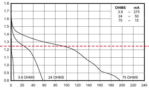
The popularity of 2.5V devices can be partially explained by their ability to operate from two AA alkaline cells. Figure 10.2 shows the typical discharge characteristics for a AA cell under various load conditions (Reference 2). Note that at a load current of 15mA, the voltage remains above +1.25V (2.5V for two cells in series) for nearly 100 hours. Therefore, an IC that can operate effectively at low currents with a supply voltage of 2.5V ±10% (2.25V - 2.75V) is very useful in portable designs. Also, DSPs that have low mA/MIPS ratings and can integrate peripherals onto a single chip, such as the ADSP-218x L or M-series, are useful in portable applications.
10.1
HARDWARE DESIGN TECHNIQUES
LOW VOLTAGE MIXED-SIGNAL ICs
■Lower Power for Portable Applications
■2.5V ICs Can Operate on Two “AA” Alkaline Cells
■Faster CMOS Processes, Smaller Geometries, Lower Breakdown Voltages
■Multiple Voltages in System: +5V, +3.3V, +2.5V, +1.8V DSP Core Voltage (VID), Analog Supply Voltage
■Interfaces Required Between Multiple Logic Types
■Lower Voltage Swings Produce Less Switching Noise
■Lower Noise Margins
■Less Headroom in Analog Circuits Decreases Signal Swings and Increases Sensitivity to Noise (But that’s the subject of an entire seminar!)
Figure 10.1
DURACELL MN1500 “AA” ALKALINE BATTERY
DISCHARGE CHARACTERISTICS
VOLTAGE
(V)
1.25
SERVICE HOURS
Courtesy: Duracell, Inc., Berkshire Corporate Park, Bethel, CT 06801
http://www.duracell.com
Figure 10.2
10.2
HARDWARE DESIGN TECHNIQUES
In order to understand the compatibility issues relating to interfacing ICs operated at different VDD supplies, it is useful to first look at the structure of a typical CMOS logic stage as shown in Figure 10.3.
TYPICAL CMOS IC OUTPUT DRIVER CONFIGURATION
VDD |
|
|
VDD |
|
|
|
|
|
VDD |
High = “1” |
|
VDD |
|
|
|
|
|
|
|
|
|
||||||
|
High = “1” |
|
|
|
|
|
|
PMOS |
|
||||
|
|
|
|
|
|
|
|
||||||
VIH MIN |
|
PREDRIVER |
|
|
|
|
|
|
VOH MIN |
||||
|
|
|
|
|
|
|
|||||||
|
|
|
|
|
|
|
|
|
|
||||
|
|
|
|
|
|
|
|
|
|||||
|
INPUT |
|
|
|
|
|
|
|
OUTPUT |
|
|||
|
|
|
|
|
|
|
|
|
|
||||
|
|
|
|
|
|
|
|
|
|||||
|
|
LOGIC |
|
|
|
|
|
|
|
|
|
||
VIL MAX |
|
Low = “0” |
|
|
|
|
|
|
NMOS |
Low = “0” |
|
VOL MAX |
|
|
|
|
|
|
|
|
|
||||||
|
|
|
|
|
|
|
|
||||||
|
|
|
|
|
|
|
|
|
|
||||
0V |
|
|
|
|
|
|
|
|
|
|
|||
|
|
|
|
|
|
|
|
|
|
||||
|
|
|
|
|
|
|
|
|
|
|
0V |
||
|
|
|
|
|
|
|
|
|
|
|
|
||
VIL MAX = Maximum Allowable Input Low Logic Level
VIH MIN = Minimum Allowable Input High Logic Level
VOL MAX = Maximum Allowable Output Low Logic Level
VOH MIN = Minimum Allowable Output High Logic Level
Figure 10.3
Note that the output driver stage consists of a PMOS and an NMOS transistor. When the output is high, the PMOS transistor connects the output to the +VDD supply through its low on-resistance (RON), and the NMOS transistor is off. When the output is low, the NMOS transistor connects the output to ground through its on-resistance, and the PMOS transistor is off. The RON of a CMOS output stage can vary between 5Ω and 50Ω depending on the size of the transistors, which in turn, determines the output current drive capability.
A typical logic IC has its power supplies and grounds separated between the output drivers and the rest of the circuitry (including the pre-driver). This is done to maintain a clean power supply, which reduces the effect of noise and ground bounce on the I/O levels. This is increasingly important, since added tolerance and compliance are critical in I/O driver specifications, especially at low voltages.
Figure 10.3 also shows “bars” which define the minimum and maximum required input and output voltages to produce a valid high or low logic level. Note that for CMOS logic, the actual output logic levels are determined by the drive current and the RON of the transistors. For light loads, the output logic levels are very close to 0V and +VDD. The input logic thresholds, on the other hand, are determined by the input circuit of the IC.
There are three sections in the “input” bar. The bottom section shows the input range that is interpreted as a logic low. In the case of 5V TTL, this range would be
10.3
HARDWARE DESIGN TECHNIQUES
between 0V and 0.8V. The middle section shows the input voltage range where it is interpreted as neither a logic low nor a logic high. The upper section shows where an input is interpreted as a logic high. In the case of 5V TTL, this would be between 2V and 5V.
Similarly, there are three sections in the “output” bar. The bottom range shows the allowable voltage for a logic low output. In the case of 5V TTL, the IC must output a voltage between 0V and 0.4V. The middle section shows the voltage range that is not a valid high or low - the device should never transmit a voltage level in this region except when transitioning from one level to the other. The upper section shows the allowable voltage range for a logic high output signal. For 5V TTL, this voltage is between 2.4V and 5V. The chart does not reflect a 10% overshoot/undershoot also allowed on the inputs of the logic standard.
A summary of the existing logic standards using these definitions is shown in Figure 10.4. Note that the input thresholds of classic CMOS logic (series-4000, for example) are defined as 0.3VDD and 0.7VDD. However, most CMOS logic circuits in use today are compatible with TTL and LVTTL levels which are the dominant 5V and 3.3V operating standards for DSPs. Note that 5V TTL and 3.3V LVTTL input and output threshold voltages are identical. The difference is the upper range for the allowable high levels.
LOW VOLTAGE LOGIC LEVEL STANDARDS
VOLTS |
5V CMOS |
|
5V TTL |
|
|
|
|
|
|
|
|
||
5.0 |
|
|
|
|
|
|
|
I = INPUT |
|
|
|
|
|
4.5 |
|
|
|
|
|
|
|
|
|
|
|
|
|
I |
|
O |
I |
O |
|
O = OUTPUT |
|
|
|
|
|||
4.0 |
|
|
|
|
|
|
|||||||
|
|
|
|
|
|
3.3V LVTTL |
2.5V VCX |
|
|
||||
3.5 |
|
|
|
|
|
|
|
|
|||||
|
|
|
|
|
|
|
|
|
|
|
|
|
|
3.0 |
|
|
|
|
|
|
I |
O |
|
|
|
2.5V JEDEC |
|
|
|
|
|
|
|
|
|
|
|
|
|
||
2.5 |
|
|
|
|
|
|
|
|
I |
|
O |
I |
O |
2.0 |
|
|
|
|
|
|
|
|
|
||||
|
|
|
|
|
|
|
|
|
|
|
|
|
|
1.5 |
|
|
|
|
|
|
|
|
|
|
|
|
|
1.0 |
|
|
|
|
|
|
|
|
|
|
|
|
|
0.5 |
|
|
|
|
|
|
|
|
|
|
|
|
|
0 |
5V CMOS input |
5V CMOS output |
|
5V TTL input |
5V TTL output |
|
3.3V LVTTL input |
3.3V LVTTL output (-2mA) |
2.5V VCX input |
2.5V VCX output |
|
2.5V JEDEC input |
2.5V JEDEC output (-1mA) |
|
(20uA) |
(-2mA) |
(-12mA) |
||||||||||
Figure 10.4
10.4
HARDWARE DESIGN TECHNIQUES
The international standards bureau JEDEC (Joint Electron Device Engineering Council) has created a 2.5V standard (JEDEC standard 8-5) which will most likely become the minimum requirement for 2.5V operation (Reference 3). However, there is no current (2000) dominant 2.5V standard for IC transmission and reception, because few manufacturers are making products that operate at this voltage. There is one proposed 2.5V standard created by a consortium of IC manufacturers, titled the Low Voltage Logic Alliance. Their specification provides a guideline for semiconductor operation between 1.8V and 3.6V. A standard covering this voltage range is useful because it ensures present and future compatibility. As an example, the 74VCX164245, a bus translator/transceiver from Fairchild Semiconductor, is designed to be operated anywhere between 1.8V - 3.6V and has different input and output characteristics depending upon the supplied VDD. This standard, named VCX, was formed by Motorola, Toshiba and Fairchild Semiconductor. It currently consists primarily of bus transceivers, translators, FIFOs and other building block logic. There are also a wide range of other low voltage standards, such as GTL (Gunning Transceiver Logic), BTL (Backplane Transceiver Logic), and PECL (PseudoECL Logic). However, most of these standards are aimed at application specific markets and not for general purpose semiconductor systems.
The VCX devices can be operated on a very wide range of voltage levels (1.8V - 3.6V). The I/O characteristics of this standard are dependent upon the VDD voltage and the load on each pin. In Figure 10.4, one voltage (2.5V) was chosen to show the general I/O behavior of a VCX device. Each of the device’s output voltages is listed for a specific current. As the current requirements increase, the output high voltage decreases while the output low voltage increases. Please refer to the appropriate data sheets for more specific I/O information.
From this chart, it is possible to visualize some of the possible problems in connecting together two ICs operating on different standards. One example would be connecting a 5V CMOS device to a 3.3V LVTTL IC. The 5V CMOS high level is too high for the LVTTL to handle ( > 3.3V). This could cause permanent damage to the LVTTL chip. Another possible problem would be a system with a 2.5V JEDEC IC driving a 5V CMOS device. The logic high level from the 2.5V device is not high enough for it to register as a logic high on the 5V CMOS input (VIH MIN = 3.5V). These examples illustrate two possible types of logic level incompatibilities - either a device being driven with too high a voltage or a device not driving a voltage high enough for it to register a valid high logic level with the receiving IC. These interfacing problems introduce two important concepts: voltage tolerance and voltage compliance.
VOLTAGE TOLERANCE AND VOLTAGE COMPLIANCE
A device that is voltage tolerant can withstand a voltage greater than its VDD on its I/O pins. For example, if a device has a VDD of 2.5V and can accept inputs equal to 3.3V and can withstand 3.3V on its outputs, the 2.5V device is called 3.3V tolerant. The meaning of input voltage tolerance is fairly obvious, but the meaning of output voltage tolerance requires some explanation. The output of a 2.5V CMOS driver in the high state appears like a small resistor (RON of the PMOS FET) connected to 2.5V. Obviously, connecting its output directly to 3.3V is likely to destroy the device due to excessive current. However, if the 2.5V device has a three-state output which is connected to a bus which is also driven by a 3.3V IC, then the meaning becomes
10.5
HARDWARE DESIGN TECHNIQUES
clearer. Even though the 2.5V IC is in the off (third-state) condition, the 3.3V IC can drive the bus voltage higher than 2.5V, potentially causing damage to the 2.5V IC output.
A device which is voltage compliant can receive signals from and transmit signals to a device which is operated at a voltage greater than its own VDD. For example, if a device has a 2.5V VDD and can transmit and receive signals to and from a 3.3V device, the 2.5V device is said to be 3.3V compliant.
The interface between the 5V CMOS and 3.3V LVTTL parts illustrates a lack of voltage tolerance; the LVTTL IC input is overdriven by the 5V CMOS device output. The interface between the 2.5V JEDEC and the 5V CMOS part demonstrates a lack of voltage compliance; the output high level of the JEDEC IC does not comply to the input level requirement of a the 5V CMOS device.
LOGIC VOLTAGE TOLERANCE
AND COMPATIBILITY DEFINITIONS
Voltage Tolerance:
A device that is Voltage Tolerant can withstand a voltage
greater than its VDD on its input and output pins. If a device has a VDD of 2.5V and can accept inputs of 3.3V (±10%), the 2.5V device is 3.3V tolerant on its input. Input and output tolerance should be examined and specified separately.
Voltage Compliance:
A device that is Voltage Compliant can transmit and receive signals to and from logic which is operated at a voltage
greater than its own VDD. If a device has a 2.5V VDD and can properly transmit signals to and from 3.3V logic, the 2.5V device is 3.3V compliant. Input and output compliance should be examined and specified separately.
Figure 10.5
INTERFACING 5V TO 3.3V SYSTEMS USING NMOS FET BUS
SWITCHES
When combining ICs that operate on different voltage standards, one is often forced to add additional discrete elements to ensure voltage tolerance and compliance. In order to achieve voltage tolerance between 5V and 3.3V logic, for instance, a bus switch voltage translator, or QuickSwitch™ can be used (Reference 4, 5). The bus switch limits the voltage applied to an IC. This is done to avoid applying a larger input high voltage than the receiving device can tolerate.
As an example, it is possible to place a bus switch between a 5V CMOS and 3.3V LVTTL IC, and the two devices can then transmit data properly as shown in Figure 10.6. The bus switch is basically an NMOS FET. If 4.3V is placed on the gate of the FET, the maximum passable signal is 3.3V (approximately 1V less than the gate
10.6
HARDWARE DESIGN TECHNIQUES
voltage). If both input and output are below 3.3V, the NMOS FET acts as a low resistance (RON ≈ 5Ω). As the input approaches 3.3V, the FET on-resistance increases, thereby limiting the signal output. The QuickSwitch contains 10 bidirectional FETs with a gate drive enable as shown in Figure 10.6. The VCC of the QuickSwitch sets the high level for the gate drive.
One way of creating a 4.3V supply on a 5V/3.3V system board is to place a diode between the 5V supply and VCC on the QuickSwitch. In Figure 10.6, the 4.3V is generated by a silicon diode in series with a Schottky diode connected to the 3.3V supply. With 10% tolerances on both 5V and 3.3V supplies, this method produces a more stable gate bias voltage. Some bus switches are designed to operate on either 3.3V or 5V directly and generate the internal gate bias level internally.
A QuickSwitch removes voltage tolerance concerns in this mixed logic design. One convenient feature of bus switches is that they are bi-directional; this allows the designer to place a bus translator between two ICs and not have to create additional routing logic for input and output signals.
+3.3V / +5V BIDIRECTIONAL INTERFACE USING NMOS FET ACHIEVES VOLTAGE TOLERANCE
+ 3.3V BUS |
≈ 1V |
+ 5V BUS |
|
470 kΩ |
|
|
+ 4.3V |
|
Si |
SCHOTTKY |
|
|
0.1µF |
|
3.3V ± 10% |
|
5V ± 10% |
LOGIC |
NMOS |
LOGIC |
|
|
|
|
RON = 5 Ω |
|
“1” = DISABLE |
0V / VCC |
|
|
|
|
“0” = ENABLE |
|
QS3384 QuickSwitch ® |
|
|
10 SWITCHES/PACKAGE |
OPERATE WITH QS3384 VCC = +4.3V
Figure 10.6
A bus switch increases the total power dissipation along with the total area required to layout a system. Since voltage bus switches are typically CMOS circuits, they have very low power dissipation ratings. An average value for added continuous power dissipation is 5mW per package (10 switches), and this is independent of the frequency of signals which pass through the circuit. Bus switches typically have 8 - 20 I/O pins per package and take up approximately 25 to 50mm2 of board space.
10.7
HARDWARE DESIGN TECHNIQUES
One concern when adding interface logic into a circuit is a possible increase in propagation delay. Added propagation delay can create many timing problems in a design. QuickSwitches have very low propagation delay values (< 0.25ns) as shown in Figure 10.7.
QS3384 QuickSwitch® TRANSIENT RESPONSE
WITH +4.3V SUPPLY
VIN
VOUT
(VOLTS)
2.0V
0.8V
|
|
|
|
|
|
|
|
|
|
|
|
|
|
|
|
|
|
|
|
|
|
|
|
|
|
|
|
|
|
|
|
|
|
|
5V TTL, |
|
|
|
|
|
|
|
|
|
|
|
|
|
|
|
|
|
|
|
|
|
|
|
|
|
|
|
|
||||||
3.3V LVTTL |
|
|
|
|
|
|
|
|
TIME (ns) |
|
|
|
|
|
|
|
|
|
|
|
|
|
|
|||||||||||
INPUT THRESHOLDS |
|
|
|
|
|
|
|
|
|
|
|
|
|
|
|
|
|
|
|
|
|
|
||||||||||||
|
|
|
|
|
|
|
|
|
|
|
|
|
|
|
|
|
|
|
|
|
|
|
|
|
|
|
|
|||||||
Courtesy: Integrated Device Technology (IDT), Inc., 2975 Stender Way, Santa Clara, CA 95054 http://www.idt.com
Figure 10.7
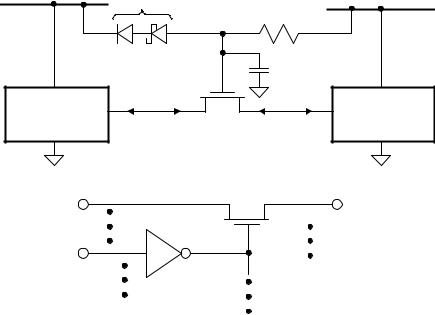
INTERNALLY CREATED VOLTAGE TOLERANCE / COMPLIANCE
The requirement for low power, high performance ICs has triggered a race among manufacturers to design devices operating at and below 2.5V that are also TTL/CMOS compatible. Figure 10.8 is a block diagram of a logic circuit that allows the logic core to operate at a reduced voltage, while the output driver operates at a standard supply voltage level of 3.3V, for example.
The technique followed by many IC manufacturers is to provide a secondary I/O ring, i.e., the I/O drivers in a 2.5V IC are driven by a 3.3V power supply, hence the device can be TTL compatible and meet the specification for VOH and VOL. The 3.3V external power supply is required for the part to be 3.3V tolerant. This causes the added complexity of two power supplies for the chip which have to be maintained in all future plug-in generations of the IC.
10.8