

ЦОС_Заочники2013 / Книги по ЦОС / Дополнительная литература / Основы ЦОС (на англ.яз) / MS3
.pdfADCS FOR DSP APPLICATIONS
SECTION 3
ADCs FOR DSP APPLICATIONS
■Successive Approximation ADCs
■Sigma-Delta ADCs
■Flash Converters
■Subranging (Pipelined) ADCs
■Bit-Per-Stage (Serial, or Ripple) ADCs
3.a
ADCS FOR DSP APPLICATIONS
3.b
ADCS FOR DSP APPLICATIONS
SECTION 3
ADCs FOR DSP APPLICATIONS
Walt Kester, James Bryant
The trend in ADCs and DACs is toward higher speeds and higher resolutions at reduced power levels and supply voltages. Modern data converters generally operate on ±5V (dual supply), +5V or +3V (single supply). In fact, the number of +3V devices is rapidly increasing because of many new markets such as digital cameras, camcorders, and cellular telephones. This trend has created a number of design and applications problems which were much less important in earlier data converters, where ±15V supplies and ±10V input ranges were the standard.
Lower supply voltages imply smaller input voltage ranges, and hence more susceptibility to noise from all potential sources: power supplies, references, digital signals, EMI/RFI, and probably most important, improper layout, grounding, and decoupling techniques. Single-supply ADCs often have an input range which is not referenced to ground. Finding compatible single-supply drive amplifiers and dealing with level shifting of the input signal in direct-coupled applications also becomes a challenge.
In spite of these issues, components are now available which allow extremely high resolutions at low supply voltages and low power. This section discusses the applications problems associated with such components and shows techniques for successfully designing them into systems.
The most popular ADCs for DSP applications are based on five fundamental architectures: successive approximation, sigma-delta, flash, subranging (or pipelined), and bit-per-stage (or ripple).
LOW POWER, LOW VOLTAGE ADC DESIGN ISSUES
■Typical Supply Voltages: ±5V, +5V, +5/+3V, +3V
■Lower Signal Swings Increase Sensitivity to
All Types of Noise (Device, Power Supply, Logic, etc.)
■Device Noise Increases at Low Currents
■Common Mode Input Voltage Restrictions
■Input Buffer Amplifier Selection Critical
■Auto-Calibration Modes Desirable at High Resolutions
Figure 3.1
3.1
ADCS FOR DSP APPLICATIONS
ADCs FOR DSP APPLICATIONS
Successive Approximation
Resolutions to 16-bits
Minimal Throughput Delay Time (No Output Latency, "Single-Shot" Operation Possible
Used in Multiplexed Data Acquisition Systems
Sigma-Delta
Resolutions to 24-bits
Excellent Differential Linearity
Internal Digital Filter (Can be Linear Phase)
Long Throughput Delay Time (Output Latency)
Difficult to Multiplex Inputs Due to Digital Filter Settling Time
High Speed Architectures:
Flash Converter
Subranging or Pipelined
Bit-Per-Stage (Ripple)
Figure 3.2
SUCCESSIVE APPROXIMATION ADCS
The successive approximation ADC has been the mainstay of signal conditioning for many years. Recent design improvements have extended the sampling frequency of these ADCs into the megahertz region. The use of internal switched capacitor techniques along with auto calibration techniques extend the resolution of these ADCs to 16-bits on standard CMOS processes without the need for expensive thinfilm laser trimming.
The basic successive approximation ADC is shown in Figure 3.3. It performs conversions on command. On the assertion of the CONVERT START command, the sample-and-hold (SHA) is placed in the hold mode, and all the bits of the successive approximation register (SAR) are reset to "0" except the MSB which is set to "1". The SAR output drives the internal DAC. If the DAC output is greater than the analog input, this bit in the SAR is reset, otherwise it is left set. The next most significant bit is then set to "1". If the DAC output is greater than the analog input, this bit in the SAR is reset, otherwise it is left set. The process is repeated with each bit in turn. When all the bits have been set, tested, and reset or not as appropriate, the contents of the SAR correspond to the value of the analog input, and the conversion is complete. These bit “tests” can form the basis of a serial output version SAR-based ADC.
3.2
ADCS FOR DSP APPLICATIONS
The end of conversion is generally indicated by an end-of-convert (EOC), data-ready (DRDY), or a busy signal (actually, not-BUSY indicates end of conversion). The polarities and name of this signal may be different for different SAR ADCs, but the fundamental concept is the same. At the beginning of the conversion interval, the signal goes high (or low) and remains in that state until the conversion is completed, at which time it goes low (or high). The trailing edge is generally an indication of valid output data.
SUCCESSIVE APPROXIMATION ADC
|
|
|
|
|
|
|
|
|
|
|
|
CONVERT |
|
|
|
|
|
|
|
|
|
|
|
|
|
START |
|
ANALOG |
|
|
|
|
|
|
|
TIMING |
|||||
|
|
|
|
|
|
|
|
|
|
||||
|
|
|
|
|
|
|
|
|
|
||||
|
|
|
|
COMPARATOR |
|
|
|
|
|
||||
|
|
|
|
|
|
|
|
|
|||||
INPUT |
SHA |
|
|
|
|
|
|
EOC, |
|||||
|
|
|
|
|
|
||||||||
|
|
|
|
|
|
|
|
|
|||||
|
|
|
|
|
|
|
|
|
|
|
|||
|
|
|
|
|
|
|
|
|
|
|
DRDY, |
||
|
|
|
|
|
|
|
|
|
|
|
|||
|
|
|
|
|
|
|
|
|
|
|
|
||
|
|
|
|
|
|
|
|
|
|
|
|
OR BUSY |
|
|
|
|
|
|
|
|
|
|
SUCCESSIVE |
|
|
|
|
|
|
|
|
|
|
|
|
|
APPROXIMATION |
|
|
|
|
|
|
|
|
|
|
|
|
|
REGISTER |
|
|
|
|
|
|
|
|
|
|
|
|
|
(SAR) |
|
|
|
|
|
|
|
|
|
|
DAC |
|
|
|
|
|
||
|
|
|
|
|
|
|
|
|
|
|
|
|
|
|
|
|
|
|
|
|
|
|
|
|
|
|
|
|
|
|
|
|
|
|
|
|
|
|
|
|
|
OUTPUT
Figure 3.3
An N-bit conversion takes N steps. It would seem on superficial examination that a 16-bit converter would have twice the conversion time of an 8-bit one, but this is not the case. In an 8-bit converter, the DAC must settle to 8-bit accuracy before the bit decision is made, whereas in a 16-bit converter, it must settle to 16-bit accuracy, which takes a lot longer. In practice, 8-bit successive approximation ADCs can convert in a few hundred nanoseconds, while 16-bit ones will generally take several microseconds.
Notice that the overall accuracy and linearity of the SAR ADC is determined primarily by the internal DAC. Until recently, most precision SAR ADCs used lasertrimmed thin-film DACs to achieve the desired accuracy and linearity. The thin-film resistor trimming process adds cost, and the thin-film resistor values may be affected when subjected to the mechanical stresses of packaging.
For these reasons, switched capacitor (or charge-redistribution) DACs have become popular in newer SAR ADCs. The advantage of the switched capacitor DAC is that the accuracy and linearity is primarily determined by photolithography, which in turn controls the capacitor plate area and the capacitance as well as matching. In
3.3
ADCS FOR DSP APPLICATIONS
addition, small capacitors can be placed in parallel with the main capacitors which can be switched in and out under control of autocalibration routines to achieve high accuracy and linearity without the need for thin-film laser trimming. Temperature tracking between the switched capacitors can be better than 1ppm/ºC, thereby offering a high degree of temperature stability.
A simple 3-bit capacitor DAC is shown in Figure 3.4. The switches are shown in the track, or sample mode where the analog input voltage, AIN, is constantly charging and discharging the parallel combination of all the capacitors. The hold mode is initiated by opening SIN, leaving the sampled analog input voltage on the capacitor array. Switch SC is then opened allowing the voltage at node A to move as the bit switches are manipulated. If S1, S2, S3, and S4 are all connected to ground, a voltage equal to –AIN appears at node A. Connecting S1 to VREF adds a voltage equal to VREF/2 to –AIN. The comparator then makes the MSB bit decision, and the SAR either leaves S1 connected to VREF or connects it to ground depending on the comparator output (which is high or low depending on whether the voltage at node A is negative or positive, respectively). A similar process is followed for the remaining two bits. At the end of the conversion interval, S1, S2, S3, S4, and SIN are connected to AIN, SC is connected to ground, and the converter is ready for another cycle.
3-BIT SWITCHED CAPACITOR DAC
|
BIT1 |
BIT2 |
BIT3 |
SC |
|
(MSB) |
|
(LSB) |
|
|
|
|
|
_ |
|
|
|
|
A |
CTOTAL = 2C |
C |
C/ 2 |
C/ 4 |
C/ 4 |
|
|
|
|
+ |
|
S1 |
S2 |
S3 |
S4 |
AIN |
|
|
|
|
SIN |
|
|
|
|
VREF |
|
|
|
|
SWITCHES SHOWN IN TRACK (SAMPLE) MODE
Figure 3.4
Note that the extra LSB capacitor (C/4 in the case of the 3-bit DAC) is required to make the total value of the capacitor array equal to 2C so that binary division is accomplished when the individual bit capacitors are manipulated.
3.4

ADCS FOR DSP APPLICATIONS
The operation of the capacitor DAC (cap DAC) is similar to an R/2R resistive DAC. When a particular bit capacitor is switched to VREF, the voltage divider created by the bit capacitor and the total array capacitance (2C) adds a voltage to node A equal to the weight of that bit. When the bit capacitor is switched to ground, the same voltage is subtracted from node A.
Because of their popularity, successive approximation ADCs are available in a wide variety of resolutions, sampling rates, input and output options, package styles, and costs. It would be impossible to attempt to list all types, but Figure 3.5 shows a number of recent Analog Devices' SAR ADCs which are representative. Note that many devices are complete data acquisition systems with input multiplexers which allow a single ADC core to process multiple analog channels.
RESOLUTION / CONVERSION TIME COMPARISON
FOR REPRESENTATIVE SINGLE-SUPPLY SAR ADCs
|
|
RESOLUTION |
SAMPLING |
POWER |
CHANNELS |
|
|
|
|
RATE |
|
|
|
|
AD7472 |
12-BITS |
1.5MSPS |
9mW |
1 |
|
|
AD7891 |
12-BITS |
500kSPS |
85mW |
8 |
|
AD7858/59 |
12-BITS |
200kSPS |
20mW |
8 |
|
|
AD7887/88 |
12-BITS |
125kSPS |
3.5mW |
8 |
|
|
AD7856/57 |
14-BITS |
285kSPS |
60mW |
8 |
|
|
|
AD7660 |
16-BITS |
100kSPS |
15mW |
1 |
|
|
AD974 |
16-BITS |
200kSPS |
120mW |
4 |
|
|
AD7664 |
16-BITS |
570kSPS |
150mW |
1 |
|
Figure 3.5
While there are some variations, the fundamental timing of most SAR ADCs is similar and relatively straightforward (see Figure 3.6). The conversion process is
initiated by asserting a CONVERT START signal. The CONVST signal is a negative-going pulse whose positive-going edge actually initiates the conversion. The internal sample-and-hold (SHA) amplifier is placed in the hold mode on this edge, and the various bits are determined using the SAR algorithm. The negative-
going edge of the CONVST pulse causes the EOC or BUSY line to go high. When the conversion is complete, the BUSY line goes low, indicating the completion of the conversion process. In most cases the trailing edge of the BUSY line can be used as an indication that the output data is valid and can be used to strobe the output data into an external register. However, because of the many variations in terminology
3.5
ADCS FOR DSP APPLICATIONS
and design, the individual data sheet should always be consulted when using a specific ADC.
TYPICAL SAR ADC TIMING
SAMPLE X |
SAMPLE X+1 |
SAMPLE X+2 |
CONVST
CONVERSION |
|
TRACK/ |
|
CONVERSION |
|
TRACK/ |
TIME |
|
ACQUIRE |
|
TIME |
|
ACQUIRE |
EOC,
BUSY
OUTPUT |
DATA |
DATA |
DATA |
X |
X+1 |
Figure 3.6
It should also be noted that some SAR ADCs require an external high frequency clock in addition to the CONVERT START command. In most cases, there is no need to synchronize the two. The frequency of the external clock, if required, generally falls in the range of 1MHz to 30MHz depending on the conversion time and resolution of the ADC. Other SAR ADCs have an internal oscillator which is used to perform the conversions and only require the CONVERT START command. Because of their architecture, SAR ADCs allow single-shot conversion at any repetition rate from DC to the converter's maximum conversion rate.
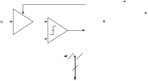
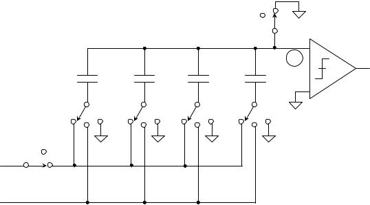
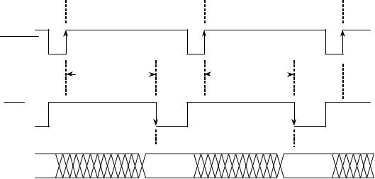
In a SAR ADC, the output data for a sampled input is valid at the end of the conversion interval for that sampled input. In other ADC architectures, such as sigma-delta or the two-stage subranging architecture shown in Figure 3.7, this is not the case. The subranging ADC shown in the figure is a two-stage pipelined or subranging 12-bit converter. The first conversion is done by the 6-bit ADC which drives a 6-bit DAC. The output of the 6-bit DAC represents a 6-bit approximation to the analog input. Note that SHA2 delays the analog signal while the 6-bit ADC makes its decision and the 6-bit DAC settles. The DAC approximation is then subtracted from the analog signal from SHA2, amplified, and digitized by a 7-bit ADC. The outputs of the two conversions are combined, and the extra bit used to correct errors made in the first conversion. The typical timing associated with this type of converter is shown in Figure 3.8. Note that the output data presented immediately after sample X actually corresponds to sample X–2, i.e., there is a two clock-cycle "pipeline" delay. The pipelined ADC architecture is generally associated with high speed ADCs, and in most cases the pipeline delay, or latency, is not a major system problem in most applications where this type of converter is used.
3.6
ADCS FOR DSP APPLICATIONS
12-BIT TWO-STAGE PIPELINED ADC ARCHITECTURE
ANALOG |
SHA |
|
SHA |
|
|
INPUT |
|
+ |
|||
|
1 |
|
|
2 |
|
|
|
|
|
|
_ |
SAMPLING |
|
|
|
|
|
CLOCK |
TIMING |
6-BIT |
|
6-BIT |
7-BIT |
|
ADC |
6 |
DAC |
ADC |
|
|
|
||||
|
|
|
|
|
|
|
|
|
BUFFER |
|
|
|
|
|
REGISTER |
|
|
|
|
|
|
6 |
7 |
|
|
|
|
|
|
|
|
|
ERROR CORRECTION LOGIC |
||
|
|
|
|
|
12 |
|
|
|
|
OUTPUT REGISTERS |
|
OUTPUT DATA |
|
12 |
|
Figure 3.7
TYPICAL PIPELINED ADC TIMING
SAMPLE X |
SAMPLE X+1 |
SAMPLE X+2 |
SAMPLING
CLOCK
OUTPUT |
DATA |
DATA |
DATA |
DATA |
X–2 |
X–1 |
X |
ABOVE SHOWS TWO CLOCK-CYCLES PIPELINE DELAY
Figure 3.8
3.7
ADCS FOR DSP APPLICATIONS
Pipelined ADCs may have more than two clock-cycles latency depending on the particular architecture. For instance, the conversion could be done in three, or four, or perhaps even more pipelined stages causing additional latency in the output data.
Therefore, if the ADC is to be used in an event-triggered (or single-shot) mode where there must be a one-to-one time correspondence between each sample and the corresponding data, then the pipeline delay can be troublesome, and the SAR architecture is advantageous. Pipeline delay or latency can also be a problem in high speed servo-loop control systems or multiplexed applications. In addition, some pipelined converters have a minimum allowable conversion rate and must be kept running to prevent saturation of internal nodes.
Switched capacitor SAR ADCs generally have unbuffered input circuits similar to the circuit shown in Figure 3.9 for the AD7858/59 ADC. During the acquisition time, the analog input must charge the 20pF equivalent input capacitance to the correct value. If the input is a DC signal, then the source resistance, RS, in series with the 125Ω internal switch resistance creates a time constant. In order to settle to 12-bit accuracy, approximately 9 time constants must be allowed for settling, and this defines the minimum allowable acquisition time. (Settling to 14-bits requires about 10 time constants, and 16-bits requires about 11).
tACQ > 9 × (RS + 125)Ω × 20pF.
For example, if RS = 50Ω, the acquisition time per the above formula must be at least 310ns.
For AC applications, a low impedance source should be used to prevent distortion due to the non-linear ADC input circuit. In a single supply application, a fast settling rail-to-rail op amp such as the AD820 should be used. Fast settling allows the op amp to settle quickly from the transient currents induced on its input by the internal ADC switches. In Figure 3.9, the AD820 drives a lowpass filter consisting of the 50Ω series resistor and the 10nF capacitor (cutoff frequency approximately 320kHz). This filter removes high frequency components which could result in aliasing and decreases the noise.
Using a single supply op amp in this application requires special consideration of signal levels. The AD820 is connected in the inverting mode and has a signal gain of –1. The noninverting input is biased at a common mode voltage of +1.3V with the 10.7kΩ/10kΩ divider, resulting in an output voltage of +2.6V for VIN= 0V, and +0.1V for VIN = +2.5V. This offset is provided because the AD820 output cannot go
all the way to ground, but is limited to the VCESAT of the output stage NPN transistor, which under these loading conditions is about 50mV. The input range of
the ADC is also offset by +100mV by applying the +100mV offset from the 412Ω/10kΩ divider to the AIN– input.
3.8