

THEORY OF OPERATION |
|
|
||||
I1 |
20µA |
VB |
20µA |
I2 |
|
|
|
A1 |
|
A2 |
|
10kΩ |
|
|
C1 |
|
C2 |
|
|
|
|
|
10kΩ |
|
|
||
|
|
|
|
|
|
|
|
|
|
|
|
A3 |
OUTPUT |
R3 |
R1 |
R2 |
10kΩ |
10kΩ |
REF |
|
|
|
|||||
400Ω |
|
|
||||
Q1 |
|
|
Q2 |
+IN |
|
|
– IN |
|
|
|
|||
|
|
RG |
|
R4 |
|
|
|
|
|
400Ω |
|
|
|
|
GAIN |
|
GAIN |
|
|
|
|
SENSE |
|
SENSE |
|
|
|
|
0-038 |
–VS |
00775- |
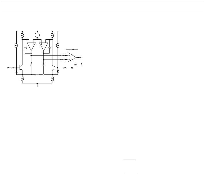
Figure 38. Simplified Schematic of AD620
The AD620 is a monolithic instrumentation amplifier based on a modification of the classic three op amp approach. Absolute value trimming allows the user to program gain accurately
(to 0.15% at G = 100) with only one resistor. Monolithic construction and laser wafer trimming allow the tight matching and tracking of circuit components, thus ensuring the high level of performance inherent in this circuit.
AD620
The input transistors Q1 and Q2 provide a single differentialpair bipolar input for high precision (Figure 38), yet offer 10× lower input bias current thanks to Superϐeta processing.
Feedback through the Q1-A1-R1 loop and the Q2-A2-R2 loop maintains constant collector current of the input devices Q1 and Q2, thereby impressing the input voltage across the external gain setting resistor RG. This creates a differential gain from the inputs to the A1/A2 outputs given by G = (R1 + R2)/RG + 1. The unity-gain subtractor, A3, removes any common-mode signal, yielding a single-ended output referred to the REF pin potential.
The value of RG also determines the transconductance of the preamp stage. As RG is reduced for larger gains, the transconductance increases asymptotically to that of the input transistors. This has three important advantages: (a) Open-loop gain is boosted for increasing programmed gain, thus reducing gain related errors. (b) The gain-bandwidth product (determined by C1 and C2 and the preamp transconductance) increases with programmed gain, thus optimizing frequency response. (c) The input voltage noise is reduced to a value of
9 nV/√Hz, determined mainly by the collector current and base resistance of the input devices.
The internal gain resistors, R1 and R2, are trimmed to an absolute value of 24.7 kΩ, allowing the gain to be programmed accurately with a single external resistor.
The gain equation is then
G = 49.4kΩ+1
RG
RG = 49.4kΩ
G−1
Make vs. Buy: a Typical Bridge Application Error Budget
The AD620 offers improved performance over “homebrew” three op amp IA designs, along with smaller size, fewer components, and 10× lower supply current. In the typical application, shown in Figure 39, a gain of 100 is required to amplify a bridge output of 20 mV full-scale over the industrial temperature range of −40°C to +85°C. Table 3 shows how to calculate the effect various error sources have on circuit accuracy.
Rev. G | Page 13 of 20
AD620
Regardless of the system in which it is being used, the AD620 provides greater accuracy at low power and price. In simple systems, absolute accuracy and drift errors are by far the most significant contributors to error. In more complex systems with an intelligent processor, an autogain/autozero cycle will remove all absolute accuracy and drift errors, leaving only the resolution errors of gain, nonlinearity, and noise, thus allowing full 14-bit accuracy.
Note that for the homebrew circuit, the OP07 specifications for input voltage offset and noise have been multiplied by √2. This is because a three op amp type in-amp has two op amps at its inputs, both contributing to the overall input error.
|
10V |
R = 350Ω |
R = 350Ω |
R = 350Ω |
R = 350Ω |
PRECISION BRIDGE TRANSDUCER |
00775-0-039 |
|
RG |
|
|
|
AD620A |
|
|
|
||||
|
499Ω |
|
|
|
|
|||||||
|
|
|
|
|
|
|
|
|
||||
|
|
|
|
|
|
|
|
|
REFERENCE |
|||
|
|
|
|
|
|
|
|
|
||||
|
|
|
|
|
|
|
|
|
||||
|
AD620A MONOLITHIC |
|
||||||||||
|
INSTRUMENTATION |
|
||||||||||
|
AMPLIFIER, G = 100 |
00775-0-040 |
||||||||||
SUPPLY CURRENT = 1.3mA MAX |
||||||||||||
|
10kΩ* |
10kΩ* |
|
OP07D |
|
|
10kΩ** |
|
100Ω** |
10kΩ** |
OP07D |
|
OP07D |
10kΩ* |
|
10kΩ* |
"HOMEBREW" IN-AMP, G = 100
*0.02% RESISTOR MATCH, 3ppm/°C TRACKING
**DISCRETE 1% RESISTOR, 100ppm/°C TRACKING
SUPPLY CURRENT = 15mA MAX
00775-0-041
Figure 39. Make vs. Buy
Table 3. Make vs. Buy Error Budget
|
|
|
Error, ppm of Full Scale |
||
Error Source |
AD620 Circuit Calculation |
“Homebrew” Circuit Calculation |
AD620 |
|
Homebrew |
|
|||||
ABSOLUTE ACCURACY at TA = 25°C |
|
|
|
|
|
Input Offset Voltage, µV |
125 µV/20 mV |
(150 µV × √2)/20 mV |
6,250 |
|
10,607 |
Output Offset Voltage, µV |
1000 µV/100 mV/20 mV |
((150 µV × 2)/100)/20 mV |
500 |
|
150 |
Input Offset Current, nA |
2 nA ×350 Ω/20 mV |
(6 nA ×350 Ω)/20 mV |
18 |
|
53 |
CMR, dB |
110 dB(3.16 ppm) ×5 V/20 mV |
(0.02% Match × 5 V)/20 mV/100 |
791 |
|
500 |
|
|
Total Absolute Error |
7,559 |
|
11,310 |
DRIFT TO 85°C |
|
|
|
|
|
Gain Drift, ppm/°C |
(50 ppm + 10 ppm) ×60°C |
100 ppm/°C Track × 60°C |
3,600 |
|
6,000 |
Input Offset Voltage Drift, µV/°C |
1 µV/°C × 60°C/20 mV |
(2.5 µV/°C × √2 × 60°C)/20 mV |
3,000 |
|
10,607 |
Output Offset Voltage Drift, µV/°C |
15 µV/°C × 60°C/100 mV/20 mV |
(2.5 µV/°C × 2 × 60°C)/100 mV/20 mV |
450 |
|
150 |
|
|
Total Drift Error |
7,050 |
|
16,757 |
|
|
|
|
|
|
RESOLUTION |
|
|
|
|
|
Gain Nonlinearity, ppm of Full Scale |
40 ppm |
40 ppm |
40 |
|
40 |
Typ 0.1 Hz to 10 Hz Voltage Noise, µV p-p |
0.28 µV p-p/20 mV |
(0.38 µV p-p × √2)/20 mV |
14 |
|
27 |
|
|
Total Resolution Error |
54 |
|
67 |
|
|
Grand Total Error |
14,663 |
|
28,134 |
|
|
|
|
|
|
G = 100, VS = ±15 V. |
|
|
|
|
|
(All errors are min/max and referred to input.) |
|
|
|
|
|
Rev. G | Page 14 of 20
AD620
|
5V |
|
|
|
|
|
|
|
|
|
7 |
20kΩ |
|
|
|
|
|
3 |
|
|
|
|
|
3kΩ |
3kΩ |
|
|
|
|
|
|
8 |
|
|
|
REF |
|
||
|
|
AD620B |
|
|
|
||
3kΩ |
3kΩ |
G = 100 |
6 |
|
IN |
DIGITAL |
|
499Ω |
5 |
10kΩ |
|
ADC |
|||
|
|
1 |
|
DATA |
|||
|
|
2 |
4 |
|
|
|
OUTPUT |
|
|
|
AD705 |
|
|
||
|
|
|
|
|
AGND |
|
|
|
|
|
|
|
20kΩ |
|
|
1.7mA |
|
|
1.3mA |
0.10mA |
0.6mA |
|
|
|
|
MAX |
|
|
|||
|
|
|
MAX |
|
|
|
|
|
|
|
|
|
|
00775-0-042 |
|
|
|
|
|
|
|
|
Figure 40. A Pressure Monitor Circuit that Operates on a 5 V Single Supply
Pressure Measurement
Although useful in many bridge applications, such as weigh scales, the AD620 is especially suitable for higher resistance pressure sensors powered at lower voltages where small size and low power become more significant.
Figure 40 shows a 3 kΩ pressure transducer bridge powered from 5 V. In such a circuit, the bridge consumes only 1.7 mA. Adding the AD620 and a buffered voltage divider allows the signal to be conditioned for only 3.8 mA of total supply current.
Small size and low cost make the AD620 especially attractive for voltage output pressure transducers. Since it delivers low noise and drift, it will also serve applications such as diagnostic noninvasive blood pressure measurement.
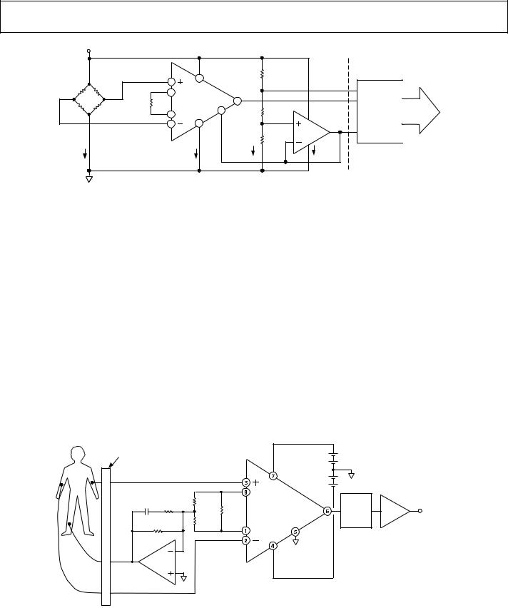
Medical ECG
The low current noise of the AD620 allows its use in ECG monitors (Figure 41) where high source resistances of 1 MΩ or higher are not uncommon. The AD620’s low power, low supply voltage requirements, and space-saving 8-lead mini-DIP and SOIC package offerings make it an excellent choice for batterypowered data recorders.
Furthermore, the low bias currents and low current noise, coupled with the low voltage noise of the AD620, improve the dynamic range for better performance.
The value of capacitor C1 is chosen to maintain stability of the right leg drive loop. Proper safeguards, such as isolation, must be added to this circuit to protect the patient from possible harm.
PATIENT/CIRCUIT |
|
|
+3V |
|
|
|
|
|
|
|
|
|
|
||
PROTECTION/ISOLATION |
|
|
|
|
|
|
|
|
R1 |
R3 |
|
|
0.03Hz |
|
|
C1 |
10kΩ |
24.9kΩ |
RG |
|
|
OUTPUT |
|
AD620A |
HIGH- |
G = 143 |
|||||
|
R4 |
R2 |
8.25kΩ |
PASS |
1V/mV |
||
|
|
G = 7 |
FILTER |
|
|
||
|
1MΩ |
24.9kΩ |
|
|
|
OUTPUT |
|
|
|
|
|
|
|
|
|
|
|
|
|
|
|
AMPLIFIER |
|
AD705J |
|
|
|
|
|
|
|
|
|
|
|
–3V |
|
|
00775-0-043 |
|
|
|
|
|
|
|
|
Figure 41. A Medical ECG Monitor Circuit
Rev. G | Page 15 of 20

AD620
Precision V-I Converter
The AD620, along with another op amp and two resistors, makes a precision current source (Figure 42). The op amp buffers the reference terminal to maintain good CMR. The output voltage, VX, of the AD620 appears across R1, which converts it to a current. This current, less only the input bias current of the op amp, then flows out to the load.
|
|
|
|
+VS |
|
VIN+ |
3 |
|
|
7 |
|
|
8 |
|
|
|
+ VX – |
RG |
|
|
|
AD620 |
|
|
|
|
6 |
||
|
1 |
|
|
5 |
R1 |
|
|
|
|
||
VIN– |
2 |
|
|
4 |
IL |
|
|
|
|
–VS |
AD705 |
|
|
|
|
|
|
I |
= |
Vx |
= |
[(VIN+) – (VIN–)] G |
|
L |
|
R1 |
|
R1 |
044-0-00775 |
|
|
|
|
|
LOAD |
Figure 42. Precision Voltage-to-Current Converter (Operates on 1.8 mA, ±3 V)
GAIN SELECTION
The AD620’s gain is resistor-programmed by RG, or more precisely, by whatever impedance appears between Pins 1 and 8. The AD620 is designed to offer accurate gains using 0.1% to 1% resistors. Table 4 shows required values of RG for various gains. Note that for G = 1, the RG pins are unconnected (RG = ∞). For any arbitrary gain, RG can be calculated by using the formula:
R = |
49.4kΩ |
G |
G −1 |
|
To minimize gain error, avoid high parasitic resistance in series with RG; to minimize gain drift, RG should have a low TC—less than 10 ppm/°C—for the best performance.
Table 4. Required Values of Gain Resistors
1% Std Table |
Calculated |
0.1% Std Table |
Calculated |
Value of RG(Ω) |
Gain |
Value of RG(Ω ) |
Gain |
|
|
|
|
49.9 k |
1.990 |
49.3 k |
2.002 |
12.4 k |
4.984 |
12.4 k |
4.984 |
5.49 k |
9.998 |
5.49 k |
9.998 |
2.61 k |
19.93 |
2.61 k |
19.93 |
1.00 k |
50.40 |
1.01 k |
49.91 |
499 |
100.0 |
499 |
100.0 |
249 |
199.4 |
249 |
199.4 |
100 |
495.0 |
98.8 |
501.0 |
49.9 |
991.0 |
49.3 |
1,003.0 |
|
|
|
|
INPUT AND OUTPUT OFFSET VOLTAGE
The low errors of the AD620 are attributed to two sources, input and output errors. The output error is divided by G when referred to the input. In practice, the input errors dominate at high gains, and the output errors dominate at low gains. The total VOS for a given gain is calculated as
Total Error RTI = input error + (output error/G)
Total Error RTO = (input error × G) + output error
REFERENCE TERMINAL
The reference terminal potential defines the zero output voltage and is especially useful when the load does not share a precise ground with the rest of the system. It provides a direct means of injecting a precise offset to the output, with an allowable range of 2 V within the supply voltages. Parasitic resistance should be kept to a minimum for optimum CMR.
INPUT PROTECTION
The AD620 features 400 Ω of series thin film resistance at its inputs and will safely withstand input overloads of up to ±15 V or ±60 mA for several hours. This is true for all gains and power on and off, which is particularly important since the signal source and amplifier may be powered separately. For longer time periods, the current should not exceed 6 mA
(IIN ≤ VIN/400 Ω). For input overloads beyond the supplies, clamping the inputs to the supplies (using a low leakage diode such as an FD333) will reduce the required resistance, yielding lower noise.
RF INTERFERENCE
All instrumentation amplifiers rectify small out of band signals. The disturbance may appear as a small dc voltage offset. High frequency signals can be filtered with a low pass R-C network placed at the input of the instrumentation amplifier. Figure 43 demonstrates such a configuration. The filter limits the input signal according to the following relationship:
FilterFreq DIFF |
= |
1 |
||||
2πR(2CD +CC ) |
||||||
FilterFreq |
CM |
= |
|
1 |
|
|
2πRCC |
||||||
|
|
|||||
where CD ≥10CC. |
|
|
|
|
||
CD affects the difference signal. CC affects the common-mode signal. Any mismatch in R × CC will degrade the AD620’s CMRR. To avoid inadvertently reducing CMRR-bandwidth performance, make sure that CC is at least one magnitude smaller than CD. The effect of mismatched CCs is reduced with a larger CD:CC ratio.
Rev. G | Page 16 of 20