

ERRORS DUE TO AC CMRR
In Table 9, the error due to common-mode rejection results from the common-mode voltage from the bridge 2.5 V. The ac error due to less than ideal common-mode rejection cannot
be calculated without knowing the size of the ac common-mode voltage (usually interference from 50 Hz/60 Hz mains frequencies).
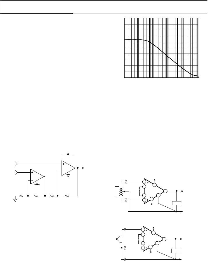
A mismatch of 0.1% between the four gain setting resistors determines the low frequency CMRR of a two op amp in-amp. The plot in Figure 42 shows the practical results of resistor mismatch at ambient temperature.
The CMRR of the circuit in Figure 43 (Gain = +11) was measured using four resistors with a mismatch of nearly 0.1% (R1 = 9999.5 Ω, R2 = 999.76 Ω, R3 = 1000.2 Ω, R4 = 9997.7 Ω). As expected, the CMRR at dc was measured at about 84 dB (calculated value is 85 dB). However, as frequency increases, CMRR quickly degrades. For example, a 200 mV p-p harmonic of the mains frequency at 180 Hz would result in an output voltage of about 800 μV. To put this in context, a 12-bit data acquisition system, with an input range of 0 V to 2.5 V, has an LSB weighting of 610 μV.
By contrast, the AD627 uses precision laser trimming of internal resistors, along with patented CMR trimming, to yield a higher dc CMRR and a wider bandwidth over which the CMRR is flat (see Figure 23).
|
|
|
+5V |
|
VIN– |
|
|
A2 |
|
|
|
1/2 |
|
|
|
|
|
VOUT |
|
VIN+ |
A1 |
|
OP296 |
|
|
|
|
||
1/2 |
|
|
|
|
|
|
|
|
|
|
OP296 |
|
|
|
|
–5V |
|
|
|
R1 |
R2 |
R3 |
R1 |
|
9999.5Ω |
999.76Ω |
1000.2Ω |
9997.7Ω |
00782-040 |
|
|
|
|
Figure 42. 0.1% Resistor Mismatch Example
AD627
|
120 |
|
|
110 |
|
|
100 |
|
(dB) |
90 |
|
80 |
||
CMRR |
||
70 |
||
|
60 |
|
|
|
|
|
|
50 |
|
|
|
|
|
|
40 |
|
|
|
|
|
|
30 |
|
|
|
|
041 |
|
|
|
|
|
00782- |
||
20 |
|
|
|
|
||
10 |
100 |
1k |
10k |
100k |
||
1 |
FREQUENCY (Hz)
Figure 43. CMRR over Frequency of Discrete In-Amp in Figure 42
GROUND RETURNS FOR INPUT BIAS CURRENTS
Input bias currents are dc currents that must flow to bias the input transistors of an amplifier. They are usually transistor base currents. When amplifying floating input sources, such as transformers,
or ac-coupled sources, there must be a direct dc path into each input so that the bias current can flow. Figure 44, Figure 45, and Figure 46 show how to provide a bias current path for the cases of, respectively, transformer coupling, a thermocouple application, and capacitive ac-coupling.
In dc-coupled resistive bridge applications, providing this path is generally not necessary because the bias current simply flows from the bridge supply through the bridge and into the amplifier.
However, if the impedance that the two inputs see are large, and differ by a large amount (>10 kΩ), the offset current of the input stage causes dc errors compatible with the input offset voltage of the amplifier.
–INPUT |
|
+V |
|
|
|
2 |
|
|
|
|
|
|
|
|
|
|
|
|
1 |
7 |
|
|
|
|
|
|
|
|
|
RG |
|
AD627 |
6 |
VOUT |
|
+INPUT |
8 |
5 |
REFERENCE |
|
|
3 |
4 |
|
|
||
|
|
LOAD |
|
|
|
|
|
–VS |
|
|
|
|
|
|
TO POWER |
-042 |
|
|
|
|
|
SUPPLY |
00782 |
|
|
|
|
GROUND |
Figure 44. Ground Returns for Bias Currents with Transformer Coupled Inputs
–INPUT |
|
+V |
|
|
|
2 |
|
|
|
|
|
|
|
|
|
|
|
|
1 |
7 |
|
|
|
|
|
|
|
|
|
RG |
|
AD627 |
6 |
VOUT |
|
+INPUT |
8 |
5 |
REFERENCE |
|
|
3 |
4 |
|
|
||
|
|
LOAD |
|
|
|
|
|
–VS |
|
|
|
|
|
|
TO POWER |
-043 |
|
|
|
|
|
SUPPLY |
00782 |
|
|
|
|
GROUND |
Figure 45. Ground Returns for Bias Currents with Thermocouple Inputs
Rev. C | Page 19 of 24
AD627 |
|
|
|
|
|
|
|
|
–INPUT 2 |
+V |
|
|
|
voltage difference between digital and analog grounds on a |
|
|
7 |
|
|
|
converter as small as possible (typically, <0.3 V). The increased |
||
|
1 |
|
|
|
noise, caused by the digital return currents of the converter |
||
|
AD627 |
|
|
|
|||
|
RG |
6 |
VOUT |
|
flowing through the analog ground plane, is generally |
||
|
8 |
5 |
REFERENCE |
|
|
negligible. To maximize isolation between analog and digital, |
|
|
+INPUT |
4 |
|
|
connect the ground planes back at the supplies. |
||
|
3 |
|
LOAD |
|
|
||
100kΩ |
100kΩ |
|
|
|
|
||
–VS |
|
TO POWER |
-044 |
If there is only one power supply available, it must be shared by |
|||
|
|
|
|||||
|
|
|
|
SUPPLY |
00782 |
both digital and analog circuitry. Figure 48 shows how to |
|
|
|
|
|
GROUND |
|||
Figure 46. Ground Returns for Bias Currents with AC-Coupled Inputs |
|
minimize interference between the digital and analog circuitry. |
|||||
LAYOUT AND GROUNDING |
|
|
As in the previous case, use separate analog and digital ground |
||||
|
|
planes or use reasonably thick traces as an alternative to a |
|||||
The use of ground planes is recommended to minimize the |
|
digital ground plane. Connect the ground planes at the ground |
|||||
|
pin of the power supply. Run separate traces (or power planes) |
||||||
impedance of ground returns (and hence, the size of dc errors). |
|||||||
from the power supply to the supply pins of the digital and |
|||||||
To isolate low level analog signals from a noisy digital |
|
||||||
|
analog circuits. Ideally, each device should have its own power |
||||||
environment, many data acquisition components have separate |
|||||||
supply trace, but they can be shared by multiple devices if a |
|||||||
analog and digital ground returns (Figure 47). Return all |
|
||||||
|
single trace is not used to route current to both digital and |
||||||
ground pins from mixed signal components, such as analog-to- |
|||||||
analog circuitry. |
|||||||
digital converters, through the high quality analog ground |
|
||||||
|
|
||||||
plane. Digital ground lines of mixed signal components should |
|
||||||
also be returned through the analog ground plane. This might |
|
||||||
seem to break the rule of separating analog and digital grounds; |
|
||||||
however, in general, there is also a requirement to keep the |
|
|
|||||
ANALOG POWER SUPPLY |
|||
|
+5V |
–5V |
GND |
0.1μF |
0.1μF |
|
0.1μF |
DIGITAL POWER SUPPLY |
|
GND |
+5V |
0.1μF
7
2 |
4 |
|
|
AD627 |
6 |
3 |
5 |
|
1 |
6 |
14 |
|
|
4 |
VIN1 |
VDD |
AGND |
DGND |
12 |
3 VIN2 ADC AD7892-2
AGND VDD
μPROCESSOR
00782-045
Figure 47. Optimal Grounding Practice for a Bipolar Supply Environment with Separate Analog and Digital Supplies
POWER SUPPLY 5V GND
0.1μF
7
2 4
AD627
3 |
5 |
0.1μF
0.1μF
|
|
1 |
|
|
|
|
|
|
|
VDD |
AGND |
DGND |
12 |
VDD |
DGND |
6 |
4 |
VIN |
AD7892-2 |
|
|
|
|
|
|
ADC |
|
μPROCESSOR |
|||
00782-046
Figure 48. Optimal Ground Practice in a Single-Supply Environment
Rev. C | Page 20 of 24
INPUT PROTECTION
As shown in the simplified schematic (Figure 35), both the inverting and noninverting inputs are clamped to the positive and negative supplies by ESD diodes. In addition, a 2 kΩ series resistor on each input provides current limiting in the event of an overvoltage. These ESD diodes can tolerate a maximum continuous current of 10 mA. So an overvoltage (that is, the amount by which the input voltage exceeds the supply voltage) of ±20 V can be tolerated. This is true for all gains, and for power on and off. This last case is particularly important because the signal source and amplifier can be powered separately.
If the overvoltage is expected to exceed 20 V, use additional external series current-limiting resistors to keep the diode current below 10 mA.
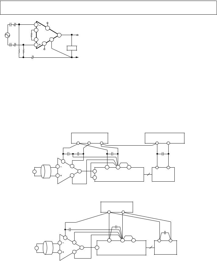
RF INTERFERENCE
All instrumentation amplifiers can rectify high frequency out- of-band signals. Once rectified, these signals appear as dc offset errors at the output. The circuit in Figure 49 provides good RFI suppression without reducing performance within the pass band of the in-amp. Resistor R1 and Capacitor C1 (and likewise, R2 and C2) form a low-pass RC filter that has a –3 dB BW equal to
F = 1/(2π(R1 × C1)).
Using the component values shown in Figure 49, this filter has a –3 dB bandwidth of approximately 8 kHz. Resistor R1 and Resistor R2 were selected to be large enough to isolate the circuit input from the capacitors, but not large enough to significantly increase circuit noise. To preserve common-mode rejection in the amplifier pass band, Capacitor C1 and Capacitor C2 must be 5% mica units, or low cost 20% units can be tested and binned to provide closely matched devices.
AD627
Capacitor C3 is needed to maintain common-mode rejection at low frequencies. R1/R2 and C1/C2 form a bridge circuit whose output appears across the input pins of the in-amp. Any mismatch between C1 and C2 unbalances the bridge and reduces common-mode rejection. C3 ensures that any RF signals are common mode (the same on both in-amp inputs) and are not applied differentially. This second low-pass network, R1 + R2 and C3, has a −3 dB frequency equal to
1/(2π((R1 + R2) × C3))
|
|
|
+VS |
|
|
|
C1 |
0.33μF |
0.01μF |
|
|
R1 |
|
|
|
|
|
1000pF |
|
|
|
|
|
20kΩ |
5% |
|
|
|
|
1% |
|
|
|
|
|
+IN |
|
|
|
|
|
R2Ω |
C3 |
RG |
AD627 |
VOUT |
|
20k |
μ |
|
|
|
|
1% |
0.022 F |
|
|
|
|
–IN |
C2 |
|
|
REFERENCE |
|
|
|
|
|
||
|
|
|
|
|
|
|
1000pF |
|
|
|
|
|
5% |
0.33μF |
0.01μF |
|
|
|
|
|
–VS |
00782-047 |
|
Figure 49. Circuit to Attenuate RF Interference
Using a C3 value of 0.022 μF, as shown in Figure 49, the −3 dB signal bandwidth of this circuit is approximately 200 Hz. The typical dc offset shift over frequency is less than 1 mV and the RF signal rejection of the circuit is better than 57 dB. To increase the 3 dB signal bandwidth of this circuit, reduce the value of Resistor R1 and Resistor R2. The performance is similar to that when using 20 kΩ resistors, except that the circuitry preceding the in-amp must drive a lower impedance load.
When building a circuit like that shown in Figure 49, use a PC board with a ground plane on both sides. Make all component leads as short as possible. Resistor R1 and Resistor R2 can be common 1% metal film units, but Capacitor C1 and Capacitor C2 must be ±5% tolerance devices to avoid degrading the commonmode rejection of the circuit. Either the traditional 5% silver mica units or Panasonic ±2% PPS film capacitors are recommended.
Rev. C | Page 21 of 24