

AD627
THEORY OF OPERATION
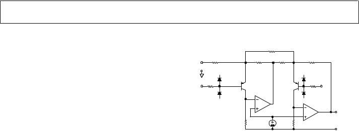
The AD627 is a true instrumentation amplifier, built using two feedback loops. Its general properties are similar to those of the classic two-op amp instrumentation amplifier configuration, but internally the details are somewhat different. The AD627 uses a modified current feedback scheme, which, coupled with interstage feedforward frequency compensation, results in a much better CMRR (common-mode rejection ratio) at frequencies above dc (notably the line frequency of 50 Hz to 60 Hz) than might otherwise be expected of a low power instrumentation amplifier.
In Figure 35, A1 completes a feedback loop, that in conjunction with V1 and R5, forces a constant collector current in Q1. Assume that the gain-setting resistor (RG) is not present. Resistor R2 and Resistor R1 complete the loop and force the output of A1 to be equal to the voltage on the inverting terminal with a gain of nearly 1.25. A2 completes a nearly identical feedback loop that forces a current in Q2 that is nearly identical to that in Q1; A2 also provides the output voltage. When both loops are balanced, the gain from the noninverting terminal to VOUT is equal to 5, whereas the gain from the output of A1 to VOUT is equal to −4. The inverting terminal gain of A1 (1.25) times the gain of A2 (−4) makes the gain from the inverting and noninverting terminals equal.
|
R1 |
REF |
100kΩ |
|
|
|
+VS |
–IN |
2kΩ |
|
|
|
–VS |
EXTERNAL GAIN RESISTOR
|
RG |
|
R4 |
|
|
|
|
100kΩ |
|
R2 |
|
R3 |
|
|
25kΩ |
25kΩ |
+VS |
|
|
|
|
|
|
|
Q1 |
|
Q2 |
2kΩ |
+IN |
A1 |
|
–VS |
|
|
|
|
|
||
|
|
|
A2 |
OUTPUT |
R5 |
V1 |
0.1V |
R6 |
033 |
200kΩ |
200kΩ |
00782- |
||
|
|
|
|
|
Figure 35. Simplified
The differential mode gain is equal to 1 + R4/R3, nominally 5, and is factory trimmed to 0.01% final accuracy. Adding an external gain setting resistor (RG) increases the gain by an amount equal to (R4 + R1)/RG. The output voltage of the AD627 is given by
VOUT = [VIN(+) – VIN(−)] × (5 + 200 kΩ/RG) + VREF
Laser trims are performed on R1 through R4 to ensure that their values are as close as possible to the absolute values in the gain equation. This ensures low gain error and high commonmode rejection at all practical gains.
Rev. C | Page 14 of 24