
- •Features
- •Disclaimer
- •Overview
- •Block Diagram
- •Pin Descriptions
- •Port B (PB7..PB0)
- •Port C (PC7..PC0)
- •Port D (PD7..PD0)
- •D-/SDATA
- •UGND
- •UVCC
- •UCAP
- •RESET/PC1/dW
- •XTAL1
- •XTAL2/PC0
- •AVR CPU Core
- •Introduction
- •Status Register
- •Stack Pointer
- •TABLE 1.
- •TABLE 2.
- •AVR AT90USB82/162 Memories
- •I/O Memory
- •Clock Systems and their Distribution
- •Clock Switch
- •Exemple of use
- •Swith from external clock to RC clock
- •Switch from RC clock to external clock
- •Clock Sources
- •Default Clock Source
- •External Clock
- •Internal PLL for USB interface
- •Idle Mode
- •Power-down Mode
- •Power-save Mode
- •Standby Mode
- •Analog Comparator
- •Brown-out Detector
- •Watchdog Timer
- •Port Pins
- •Resetting the AVR
- •Reset Sources
- •Power-on Reset
- •External Reset
- •Watchdog Reset
- •USB Reset
- •Watchdog Timer
- •TABLE 2.
- •TABLE 2.
- •Interrupts
- •TABLE 2.
- •Introduction
- •Configuring the Pin
- •Toggling the Pin
- •Reading the Pin Value
- •TABLE 3.
- •Unconnected Pins
- •Alternate Port Functions
- •Register Description for I/O-Ports
- •Timer/Counter0 and Timer/Counter1 Prescalers
- •Internal Clock Source
- •Prescaler Reset
- •External Clock Source
- •8-bit Timer/Counter0 with PWM
- •Overview
- •Registers
- •Definitions
- •Counter Unit
- •Normal Mode
- •Fast PWM Mode
- •8-bit Timer/Counter Register Description
- •Overview
- •Registers
- •Definitions
- •Counter Unit
- •Input Capture Unit
- •Noise Canceler
- •Force Output Compare
- •Normal Mode
- •Fast PWM Mode
- •16-bit Timer/Counter Register Description
- •TABLE 2.
- •TABLE 2.
- •Slave Mode
- •Master Mode
- •Data Modes
- •USART
- •Overview
- •Clock Generation
- •External Clock
- •Frame Formats
- •Parity Bit Calculation
- •TABLE 2.
- •TABLE 3.
- •TABLE 4.
- •Parity Generator
- •TABLE 3.
- •TABLE 2.
- •Receiver Error Flags
- •Parity Checker
- •Disabling the Receiver
- •TABLE 2.
- •Using MPCMn
- •Receiver Flow Control
- •Overview
- •Clock Generation
- •Frame Formats
- •TABLE 2.
- •Data Transfer
- •TABLE 3.
- •USB controller
- •Features
- •Block Diagram
- •Typical Application Implementation
- •Device mode
- •Bus Powered device
- •Introduction
- •Interrupts
- •Power modes
- •Idle mode
- •Power down
- •Freeze clock
- •Memory access capability
- •Memory management
- •PAD suspend
- •D+/D- Read/write
- •Registers description
- •USB general registers
- •USB Software Operating modes
- •USB Device Operating modes
- •Introduction
- •Power-on and reset
- •Endpoint reset
- •USB reset
- •Endpoint selection
- •Endpoint activation
- •Address Setup
- •Detach
- •Remote Wake-up
- •STALL request
- •Special consideration for Control Endpoints
- •STALL handshake and Retry mechanism
- •CONTROL endpoint management
- •Control Write
- •Control Read
- •Overview
- •“Manual” mode
- •Detailed description
- •IN endpoint management
- •“Manual” mode
- •Detailed description
- •Abort
- •Isochronous mode
- •Underflow
- •CRC Error
- •Overflow
- •Interrupts
- •Registers
- •USB device general registers
- •USB device endpoint registers
- •Characteristics
- •Analog Comparator
- •Application Section
- •Boot Reset Fuse
- •Simple Assembly Code Example for a Boot Loader
- •debugWIRE On-chip Debug System
- •Features
- •Overview
- •Physical Interface
- •Software Break Points
- •Limitations of debugWIRE
- •debugWIRE Related Register in I/O Memory
- •Fuse Bits
- •Latching of Fuses
- •Signature Bytes
- •Calibration Byte
- •Signal Names
- •Chip Erase
- •Reading the Flash
- •Reading the EEPROM
- •Electrical Characteristics
- •Absolute Maximum Ratings*
- •DC Characteristics
- •External Clock Drive Waveforms
- •External Clock Drive
- •Maximum speed vs. VCC
- •Supply Current of IO modules
- •Example 1
- •Example 2
- •Example 3
- •Instruction Set Summary
- •Packaging Information
- •TQFP32

Latching of Fuses The fuse values are latched when the device enters programming mode and changes of the fuse values will have no effect until the part leaves Programming mode. This does not apply to the EESAVE Fuse which will take effect once it is programmed. The fuses are also latched on Power-up in Normal mode.
Signature Bytes
Calibration Byte
All Atmel microcontrollers have a three-byte signature code which identifies the device. This code can be read in both serial and parallel mode, also when the device is locked. The three bytes reside in a separate address space.
AT90USB82/162 Signature Bytes:
1.0x000: 0x1E (indicates manufactured by Atmel).
2.0x001: 0x94 (indicates 16KB Flash memory).
3.0x002: 0x82 (indicates AT90USB82/162 device).
The AT90USB82/162 has a byte calibration value for the internal RC Oscillator. This byte resides in the high byte of address 0x000 in the signature address space. During reset, this byte is automatically written into the OSCCAL Register to ensure correct frequency of the calibrated RC Oscillator.
Parallel
Programming
Parameters, Pin
Mapping, and
Commands
Signal Names
This section describes how to parallel program and verify Flash Program memory, EEPROM Data memory, Memory Lock bits, and Fuse bits in the AT90USB82/162. Pulses are assumed to be at least 250 ns unless otherwise noted.
In this section, some pins of the AT90USB82/162 are referenced by signal names describing their functionality during parallel programming, see Figure 95 and Table 37. Pins not described in the following table are referenced by pin names.
The XA1/XA0 pins determine the action executed when the XTAL1 pin is given a positive pulse. The bit coding is shown in Table 40.
When pulsing WR or OE, the command loaded determines the action executed. The different commands are shown in Table 41.
236
7707A–AVR–01/07

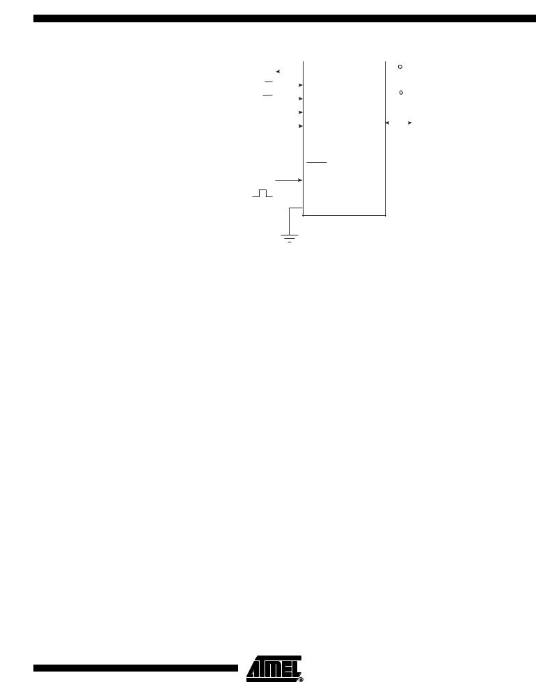
Figure 95. Parallel Programming(1)
|
|
|
|
|
|
|
|
|
|
|
+5V |
||
|
|
|
|
|
|
|
|
|
|
||||
|
|
|
|
|
|
|
|
|
|
|
|
|
|
RDY/BSY |
|
|
|
|
PD1 |
VCC |
|
|
|
|
|
||
|
OE |
|
|
|
|
PD2 |
|
|
+5V |
||||
|
|
|
|
|
|
|
|||||||
|
|
|
|
|
|||||||||
|
|
|
|
|
|
|
|
|
|
|
|||
|
WR |
|
|
|
PD3 |
AVCC |
|
|
|
|
|||
|
|
|
|
|
|
|
|
|
|||||
|
|
|
|
|
|
||||||||
|
BS1 |
|
|
|
|
PD4 |
|
|
|
DATA |
|||
|
|
|
|
PB7:0 |
|
|
|
||||||
|
|
|
|
|
|||||||||
|
XA0 |
|
|
|
|
PD5 |
|
|
|
||||
|
|
|
|
|
|
|
|
||||||
|
|
|
|
|
|
|
|
|
|
XA1 PD6
PAGEL PD7
+12 V RESET
BS2 PC6
XTAL1
GND
Note: 1. Unused Pins should be left floating.
Table 37. Pin Name Mapping
Signal Name in |
|
|
|
|
|
||||||
Programming Mode |
Pin Name |
I/O |
Function |
||||||||
|
|
|
|
|
|
|
|
|
|||
|
|
|
|
|
|
|
|
0: Device is busy programming, 1: Device is |
|||
RDY/BSY |
PD1 |
O |
|||||||||
ready for new command. |
|||||||||||
|
|
|
|
|
|
|
|
||||
|
|
|
|
|
|
|
|
||||
|
|
|
|
|
|
PD2 |
I |
Output Enable (Active low). |
|||
|
OE |
|
|
||||||||
|
|
|
|
|
|
|
|||||
|
|
|
|
|
|
PD3 |
I |
Write Pulse (Active low). |
|||
|
WR |
|
|||||||||
|
|
|
|
||||||||
BS1 |
PD4 |
I |
Byte Select 1. |
||||||||
|
|
|
|
||||||||
XA0 |
PD5 |
I |
XTAL Action Bit 0 |
||||||||
|
|
|
|
||||||||
XA1 |
PD6 |
I |
XTAL Action Bit 1 |
||||||||
|
|
|
|
||||||||
PAGEL |
PD7 |
I |
Program Memory and EEPROM data Page Load. |
||||||||
|
|
|
|
||||||||
BS2 |
PC6 |
I |
Byte Select 2. |
||||||||
|
|
|
|
||||||||
DATA |
PB7-0 |
I/O |
Bi-directional Data bus (Output when |
|
|
||||||
OE is low). |
|
||||||||||
|
|
|
|
|
|
|
|
|
|
|
Table 38. BS2 and BS1 Encoding
|
|
Flash / |
Flash Data |
|
|
|
|
EEPROM |
Loading / |
Fuse |
Reading Fuse |
BS2 |
BS1 |
Address |
Reading |
Programming |
and Lock Bits |
|
|
|
|
|
|
0 |
0 |
Low Byte |
Low Byte |
Low Byte |
Fuse Low Byte |
|
|
|
|
|
|
0 |
1 |
High Byte |
High Byte |
High Byte |
Lockbits |
|
|
|
|
|
|
1 |
0 |
Extended High |
Reserved |
Extended Byte |
Extended Fuse |
|
|
Byte |
|
|
Byte |
|
|
|
|
|
|
1 |
1 |
Reserved |
Reserved |
Reserved |
Fuse High Byte |
|
|
|
|
|
|
237
7707A–AVR–01/07

,
Table 39. Pin Values Used to Enter Programming Mode
Pin |
Symbol |
Value |
|
|
|
PAGEL |
Prog_enable[3] |
0 |
|
|
|
XA1 |
Prog_enable[2] |
0 |
|
|
|
XA0 |
Prog_enable[1] |
0 |
|
|
|
BS1 |
Prog_enable[0] |
0 |
|
|
|
Table 40. XA1 and XA0 Encoding
XA1 |
XA0 |
Action when XTAL1 is Pulsed |
|
|
|
0 |
0 |
Load Flash or EEPROM Address (High or low address byte |
|
|
determined by BS2 and BS1). |
|
|
|
0 |
1 |
Load Data (High or Low data byte for Flash determined by BS1). |
|
|
|
1 |
0 |
Load Command |
|
|
|
1 |
1 |
No Action, Idle |
|
|
|
Table 41. Command Byte Bit Encoding
Command Byte |
Command Executed |
|
|
1000 0000 |
Chip Erase |
|
|
0100 0000 |
Write Fuse bits |
|
|
0010 0000 |
Write Lock bits |
|
|
0001 0000 |
Write Flash |
|
|
0001 0001 |
Write EEPROM |
|
|
0000 1000 |
Read Signature Bytes and Calibration byte |
|
|
0000 0100 |
Read Fuse and Lock bits |
|
|
0000 0010 |
Read Flash |
|
|
0000 0011 |
Read EEPROM |
|
|
Table 42. No. of Words in a Page and No. of Pages in the Flash
|
|
|
No. of |
|
|
Flash Size |
Page Size |
PCWORD |
Pages |
PCPAGE |
PCMSB |
|
|
|
|
|
|
4/8K words (8/16Kbytes) |
64 words |
PC[5:0] |
128 |
PC[12:6] |
12 |
|
|
|
|
|
|
238
7707A–AVR–01/07

Table 43. No. of Bytes in a Page and No. of Pages in the EEPROM
|
|
|
No. of |
|
|
EEPROM Size |
Page Size |
PCWORD |
Pages |
PCPAGE |
EEAMSB |
|
|
|
|
|
|
512 bytes |
8 bytes |
EEA[2:0] |
64 |
EEA[8:3] |
8 |
|
|
|
|
|
|
239
7707A–AVR–01/07