
- •Features
- •Disclaimer
- •Overview
- •Block Diagram
- •Pin Descriptions
- •Port B (PB7..PB0)
- •Port C (PC7..PC0)
- •Port D (PD7..PD0)
- •D-/SDATA
- •UGND
- •UVCC
- •UCAP
- •RESET/PC1/dW
- •XTAL1
- •XTAL2/PC0
- •AVR CPU Core
- •Introduction
- •Status Register
- •Stack Pointer
- •TABLE 1.
- •TABLE 2.
- •AVR AT90USB82/162 Memories
- •I/O Memory
- •Clock Systems and their Distribution
- •Clock Switch
- •Exemple of use
- •Swith from external clock to RC clock
- •Switch from RC clock to external clock
- •Clock Sources
- •Default Clock Source
- •External Clock
- •Internal PLL for USB interface
- •Idle Mode
- •Power-down Mode
- •Power-save Mode
- •Standby Mode
- •Analog Comparator
- •Brown-out Detector
- •Watchdog Timer
- •Port Pins
- •Resetting the AVR
- •Reset Sources
- •Power-on Reset
- •External Reset
- •Watchdog Reset
- •USB Reset
- •Watchdog Timer
- •TABLE 2.
- •TABLE 2.
- •Interrupts
- •TABLE 2.
- •Introduction
- •Configuring the Pin
- •Toggling the Pin
- •Reading the Pin Value
- •TABLE 3.
- •Unconnected Pins
- •Alternate Port Functions
- •Register Description for I/O-Ports
- •Timer/Counter0 and Timer/Counter1 Prescalers
- •Internal Clock Source
- •Prescaler Reset
- •External Clock Source
- •8-bit Timer/Counter0 with PWM
- •Overview
- •Registers
- •Definitions
- •Counter Unit
- •Normal Mode
- •Fast PWM Mode
- •8-bit Timer/Counter Register Description
- •Overview
- •Registers
- •Definitions
- •Counter Unit
- •Input Capture Unit
- •Noise Canceler
- •Force Output Compare
- •Normal Mode
- •Fast PWM Mode
- •16-bit Timer/Counter Register Description
- •TABLE 2.
- •TABLE 2.
- •Slave Mode
- •Master Mode
- •Data Modes
- •USART
- •Overview
- •Clock Generation
- •External Clock
- •Frame Formats
- •Parity Bit Calculation
- •TABLE 2.
- •TABLE 3.
- •TABLE 4.
- •Parity Generator
- •TABLE 3.
- •TABLE 2.
- •Receiver Error Flags
- •Parity Checker
- •Disabling the Receiver
- •TABLE 2.
- •Using MPCMn
- •Receiver Flow Control
- •Overview
- •Clock Generation
- •Frame Formats
- •TABLE 2.
- •Data Transfer
- •TABLE 3.
- •USB controller
- •Features
- •Block Diagram
- •Typical Application Implementation
- •Device mode
- •Bus Powered device
- •Introduction
- •Interrupts
- •Power modes
- •Idle mode
- •Power down
- •Freeze clock
- •Memory access capability
- •Memory management
- •PAD suspend
- •D+/D- Read/write
- •Registers description
- •USB general registers
- •USB Software Operating modes
- •USB Device Operating modes
- •Introduction
- •Power-on and reset
- •Endpoint reset
- •USB reset
- •Endpoint selection
- •Endpoint activation
- •Address Setup
- •Detach
- •Remote Wake-up
- •STALL request
- •Special consideration for Control Endpoints
- •STALL handshake and Retry mechanism
- •CONTROL endpoint management
- •Control Write
- •Control Read
- •Overview
- •“Manual” mode
- •Detailed description
- •IN endpoint management
- •“Manual” mode
- •Detailed description
- •Abort
- •Isochronous mode
- •Underflow
- •CRC Error
- •Overflow
- •Interrupts
- •Registers
- •USB device general registers
- •USB device endpoint registers
- •Characteristics
- •Analog Comparator
- •Application Section
- •Boot Reset Fuse
- •Simple Assembly Code Example for a Boot Loader
- •debugWIRE On-chip Debug System
- •Features
- •Overview
- •Physical Interface
- •Software Break Points
- •Limitations of debugWIRE
- •debugWIRE Related Register in I/O Memory
- •Fuse Bits
- •Latching of Fuses
- •Signature Bytes
- •Calibration Byte
- •Signal Names
- •Chip Erase
- •Reading the Flash
- •Reading the EEPROM
- •Electrical Characteristics
- •Absolute Maximum Ratings*
- •DC Characteristics
- •External Clock Drive Waveforms
- •External Clock Drive
- •Maximum speed vs. VCC
- •Supply Current of IO modules
- •Example 1
- •Example 2
- •Example 3
- •Instruction Set Summary
- •Packaging Information
- •TQFP32

PS/2
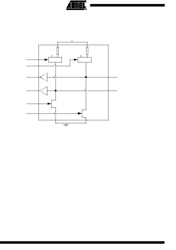
Characteristics The PS/2 pad IO’s characteristics are:
–support 5.5V (min: 4.5V, max: 5.5V)
–open drain type
–Output voltage level threshold, MCU driving low thru a 1kΩ pull-up: VOLmax = 0,7V
–fall time with 1kΩ pull-up and 500pF load: 250ns < Tfall < 1µs
–internal 2.2kΩ to 10kΩ pull-up at Vcc (5V), controlled by firmware.
–High impedance output when disabled.
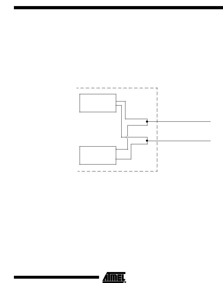
Figure 88. USB pad and PS/2 pad multiplexing
PS/2 Pad
D+ / SCK
D- / SDATA
USB Pad
Bit |
7 |
6 |
5 |
4 |
3 |
2 |
1 |
0 |
|
|
- |
- |
- |
- |
- |
- |
- |
PS2EN |
PS2CON |
|
|
|
|
|
|
|
|
|
|
Read/Write |
R |
R |
R |
R |
R |
R |
R |
R/W |
|
Initial Value |
0 |
0 |
0 |
0 |
0 |
0 |
0 |
0 |
|
• Bit 7:1 – Reserved bits
Do not set these bits.
• Bit 0 – PS2EN : PS/2 Pad Enable
Set this bit to “1” to enable the PS/2 pad.
Set this bit to “0” to disable the PS/2 pad.
For more information about pad driving, see “USB/PS2 Software Output Enable register – UPOE” on page 190.
The UPOE register described in this section allows to read or writes values on the pad. PS/2 protocol must be entirely handled by software.
213
7707A–AVR–01/07

Figure 89. PS/2 Pad description |
|
|
|
|
Vcc |
|
note: pull-up between 2.2k and 10k |
Z |
4.7kΩ |
Z |
4.7kΩ |
|
|
|
SDATA |
|
|
|
SCK |
Table 19. PS/2 DC parameters
Symbol |
Parameter |
Condition |
Min. |
Typ. |
Max. |
|
|
|
|
|
|
UVCC |
PS/2 power supply |
|
4.0V |
4.5V |
5.5V |
|
|
|
|
|
|
VIL |
Input Low Voltage |
UVCC = 4.5V - 5.5V |
|
|
0.7V |
VIH |
Input High Voltage |
UVCC = 4.5V - 5.5V |
2.4V |
|
|
RIH |
Pull-up resistor |
UVCC = 4.5V - 5.5V |
4.4kΩ |
5.1kΩ |
6.5kΩ |
Table 20. PS/2 AC parameters
Symbol |
Parameter |
Condition |
Min. |
Typ. |
Max. |
|
|
|
|
|
|
|
|
UVCC = 4.5V - 5.5V |
|
|
|
Tfall_output |
Fall time |
10% - 90% |
330ns |
375ns |
450ns |
|
|
Rload = 1kΩ, Cload = 500pF |
|
|
|
Tspike |
Spike width filtering |
|
|
|
60ns |
214
7707A–AVR–01/07