

a transmit function that handles 9-bit characters. For the assembly code, the data to be sent is
assumed to be stored in registers R17:R16.
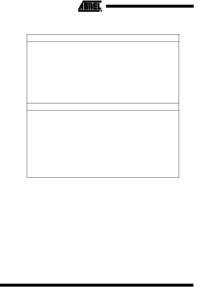
TABLE 4.
Assembly Code Example(1)(2)
USART_Transmit:
; Wait for empty transmit buffer
sbis |
UCSRnA,UDREn |
rjmp |
USART_Transmit |
; Copy 9th bit from r17 to TXB8 |
|
cbi |
UCSRnB,TXB8 |
sbrc |
r17,0 |
sbi |
UCSRnB,TXB8 |
; Put LSB data (r16) into buffer, sends the data out UDRn,r16
ret
C Code Example(1)(2)
void USART_Transmit( unsigned int data )
{
/* Wait for empty transmit buffer */ while ( !( UCSRnA & (1<<UDREn))) )
;
/* Copy 9th bit to TXB8 */ UCSRnB &= ~(1<<TXB8);
if ( data & 0x0100 ) UCSRnB |= (1<<TXB8);
/* Put data into buffer, sends the data */ UDRn = data;
}
Notes: 1. These transmit functions are written to be general functions. They can be optimized if the contents of the UCSRnB is static. For example, only the TXB8 bit of the UCSRnB Register is used after initialization.
2. See “About Code Examples” on page 6.
The ninth bit can be used for indicating an address frame when using multi processor communication mode or for other protocol handling as for example synchronization.
152
7707A–AVR–01/07
Transmitter Flags and The USART Transmitter has two flags that indicate its state: USART Data Register Empty
Interrupts |
(UDREn) and Transmit Complete (TXCn). Both flags can be used for generating interrupts. |
|
The Data Register Empty (UDREn) Flag indicates whether the transmit buffer is ready to receive |
|
new data. This bit is set when the transmit buffer is empty, and cleared when the transmit buffer |
|
contains data to be transmitted that has not yet been moved into the Shift Register. For compat- |
|
ibility with future devices, always write this bit to zero when writing the UCSRnA Register. |
|
When the Data Register Empty Interrupt Enable (UDRIEn) bit in UCSRnB is written to one, the |
|
USART Data Register Empty Interrupt will be executed as long as UDREn is set (provided that |
|
global interrupts are enabled). UDREn is cleared by writing UDRn. When interrupt-driven data |
|
transmission is used, the Data Register Empty interrupt routine must either write new data to |
|
UDRn in order to clear UDREn or disable the Data Register Empty interrupt, otherwise a new |
|
interrupt will occur once the interrupt routine terminates. |
|
The Transmit Complete (TXCn) Flag bit is set one when the entire frame in the Transmit Shift |
|
Register has been shifted out and there are no new data currently present in the transmit buffer. |
|
The TXCn Flag bit is automatically cleared when a transmit complete interrupt is executed, or it |
|
can be cleared by writing a one to its bit location. The TXCn Flag is useful in half-duplex commu- |
|
nication interfaces (like the RS-485 standard), where a transmitting application must enter |
|
receive mode and free the communication bus immediately after completing the transmission. |
|
When the Transmit Compete Interrupt Enable (TXCIEn) bit in UCSRnB is set, the USART |
|
Transmit Complete Interrupt will be executed when the TXCn Flag becomes set (provided that |
|
global interrupts are enabled). When the transmit complete interrupt is used, the interrupt han- |
|
dling routine does not have to clear the TXCn Flag, this is done automatically when the interrupt |
|
is executed. |
Parity Generator |
The Parity Generator calculates the parity bit for the serial frame data. When parity bit is enabled |
|
(UPMn1 = 1), the transmitter control logic inserts the parity bit between the last data bit and the |
|
first stop bit of the frame that is sent. |
Disabling the |
The disabling of the Transmitter (setting the TXEN to zero) will not become effective until ongo- |
Transmitter |
ing and pending transmissions are completed, i.e., when the Transmit Shift Register and |
|
Transmit Buffer Register do not contain data to be transmitted. When disabled, the Transmitter |
|
will no longer override the TxDn pin. |
Data Reception –
The USART
Receiver
The USART Receiver is enabled by writing the Receive Enable (RXENn) bit in the
UCSRnB Register to one. When the Receiver is enabled, the normal pin operation of the RxDn pin is overridden by the USART and given the function as the Receiver’s serial input. The baud rate, mode of operation and frame format must be set up once before any serial reception can be done. If synchronous operation is used, the clock on the XCKn pin will be used as transfer clock.
Receiving Frames with The Receiver starts data reception when it detects a valid start bit. Each bit that follows the start 5 to 8 Data Bits bit will be sampled at the baud rate or XCKn clock, and shifted into the Receive Shift Register until the first stop bit of a frame is received. A second stop bit will be ignored by the Receiver.
When the first stop bit is received, i.e., a complete serial frame is present in the Receive Shift Register, the contents of the Shift Register will be moved into the receive buffer. The receive buffer can then be read by reading the UDRn I/O location.
The following code example shows a simple USART receive function based on polling of the Receive Complete (RXCn) Flag. When using frames with less than eight bits the most significant
153
7707A–AVR–01/07
bits of the data read from the UDRn will be masked to zero. The USART has to be initialized
before the function can be used.
TABLE 3.
|
Assembly Code Example(1) |
|
|
|
|
|
|
|
USART_Receive: |
|
|
|
; Wait for data to be received |
|
|
|
sbis UCSRnA, RXCn |
|
|
|
rjmp USART_Receive |
|
|
|
; Get and return received data from buffer |
|
|
|
in |
r16, UDRn |
|
|
ret |
|
|
|
|
|
|
|
C Code Example(1) |
|
|
|
|
|
|
|
unsigned char USART_Receive( void ) |
|
|
|
{ |
|
|
|
/* Wait for data to be received */ |
|
|
|
while ( !(UCSRnA & (1<<RXCn)) ) |
|
|
|
|
; |
|
|
/* Get and return received data from buffer */ |
|
|
|
return UDRn; |
|
|
|
} |
|
|
|
|
|
|
|
Note: 1. |
See “About Code Examples” on page 6. |
|
|
The function simply waits for data to be present in the receive buffer by checking the RXCn Flag, |
||
|
before reading the buffer and returning the value. |
||
Receiving Frames with |
If 9-bit characters are used (UCSZn=7) the ninth bit must be read from the RXB8n bit in UCS- |
||
9 Data Bits |
RnB before reading the low bits from the UDRn. This rule applies to the FEn, DORn and UPEn |
||
|
Status Flags as well. Read status from UCSRnA, then data from UDRn. Reading the UDRn I/O |
||
|
location will change the state of the receive buffer FIFO and consequently the TXB8n, FEn, |
||
|
DORn and UPEn bits, which all are stored in the FIFO, will change. |
||
The following code example shows a simple USART receive function that handles both nine bit characters and the status bits.
154
7707A–AVR–01/07
TABLE 2.
Assembly Code Example(1)
USART_Receive:
; Wait for data to be received
sbis UCSRnA, RXCn rjmp USART_Receive
; Get status and 9th bit, then data from buffer
in |
r18, UCSRnA |
in |
r17, UCSRnB |
in |
r16, UDRn |
; If |
error, return -1 |
andi |
r18,(1<<FEn)|(1<<DORn)|(1<<UPEn) |
breq |
USART_ReceiveNoError |
ldi |
r17, HIGH(-1) |
ldi |
r16, LOW(-1) |
USART_ReceiveNoError:
; Filter the 9th bit, then return lsr r17
andi r17, 0x01
ret
C Code Example(1)
unsigned int USART_Receive( void )
{
unsigned char status, resh, resl; /* Wait for data to be received */ while ( !(UCSRnA & (1<<RXCn)) )
;
/* Get status and 9th bit, then data */ /* from buffer */
status = UCSRnA; resh = UCSRnB; resl = UDRn;
/* If error, return -1 */
if ( status & (1<<FEn)|(1<<DORn)|(1<<UPEn) ) return -1;
/* Filter the 9th bit, then return */ resh = (resh >> 1) & 0x01;
return ((resh << 8) | resl);
}
Note: 1. See “About Code Examples” on page 6.
The receive function example reads all the I/O Registers into the Register File before any computation is done. This gives an optimal receive buffer utilization since the buffer location read will be free to accept new data as early as possible.
155
7707A–AVR–01/07