


16-bit Timer/Counter Register Description
Timer/Counter1
Control Register A –
TCCR1A
|
|
|
|
|
|
|
|
|
|
|
|
|
|
|
|
|
|
|
|
|
|
|
|
|
|
Bit |
7 |
6 |
5 |
4 |
|
|
3 |
2 |
1 |
0 |
|
|
|
|
|
|
|
|
|
|
|
|
|||
|
COM1A |
COM1A |
COM1B |
COM1B |
COM1C |
COM1C |
WGM11 |
WGM1 |
TCCR1 |
|||
|
1 |
0 |
1 |
0 |
|
|
1 |
0 |
|
0 |
A |
|
|
|
|
|
|
|
|
|
|
|
|||
Read/Write |
R/W |
R/W |
R/W |
R/W |
R/W |
R/W |
R/W |
R/W |
|
|||
Initial Value |
0 |
0 |
0 |
0 |
|
|
0 |
0 |
0 |
0 |
|
|
•Bit 7:6 – COMnA1:0: Compare Output Mode for Channel A
•Bit 5:4 – COMnB1:0: Compare Output Mode for Channel B
•Bit 3:2 – COMnC1:0: Compare Output Mode for Channel C
The COMnA1:0, COMnB1:0, and COMnC1:0 control the output compare pins (OCnA, OCnB, and OCnC respectively) behavior. If one or both of the COMnA1:0 bits are written to one, the OCnA output overrides the normal port functionality of the I/O pin it is connected to. If one or both of the COMnB1:0 bits are written to one, the OCnB output overrides the normal port functionality of the I/O pin it is connected to. If one or both of the COMnC1:0 bits are written to one, the OCnC output overrides the normal port functionality of the I/O pin it is connected to. However, note that the Data Direction Register (DDR) bit corresponding to the OCnA, OCnB or OCnC pin must be set in order to enable the output driver.
When the OCnA, OCnB or OCnC is connected to the pin, the function of the COMnx1:0 bits is dependent of the WGMn3:0 bits setting. Table 50 shows the COMnx1:0 bit functionality when the WGMn3:0 bits are set to a normal or a CTC mode (non-PWM).
126
7707A–AVR–01/07

.
Table 50. Compare Output Mode, non-PWM
COMnA1/COMnB1/ |
COMnA0/COMnB0/ |
|
COMnC1 |
COMnC0 |
Description |
|
|
|
0 |
0 |
Normal port operation, OCnA/OCnB/OCnC |
|
|
disconnected. |
|
|
|
0 |
1 |
Toggle OCnA/OCnB/OCnC on compare |
|
|
match. |
|
|
|
1 |
0 |
Clear OCnA/OCnB/OCnC on compare |
|
|
match (set output to low level). |
|
|
|
1 |
1 |
Set OCnA/OCnB/OCnC on compare match |
|
|
(set output to high level). |
|
|
|
Table 51 shows the COMnx1:0 bit functionality when the WGMn3:0 bits are set to the fast PWM mode.
Table 51. Compare Output Mode, Fast PWM
COMnA1/COMnB1/ |
COMnA0/COMnB0/ |
|
COMnC0 |
COMnC0 |
Description |
|
|
|
0 |
0 |
Normal port operation, OCnA/OCnB/OCnC |
|
|
disconnected. |
|
|
|
0 |
1 |
WGM13:0 = 14 or 15: Toggle OC1A on |
|
|
Compare Match, OC1B and OC1C |
|
|
disconnected (normal port operation). For all |
|
|
other WGM1 settings, normal port operation, |
|
|
OC1A/OC1B/OC1C disconnected. |
|
|
|
1 |
0 |
Clear OCnA/OCnB/OCnC on compare |
|
|
match, set OCnA/OCnB/OCnC at TOP |
|
|
|
1 |
1 |
Set OCnA/OCnB/OCnC on compare match, |
|
|
clear OCnA/OCnB/OCnC at TOP |
|
|
|
Note: A special case occurs when OCRnA/OCRnB/OCRnC equals TOP and COMnA1/COMnB1/COMnC1 is set. In this case the compare match is ignored, but the set or clear is done at TOP. See “Fast PWM Mode” on page 93. for more details.
Table 52 shows the COMnx1:0 bit functionality when the WGMn3:0 bits are set to the phase correct and frequency correct PWM mode.
127
7707A–AVR–01/07

Table 52. Compare Output Mode, Phase Correct and Phase and Frequency Correct PWM
COMnA1/COMnB/ |
COMnA0/COMnB0/ |
|
|
|
COMnC1 |
COMnC0 |
|
Description |
|
|
|
|
|
|
0 |
0 |
|
Normal port operation, OCnA/OCnB/OCnC |
|
|
|
|
disconnected. |
|
|
|
|
|
|
0 |
1 |
|
WGM13:0 = 8, 9 10 or 11: Toggle OC1A on |
|
|
|
|
Compare Match, OC1B and OC1C |
|
|
|
|
disconnected (normal port operation). For all |
|
|
|
|
other WGM1 settings, normal port operation, |
|
|
|
|
OC1A/OC1B/OC1C disconnected. |
|
|
|
|
|
|
1 |
0 |
|
Clear OCnA/OCnB/OCnC on compare |
|
|
|
|
match when up-counting. Set |
|
|
|
|
OCnA/OCnB/OCnC on compare match |
|
|
|
|
when downcounting. |
|
|
|
|
|
|
1 |
1 |
|
Set OCnA/OCnB/OCnC on compare match |
|
|
|
|
when up-counting. Clear |
|
|
|
|
OCnA/OCnB/OCnC on compare match |
|
|
|
|
when downcounting. |
|
|
|
|
|
|
Note: A special |
case occurs when |
OCRnA/OCRnB/OCRnC equals TOP and |
||
COMnA1/COMnB1//COMnC1 is set. See “Phase Correct PWM Mode” on page 94. for more details.
• Bit 1:0 – WGMn1:0: Waveform Generation Mode
Combined with the WGMn3:2 bits found in the TCCRnB Register, these bits control the counting sequence of the counter, the source for maximum (TOP) counter value, and what type of waveform generation to be used, see Table 53. Modes of operation supported by the Timer/Counter unit are: Normal mode (counter), Clear Timer on Compare match (CTC) mode, and three types of Pulse Width Modulation (PWM) modes. (See “Modes of Operation” on page 91.).
128
7707A–AVR–01/07

Table 53. Waveform Generation Mode Bit Description(1)
|
|
WGMn2 |
WGMn1 |
WGMn0 |
Timer/Counter Mode of |
|
Update of |
TOVn Flag |
Mode |
WGMn3 |
(CTCn) |
(PWMn1) |
(PWMn0) |
Operation |
TOP |
OCRnx at |
Set on |
|
|
|
|
|
|
|
|
|
0 |
0 |
0 |
0 |
0 |
Normal |
0xFFFF |
Immediate |
MAX |
|
|
|
|
|
|
|
|
|
1 |
0 |
0 |
0 |
1 |
PWM, Phase Correct, 8-bit |
0x00FF |
TOP |
BOTTOM |
|
|
|
|
|
|
|
|
|
2 |
0 |
0 |
1 |
0 |
PWM, Phase Correct, 9-bit |
0x01FF |
TOP |
BOTTOM |
|
|
|
|
|
|
|
|
|
3 |
0 |
0 |
1 |
1 |
PWM, Phase Correct, 10-bit |
0x03FF |
TOP |
BOTTOM |
|
|
|
|
|
|
|
|
|
4 |
0 |
1 |
0 |
0 |
CTC |
OCRnA |
Immediate |
MAX |
|
|
|
|
|
|
|
|
|
5 |
0 |
1 |
0 |
1 |
Fast PWM, 8-bit |
0x00FF |
TOP |
TOP |
|
|
|
|
|
|
|
|
|
6 |
0 |
1 |
1 |
0 |
Fast PWM, 9-bit |
0x01FF |
TOP |
TOP |
|
|
|
|
|
|
|
|
|
7 |
0 |
1 |
1 |
1 |
Fast PWM, 10-bit |
0x03FF |
TOP |
TOP |
|
|
|
|
|
|
|
|
|
8 |
1 |
0 |
0 |
0 |
PWM, Phase and Frequency |
ICRn |
BOTTOM |
BOTTOM |
|
|
|
|
|
Correct |
|
|
|
|
|
|
|
|
|
|
|
|
9 |
1 |
0 |
0 |
1 |
PWM, Phase and Frequency |
OCRnA |
BOTTOM |
BOTTOM |
|
|
|
|
|
Correct |
|
|
|
|
|
|
|
|
|
|
|
|
10 |
1 |
0 |
1 |
0 |
PWM, Phase Correct |
ICRn |
TOP |
BOTTOM |
|
|
|
|
|
|
|
|
|
11 |
1 |
0 |
1 |
1 |
PWM, Phase Correct |
OCRnA |
TOP |
BOTTOM |
|
|
|
|
|
|
|
|
|
12 |
1 |
1 |
0 |
0 |
CTC |
ICRn |
Immediate |
MAX |
|
|
|
|
|
|
|
|
|
13 |
1 |
1 |
0 |
1 |
(Reserved) |
– |
– |
– |
|
|
|
|
|
|
|
|
|
14 |
1 |
1 |
1 |
0 |
Fast PWM |
ICRn |
TOP |
TOP |
|
|
|
|
|
|
|
|
|
15 |
1 |
1 |
1 |
1 |
Fast PWM |
OCRnA |
TOP |
TOP |
|
|
|
|
|
|
|
|
|
Note: 1. The CTCn and PWMn1:0 bit definition names are obsolete. Use the WGMn2:0 definitions. However, the functionality and location of these bits are compatible with previous versions of the timer.
Timer/Counter1
Control Register B –
TCCR1B
Bit |
7 |
6 |
5 |
4 |
3 |
2 |
1 |
0 |
|
|
ICNC1 |
ICES1 |
– |
WGM13 |
WGM12 |
CS12 |
CS11 |
CS10 |
TCCR1B |
|
|
|
|
|
|
|
|
|
|
Read/Write |
R/W |
R/W |
R |
R/W |
R/W |
R/W |
R/W |
R/W |
|
Initial Value |
0 |
0 |
0 |
0 |
0 |
0 |
0 |
0 |
|
• Bit 7 – ICNCn: Input Capture Noise Canceler
Setting this bit (to one) activates the Input Capture Noise Canceler. When the Noise Canceler is activated, the input from the Input Capture Pin (ICPn) is filtered. The filter function requires four successive equal valued samples of the ICPn pin for changing its output. The input capture is therefore delayed by four Oscillator cycles when the noise canceler is enabled.
• Bit 6 – ICESn: Input Capture Edge Select
This bit selects which edge on the Input Capture Pin (ICPn) that is used to trigger a capture event. When the ICESn bit is written to zero, a falling (negative) edge is used as trigger, and when the ICESn bit is written to one, a rising (positive) edge will trigger the capture.
When a capture is triggered according to the ICESn setting, the counter value is copied into the Input Capture Register (ICRn). The event will also set the Input Capture Flag (ICFn), and this can be used to cause an Input Capture Interrupt, if this interrupt is enabled.
129
7707A–AVR–01/07

Timer/Counter1
Control Register C –
TCCR1C
130
When the ICRn is used as TOP value (see description of the WGMn3:0 bits located in the TCCRnA and the TCCRnB Register), the ICPn is disconnected and consequently the input capture function is disabled.
• Bit 5 – Reserved Bit
This bit is reserved for future use. For ensuring compatibility with future devices, this bit must be written to zero when TCCRnB is written.
• Bit 4:3 – WGMn3:2: Waveform Generation Mode
See TCCRnA Register description.
• Bit 2:0 – CSn2:0: Clock Select
The three clock select bits select the clock source to be used by the Timer/Counter, see Figure 35 and Figure 36.
Table 54. Clock Select Bit Description
CSn2 |
CSn1 |
CSn0 |
Description |
|
|
|
|
0 |
0 |
0 |
No clock source. (Timer/Counter stopped) |
|
|
|
|
0 |
0 |
1 |
clkI/O/1 (No prescaling |
|
|
|
|
0 |
1 |
0 |
clkI/O/8 (From prescaler) |
|
|
|
|
0 |
1 |
1 |
clkI/O/64 (From prescaler) |
|
|
|
|
1 |
0 |
0 |
clkI/O/256 (From prescaler) |
|
|
|
|
1 |
0 |
1 |
clkI/O/1024 (From prescaler) |
|
|
|
|
1 |
1 |
0 |
External clock source on Tn pin. Clock on falling edge |
|
|
|
|
1 |
1 |
1 |
External clock source on Tn pin. Clock on rising edge |
|
|
|
|
If external pin modes are used for the Timer/Countern, transitions on the Tn pin will clock the counter even if the pin is configured as an output. This feature allows software control of the counting.
Bit |
7 |
6 |
5 |
4 |
3 |
2 |
1 |
0 |
|
|
FOC1A |
FOC1B |
FOC1C |
– |
– |
– |
– |
– |
TCCR1C |
|
|
|
|
|
|
|
|
|
|
Read/Write |
W |
W |
W |
R |
R |
R |
R |
R |
|
Initial Value |
0 |
0 |
0 |
0 |
0 |
0 |
0 |
0 |
|
•Bit 7 – FOCnA: Force Output Compare for Channel A
•Bit 6 – FOCnB: Force Output Compare for Channel B
•Bit 5 – FOCnC: Force Output Compare for Channel C
The FOCnA/FOCnB/FOCnC bits are only active when the WGMn3:0 bits specifies a non-PWM mode. When writing a logical one to the FOCnA/FOCnB/FOCnC bit, an immediate compare match is forced on the waveform generation unit. The OCnA/OCnB/OCnC output is changed according to its COMnx1:0 bits setting. Note that the FOCnA/FOCnB/FOCnC bits are implemented as strobes. Therefore it is the value present in the COMnx1:0 bits that determine the effect of the forced compare.
A FOCnA/FOCnB/FOCnC strobe will not generate any interrupt nor will it clear the timer in Clear Timer on Compare Match (CTC) mode using OCRnA as TOP.
The FOCnA/FOCnB/FOCnB bits are always read as zero.
7707A–AVR–01/07
Timer/Counter1 –
TCNT1H and TCNT1L
7707A–AVR–01/07
• Bit 4:0 – Reserved Bits
These bits are reserved for future use. For ensuring compatibility with future devices, these bits must be written to zero when TCCRnC is written.
Bit |
7 |
6 |
5 |
4 |
3 |
2 |
1 |
0 |
|
|
TCNT1[15:8] |
|
|
|
|
|
|
TCNT1H |
|
|
|
|
|
|
|
|
|
|
|
|
TCNT1[7:0] |
|
|
|
|
|
|
TCNT1L |
|
|
|
|
|
|
|
|
|
|
|
Read/Write |
R/W |
R/W |
R/W |
R/W |
R/W |
R/W |
R/W |
R/W |
|
Initial Value |
0 |
0 |
0 |
0 |
0 |
0 |
0 |
0 |
|
The two Timer/Counter I/O locations (TCNTnH and TCNTnL, combined TCNTn) give direct access, both for read and for write operations, to the Timer/Counter unit 16-bit counter. To ensure that both the high and low bytes are read and written simultaneously when the CPU accesses these registers, the access is performed using an 8-bit temporary High Byte Register (TEMP). This temporary register is shared by all the other 16-bit registers. See “Accessing 16-bit Registers” on page 106.
Modifying the counter (TCNTn) while the counter is running introduces a risk of missing a compare match between TCNTn and one of the OCRnx Registers.
Writing to the TCNTn Register blocks (removes) the compare match on the following timer clock for all compare units.
131

Output Compare
Register 1 A –
OCR1AH and OCR1AL
Output Compare
Register 1 B –
OCR1BH and OCR1BL
Output Compare
Register 1 C –
OCR1CH and OCR1CL
|
|
|
|
|
|
|
|
|
|
|
|
|
|
|
|
|
|
|
|
|
|
|
|
|
|
Bit |
7 |
6 |
5 |
4 |
|
3 |
2 |
1 |
0 |
|
||
|
|
|
|
|
|
|
|
|
|
|
|
|
|
|
OCR1A[15:8] |
|
|
|
|
|
|
|
|
OCR1AH |
|
|
|
|
|
|
|
|
|
|
|
|
|
|
|
|
OCR1A[7:0] |
|
|
|
|
|
|
|
|
OCR1AL |
|
|
|
|
|
|
|
|
|
|
|
|
||
Read/Write |
R/W |
R/W |
R/W |
R/W |
R/W |
R/W |
R/W |
R/W |
||||
Initial Value |
0 |
0 |
0 |
0 |
|
0 |
0 |
0 |
0 |
|
||
Bit |
7 |
6 |
5 |
4 |
|
3 |
2 |
1 |
0 |
|
||
|
|
|
|
|
|
|
|
|
|
|
|
|
|
|
OCR1B[15:8] |
|
|
|
|
|
|
|
|
OCR1BH |
|
|
|
|
|
|
|
|
|
|
|
|
|
|
|
|
OCR1B[7:0] |
|
|
|
|
|
|
|
|
OCR1BL |
|
|
|
|
|
|
|
|
|
|
|
|
||
Read/Write |
R/W |
R/W |
R/W |
R/W |
R/W |
R/W |
R/W |
R/W |
||||
Initial Value |
0 |
0 |
0 |
0 |
|
0 |
0 |
0 |
0 |
|
||
Bit |
7 |
6 |
5 |
4 |
|
3 |
2 |
1 |
0 |
|
||
|
|
|
|
|
|
|
|
|
|
|
|
|
|
|
OCR1C[15:8] |
|
|
|
|
|
|
|
|
OCR1CH |
|
|
|
|
|
|
|
|
|
|
|
|
|
|
|
|
OCR1C[7:0] |
|
|
|
|
|
|
|
|
OCR1CL |
|
|
|
|
|
|
|
|
|
|
|
|
||
Read/Write |
R/W |
R/W |
R/W |
R/W |
R/W |
R/W |
R/W |
R/W |
||||
Initial Value |
0 |
0 |
0 |
0 |
|
0 |
0 |
0 |
0 |
|
||
The Output Compare Registers contain a 16-bit value that is continuously compared with the counter value (TCNTn). A match can be used to generate an Output Compare interrupt, or to generate a waveform output on the OCnx pin.
The Output Compare Registers are 16-bit in size. To ensure that both the high and low bytes are written simultaneously when the CPU writes to these registers, the access is performed using an 8-bit temporary High Byte Register (TEMP). This temporary register is shared by all the other 16-bit registers. See “Accessing 16-bit Registers” on page 106.
Input Capture Register
1 – ICR1H and ICR1L
Bit |
7 |
6 |
5 |
4 |
3 |
2 |
1 |
0 |
|
|
ICR1[15:8] |
|
|
|
|
|
|
|
ICR1H |
|
|
|
|
|
|
|
|
|
|
|
ICR1[7:0] |
|
|
|
|
|
|
|
ICR1L |
|
|
|
|
|
|
|
|
|
|
Read/Write |
R/W |
R/W |
R/W |
R/W |
R/W |
R/W |
R/W |
R/W |
|
Initial Value |
0 |
0 |
0 |
0 |
0 |
0 |
0 |
0 |
|
IThe Input Capture is updated with the counter (TCNTn) value each time an event occurs on the ICPn pin (or optionally on the Analog Comparator output for Timer/Counter1). The Input Capture can be used for defining the counter TOP value.
The Input Capture Register is 16-bit in size. To ensure that both the high and low bytes are read simultaneously when the CPU accesses these registers, the access is performed using an 8-bit temporary High Byte Register (TEMP). This temporary register is shared by all the other 16-bit registers. See “Accessing 16-bit Registers” on page 106.
Timer/Counter1
Interrupt Mask
Register – TIMSK1
Bit |
7 |
6 |
5 |
4 |
3 |
2 |
1 |
0 |
|
|
– |
– |
ICIE1 |
– |
OCIE1 |
OCIE1B |
OCIE1A |
TOIE1 |
TIMSK1 |
|
|
|
|
|
C |
|
|
|
|
Read/Write |
R |
R |
R/W |
R |
R/W |
R/W |
R/W |
R/W |
|
Initial Value |
0 |
0 |
0 |
0 |
0 |
0 |
0 |
0 |
|
• Bit 5 – ICIEn: Timer/Countern, Input Capture Interrupt Enable
When this bit is written to one, and the I-flag in the Status Register is set (interrupts globally enabled), the Timer/Countern Input Capture interrupt is enabled. The corresponding Interrupt Vector (See “Interrupts” on page 61.) is executed when the ICFn Flag, located in TIFRn, is set.
132
7707A–AVR–01/07

Timer/Counter1
Interrupt Flag Register
– TIFR1
Bit 3 – OCIEnC: Timer/Countern, Output Compare C Match Interrupt Enable
When this bit is written to one, and the I-flag in the Status Register is set (interrupts globally enabled), the Timer/Countern Output Compare C Match interrupt is enabled. The corresponding Interrupt Vector (See “Interrupts” on page 61.) is executed when the OCFnC Flag, located in TIFRn, is set.
• Bit 2 – OCIEnB: Timer/Countern, Output Compare B Match Interrupt Enable
When this bit is written to one, and the I-flag in the Status Register is set (interrupts globally enabled), the Timer/Countern Output Compare B Match interrupt is enabled. The corresponding Interrupt Vector (See “Interrupts” on page 61.) is executed when the OCFnB Flag, located in TIFRn, is set.
• Bit 1 – OCIEnA: Timer/Countern, Output Compare A Match Interrupt Enable
When this bit is written to one, and the I-flag in the Status Register is set (interrupts globally enabled), the Timer/Countern Output Compare A Match interrupt is enabled. The corresponding Interrupt Vector (See “Interrupts” on page 61.) is executed when the OCFnA Flag, located in TIFRn, is set.
• Bit 0 – TOIEn: Timer/Countern, Overflow Interrupt Enable
When this bit is written to one, and the I-flag in the Status Register is set (interrupts globally enabled), the Timer/Countern Overflow interrupt is enabled. The corresponding Interrupt Vector (See “Interrupts” on page 61.) is executed when the TOVn Flag, located in TIFRn, is set.
Bit |
7 |
6 |
5 |
4 |
3 |
2 |
1 |
0 |
|
|
– |
– |
ICF1 |
– |
OCF1C |
OCF1B |
OCF1A |
TOV1 |
TIFR1 |
Read/Write |
R |
R |
R/W |
R |
R/W |
R/W |
R/W |
R/W |
|
Initial Value |
0 |
0 |
0 |
0 |
0 |
0 |
0 |
0 |
|
• Bit 5 – ICFn: Timer/Countern, Input Capture Flag
This flag is set when a capture event occurs on the ICPn pin. When the Input Capture Register (ICRn) is set by the WGMn3:0 to be used as the TOP value, the ICFn Flag is set when the counter reaches the TOP value.
ICFn is automatically cleared when the Input Capture Interrupt Vector is executed. Alternatively, ICFn can be cleared by writing a logic one to its bit location.
• Bit 3– OCFnC: Timer/Countern, Output Compare C Match Flag
This flag is set in the timer clock cycle after the counter (TCNTn) value matches the Output Compare Register C (OCRnC).
Note that a Forced Output Compare (FOCnC) strobe will not set the OCFnC Flag.
OCFnC is automatically cleared when the Output Compare Match C Interrupt Vector is executed. Alternatively, OCFnC can be cleared by writing a logic one to its bit location.
• Bit 2 – OCFnB: Timer/Counter1, Output Compare B Match Flag
This flag is set in the timer clock cycle after the counter (TCNTn) value matches the Output Compare Register B (OCRnB).
Note that a Forced Output Compare (FOCnB) strobe will not set the OCFnB Flag.
OCFnB is automatically cleared when the Output Compare Match B Interrupt Vector is executed. Alternatively, OCFnB can be cleared by writing a logic one to its bit location.
• Bit 1 – OCF1A: Timer/Counter1, Output Compare A Match Flag
133
7707A–AVR–01/07

This flag is set in the timer clock cycle after the counter (TCNTn value matches the Output Compare Register A (OCRnA).
Note that a Forced Output Compare (FOCnA) strobe will not set the OCFnA Flag.
OCFnA is automatically cleared when the Output Compare Match A Interrupt Vector is executed. Alternatively, OCFnA can be cleared by writing a logic one to its bit location.
• Bit 0 – TOVn: Timer/Countern, Overflow Flag
The setting of this flag is dependent of the WGMn3:0 bits setting. In Normal and CTC modes, the TOVn Flag is set when the timer overflows. Refer to Table 53 on page 129 for the TOVn Flag behavior when using another WGMn3:0 bit setting.
TOVn is automatically cleared when the Timer/Countern Overflow Interrupt Vector is executed. Alternatively, TOVn can be cleared by writing a logic one to its bit location.
134
7707A–AVR–01/07
Serial
Peripheral
Interface – SPI
The Serial Peripheral Interface (SPI) allows high-speed synchronous data transfer between the AT90USB82/162 and peripheral devices or between several AVR devices. The AT90USB82/162 SPI includes the following features:
•Full-duplex, Three-wire Synchronous Data Transfer
•Master or Slave Operation
•LSB First or MSB First Data Transfer
•Seven Programmable Bit Rates
•End of Transmission Interrupt Flag
•Write Collision Flag Protection
•Wake-up from Idle Mode
•Double Speed (CK/2) Master SPI Mode
USART can also be used in Master SPI mode, see “USART in SPI Mode” on page 171.
The Power Reduction SPI bit, PRSPI, in “Power Reduction Register 0 - PRR0” on page 43 on page 50 must be written to zero to enable SPI module.
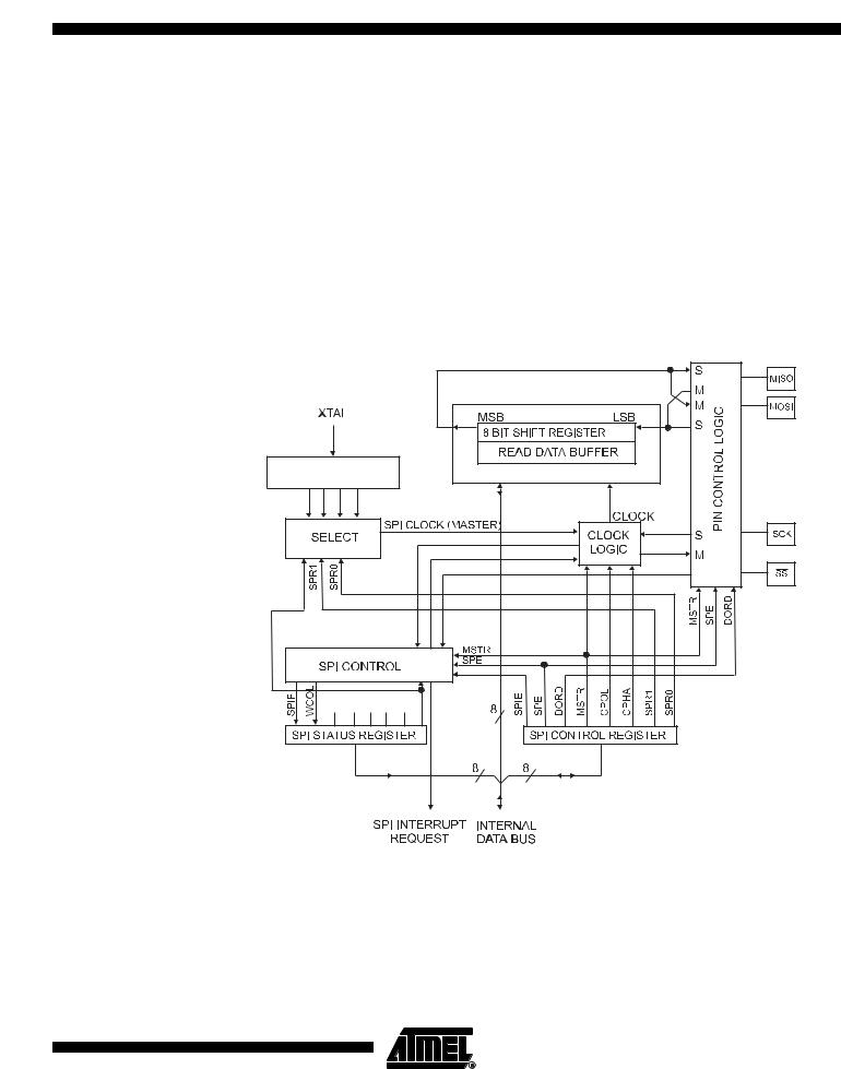
Figure 59. SPI Block Diagram(1)
DIVIDER |
/2/4/8/16/32/64/128 |
SPI2X |
SPI2X |
Note: 1. Refer to Figure 1 on page 2, and Table 31 on page 74 for SPI pin placement.
The interconnection between Master and Slave CPUs with SPI is shown in Figure 60. The system consists of two shift Registers, and a Master clock generator. The SPI Master initiates the communication cycle when pulling low the Slave Select SS pin of the desired Slave. Master and Slave prepare the data to be sent in their respective shift Registers, and the Master generates the required clock pulses on the SCK line to interchange data. Data is always shifted from Master to Slave on the Master Out – Slave In, MOSI, line, and from Slave to Master on the Master In
135
7707A–AVR–01/07
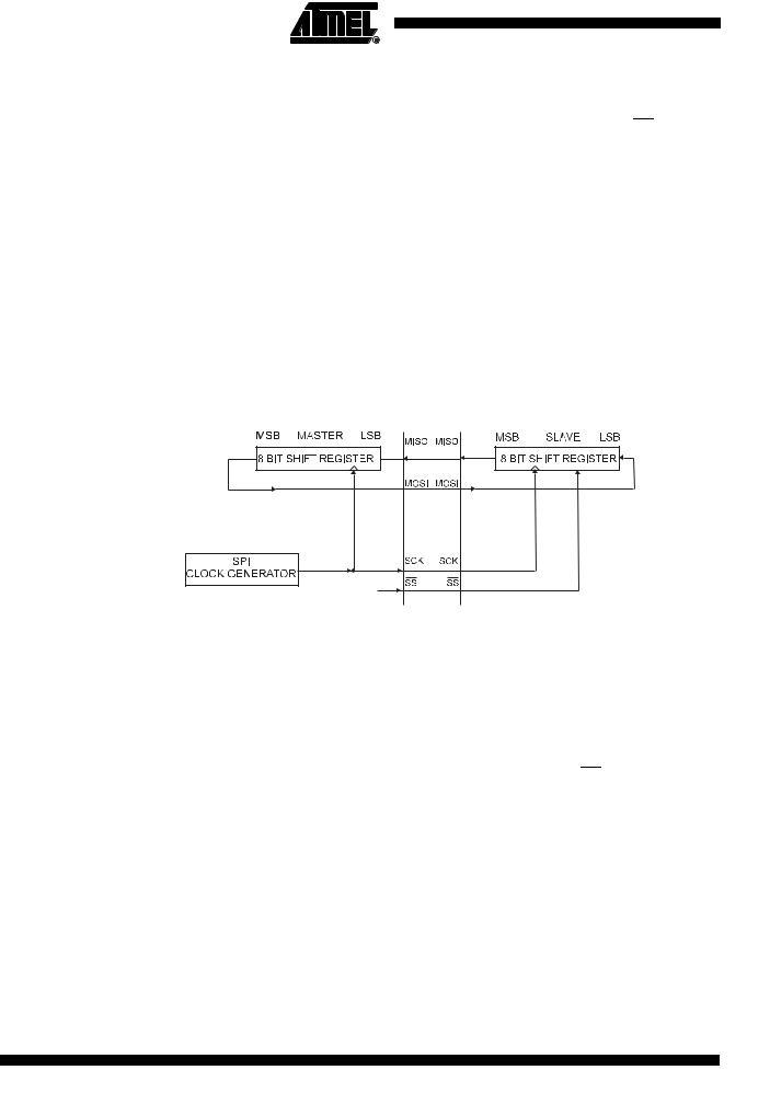
– Slave Out, MISO, line. After each data packet, the Master will synchronize the Slave by pulling high the Slave Select, SS, line.
When configured as a Master, the SPI interface has no automatic control of the SS line. This must be handled by user software before communication can start. When this is done, writing a byte to the SPI Data Register starts the SPI clock generator, and the hardware shifts the eight bits into the Slave. After shifting one byte, the SPI clock generator stops, setting the end of Transmission Flag (SPIF). If the SPI Interrupt Enable bit (SPIE) in the SPCR Register is set, an interrupt is requested. The Master may continue to shift the next byte by writing it into SPDR, or signal the end of packet by pulling high the Slave Select, SS line. The last incoming byte will be kept in the Buffer Register for later use.
When configured as a Slave, the SPI interface will remain sleeping with MISO tri-stated as long as the SS pin is driven high. In this state, software may update the contents of the SPI Data Register, SPDR, but the data will not be shifted out by incoming clock pulses on the SCK pin until the SS pin is driven low. As one byte has been completely shifted, the end of Transmission Flag, SPIF is set. If the SPI Interrupt Enable bit, SPIE, in the SPCR Register is set, an interrupt is requested. The Slave may continue to place new data to be sent into SPDR before reading the incoming data. The last incoming byte will be kept in the Buffer Register for later use.
Figure 60. SPI Master-slave Interconnection
SHIFT
ENABLE
The system is single buffered in the transmit direction and double buffered in the receive direction. This means that bytes to be transmitted cannot be written to the SPI Data Register before the entire shift cycle is completed. When receiving data, however, a received character must be read from the SPI Data Register before the next character has been completely shifted in. Otherwise, the first byte is lost.
In SPI Slave mode, the control logic will sample the incoming signal of the SCK pin. To ensure correct sampling of the clock signal, the frequency of the SPI clock should never exceed fosc/4.
When the SPI is enabled, the data direction of the MOSI, MISO, SCK, and SS pins is overridden according to Table 55. For more details on automatic port overrides, refer to “Alternate Port Functions” on page 69.
Table 55. SPI Pin Overrides(1)
Pin |
|
Direction, Master SPI |
Direction, Slave SPI |
|
|||||
|
|
|
|
|
|||||
MOSI |
|
User Defined |
Input |
|
|
||||
|
|
|
|
|
|||||
MISO |
|
Input |
User Defined |
|
|
||||
|
|
|
|
|
|||||
SCK |
|
User Defined |
Input |
|
|
||||
|
|
|
|
|
|
||||
|
|
|
|
User Defined |
Input |
|
|
||
|
SS |
|
|
|
|||||
|
|
|
|
|
|
|
|
|
|
Note: 1. |
|
|
“Alternate Functions of Port B” on page 71 |
|
|
|
|||
See |
for a detailed description of how to define the |
|
|||||||
|
|
|
direction of the user defined SPI pins. |
|
|
|
|
||
136
7707A–AVR–01/07

The following code examples show how to initialize the SPI as a Master and how to perform a simple transmission. DDR_SPI in the examples must be replaced by the actual Data Direction Register controlling the SPI pins. DD_MOSI, DD_MISO and DD_SCK must be replaced by the actual data direction bits for these pins. E.g. if MOSI is placed on pin PB5, replace DD_MOSI with DDB5 and DDR_SPI with DDRB.
137
7707A–AVR–01/07