

Watchdog Reset |
|
|
|
|
|
|
|
|
|
|
|
|
|
|
|
|
|
|
|
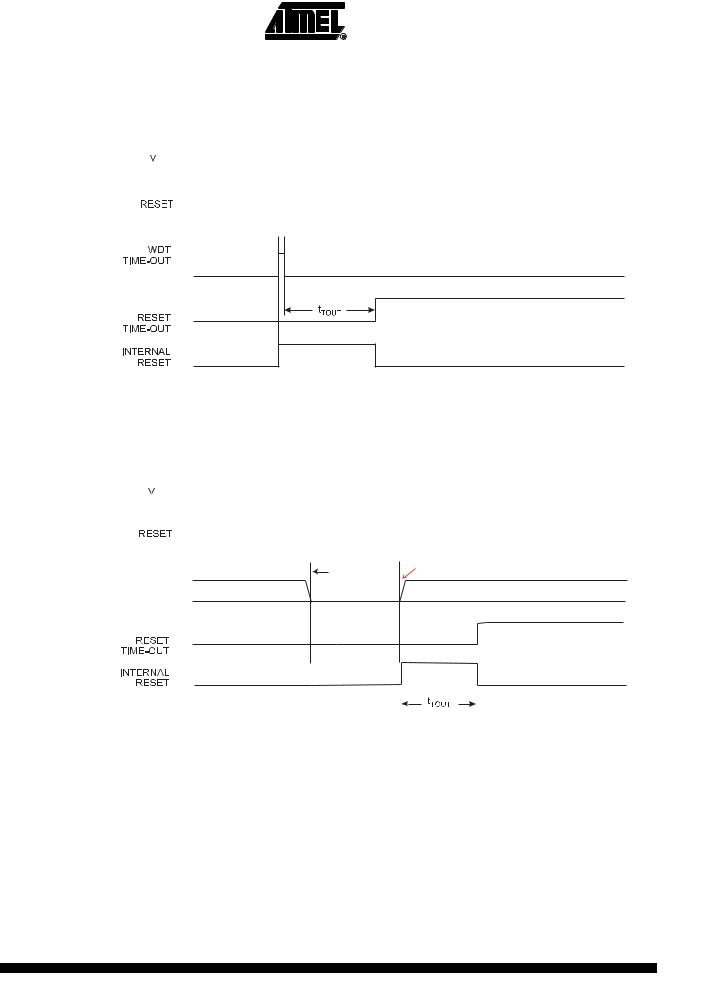
When the Watchdog times out, it will generate a short reset pulse of one CK cycle duration. On |
|||||||||
|
the falling edge of this pulse, the delay timer starts counting the Time-out period tTOUT. Refer to |
||||||||
|
on page 52 for details on operation of the Watchdog Timer. |
||||||||
|
Figure 25. Watchdog Reset During Operation |
||||||||
|
|
CC |
|
|
|||||
|
|
||||||||
|
|
|
|
|
|
|
|
|
|
|
|
|
|
|
|
|
|
|
|


 CK
CK 

USB Reset |
When the USB macro is enabled and configured with the USB reset MCU feature enabled, and |
||||
|
if a valid USB Reset signalling is detected, the microcontroller is reset unless the USB macro |
||||
|
that remains enabled. This allows the device to stay attached to the bus during and after the |
||||
|
reset, while enhancing firmware reliability. |
||||
|
Figure 26. USB Reset During Operation |
||||
|
|
CC |
|
|
|
|
|
||||
|
|
|
|
|
|
|
|
|
|
|
|
(USB Lines)
DP
DM
USB Traffic
t
USBRSTMIN 
End of Reset
USB Traffic
MCU Status Register – The MCU Status Register provides information on which reset source caused an MCU reset.
MCUSR |
Bit |
7 |
6 |
5 |
4 |
3 |
2 |
1 |
0 |
|
|
|
– |
– |
USBRF |
– |
WDRF |
BORF |
EXTRF |
PORF |
MCUSR |
|
Read/Write |
R |
R |
R |
R/W |
R/W |
R/W |
R/W |
R/W |
|
|
Initial Value |
0 |
0 |
0 |
See Bit Description |
|
|
|
|
|
• Bit 7-6 – Res: Reserved Bit
These bits are reserved and will always read as zero.
• Bit 5 – USBRF: USB Reset Flag
This bit is set if a USB Reset occurs. The bit is reset by a Power-on Reset, or by writing a logic zero to the flag.
• Bit 4– Res: Reserved Bit
50
7707A–AVR–01/07
This bit is reserved.
• Bit 3 – WDRF: Watchdog Reset Flag
This bit is set if a Watchdog Reset occurs. The bit is reset by a Power-on Reset, or by writing a logic zero to the flag.
• Bit 2 – BORF: Brown-out Reset Flag
This bit is set if a Brown-out Reset occurs. The bit is reset by a Power-on Reset, or by writing a logic zero to the flag.
• Bit 1 – EXTRF: External Reset Flag
This bit is set if an External Reset occurs. The bit is reset by a Power-on Reset, or by writing a logic zero to the flag.
• Bit 0 – PORF: Power-on Reset Flag
This bit is set if a Power-on Reset occurs. The bit is reset only by writing a logic zero to the flag.
To make use of the Reset Flags to identify a reset condition, the user should read and then Reset the MCUSR as early as possible in the program. If the register is cleared before another reset occurs, the source of the reset can be found by examining the Reset Flags.
Internal Voltage |
AT90USB82/162 features an internal bandgap reference. This reference is used for Brown-out |
||||||||
Reference |
Detection, and it can be used as an input to the Analog Comparator or the ADC. |
|
|
||||||
Voltage Reference |
The voltage reference has a start-up time that may influence the way it should be used. The |
||||||||
Enable Signals and |
start-up time is given in Table 18. To save power, the reference is not always turned on. The ref- |
||||||||
Start-up Time |
erence is on during the following situations: |
|
|
|
|
|
|
|
|
|
1. When the BOD is enabled (by programming the BODLEVEL [2..0] Fuse). |
|
|
||||||
|
2. When the bandgap reference is connected to the Analog Comparator (by setting the |
||||||||
|
ACBG bit in ACSR). |
|
|
|
|
|
|
|
|
|
3. When the ADC is enabled. |
|
|
|
|
|
|
|
|
|
Thus, when the BOD is not enabled, after setting the ACBG bit or enabling the ADC, the user |
||||||||
|
must always allow the reference to start up before the output from the Analog Comparator or |
||||||||
|
ADC is used. To reduce power consumption in Power-down mode, the user can avoid the three |
||||||||
|
conditions above to ensure that the reference is turned off before entering Power-down mode. |
||||||||
|
Table 18. Internal Voltage Reference Characteristics(1) |
|
|
|
|
|
|
||
|
Symbol |
Parameter |
Condition |
Min |
Typ |
Max |
|
Units |
|
|
|
|
|
|
|
|
|
|
|
|
VBG |
Bandgap reference voltage |
TBD |
TBD |
1.1 |
TBD |
|
V |
|
|
tBG |
Bandgap reference start-up time |
TBD |
|
40 |
70 |
|
µs |
|
|
IBG |
Bandgap reference current |
TBD |
|
10 |
TBD |
|
µA |
|
|
consumption |
|
|
|
|||||
|
Note: 1. |
Values are guidelines only. Actual values are TBD. |
|
|
|
|
|
|
|
51
7707A–AVR–01/07