


System Control
and Reset
Resetting the AVR |
During reset, all I/O Registers are set to their initial values, and the program starts execution |
||
|
from the Reset Vector. The instruction placed at the Reset Vector must be a JMP – Absolute |
||
|
Jump – instruction to the reset handling routine. If the program never enables an interrupt |
||
|
source, the Interrupt Vectors are not used, and regular program code can be placed at these |
||
|
locations. This is also the case if the Reset Vector is in the Application section while the Interrupt |
||
|
Vectors are in the Boot section or vice versa. The circuit diagram in Figure 20 shows the reset |
||
|
logic. Table 15 defines the electrical parameters of the reset circuitry. |
||
|
The I/O ports of the AVR are immediately reset to their initial state when a reset source goes |
||
|
active. This does not require any clock source to be running. |
||
|
After all reset sources have gone inactive, a delay counter is invoked, stretching the internal |
||
|
reset. This allows the power to reach a stable level before normal operation starts. The time-out |
||
|
period of the delay counter is defined by the user through the SUT and CKSEL Fuses. The dif- |
||
|
ferent selections for the delay period are presented in “Clock Sources” on page 29. |
||
Reset Sources |
The AT90USB82/162 has five sources of reset: |
||
|
• Power-on Reset. The MCU is reset when the supply voltage is below the Power-on Reset |
||
|
threshold (VPOT). |
||
|
• External Reset. The MCU is reset when a low level is present on the |
RESET |
pin for longer |
|
than the minimum pulse length. |
||
|
• Watchdog Reset. The MCU is reset when the Watchdog Timer period expires and the |
||
|
Watchdog is enabled. See “Watchdog Timer” on page 52. |
||
|
• Brown-out Reset. The MCU is reset when the supply voltage VCC is below the Brown-out |
||
|
Reset threshold (VBOT) and the Brown-out Detector is enabled. |
||
|
• USB Reset. The MCU is reset when the USB macro is enabled and detects a USB Reset. |
||
|
Note that with this reset the USB macro remains enabled so that the device stays attached |
||
|
to the bus. |
||
46
7707A–AVR–01/07
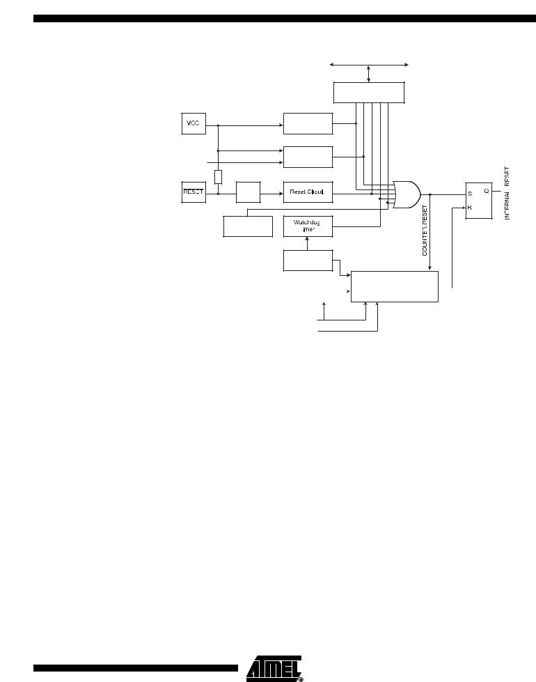
Figure 20. |
Reset Logic |
|
|
|
|
|
|
|
|
DATA BUS |
|
||
|
|
|
MCU Status |
|||
|
|
|
Register (MCUSR) |
|||
|
|
Power-on Reset |
PORF |
BORF EXTRF |
WDRF |
USBRF |
|
|
Circuit |
|
|
|
|
BODLEVEL [2..0] |
Brown-out |
|
|
|
|
|
Reset Circuit |
|
|
|
|
||
|
|
|
|
|
|
|
|
Pull-up Resistor |
|
|
|
|
|
|
SPIKE |
|
|
|
|
|
|
FILTER |
|
|
|
|
|
|
USB Device |
|
|
|
|
|
|
Reset Detection |
|
|
|
|
|
Watchdog
Oscillator
Clock |
CK |
Delay Counters |
|
|
|
||||
Generator |
|
|
TIMEOUT |
|
|
|
|
|
|
CKSEL[3:0]
SUT[1:0]
Table 15. Reset Characteristics(1)
Symbol |
|
Parameter |
Condition |
Min |
Typ |
Max |
Units |
|||
|
|
|
|
|
|
|
|
|||
|
|
Power-on Reset Threshold |
|
TBD |
TBD |
TBD |
V |
|||
|
|
Voltage (rising) |
|
|||||||
VPOT |
|
|
|
|
|
|
||||
|
|
|
|
|
|
|
|
|
|
|
|
Power-on Reset Threshold |
|
TBD |
TBD |
TBD |
V |
||||
|
|
|
||||||||
|
|
Voltage (falling)(2) |
|
|||||||
|
|
|
|
|
|
|
||||
VRST |
|
|
Pin Threshold Voltage |
|
TBD |
TBD |
TBD |
V |
||
|
RESET |
|
||||||||
|
|
Minimum pulse width on |
|
|
|
|
|
|
|
|
tRST |
|
RESET |
|
|
TBD |
TBD |
TBD |
ns |
||
|
Pin |
|
||||||||
Notes: 1. Values are guidelines only. Actual values are TBD.
|
2. The Power-on Reset will not work unless the supply voltage has been below VPOT (falling) |
Power-on Reset |
A Power-on Reset (POR) pulse is generated by an On-chip detection circuit. The detection level |
|
is defined in Table 15. The POR is activated whenever VCC is below the detection level. The |
|
POR circuit can be used to trigger the start-up Reset, as well as to detect a failure in supply |
|
voltage. |
A Power-on Reset (POR) circuit ensures that the device is reset from Power-on. Reaching the Power-on Reset threshold voltage invokes the delay counter, which determines how long the device is kept in RESET after VCC rise. The RESET signal is activated again, without any delay, when VCC decreases below the detection level.
47
7707A–AVR–01/07
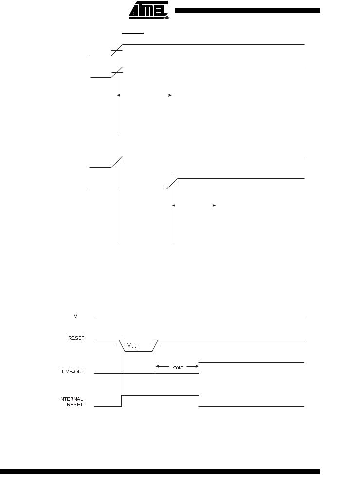
Figure 21. MCU Start-up, RESET Tied to VCC
|
|
VCC |
VPOT |
||||||||||||||||||
|
|
|
|
|
|
|
|
|
|
|
|
|
|
|
|
||||||
|
|
|
|
|
|
|
|
VRST |
|||||||||||||
|
|
RESET |
|||||||||||||||||||
|
|
|
|
|
|
|
|
|
|
|
|
|
|
|
|
||||||
|
TIME-OUT |
|
|
|
|
tTOUT |
|
|
|
|
|
|
|
|
|
||||||
|
|
|
|
|
|
|
|
|
|
|
|
|
|||||||||
|
|
|
|
|
|
|
|
|
|
|
|
|
|
|
|||||||
|
|
|
|
|
|
|
|
|
|
|
|
|
|
|
|
|
|
|
|||
|
INTERNAL |
|
|
|
|
|
|
|
|
|
|
|
|
|
|
|
|
||||
|
RESET |
|
|
|
|
|
|
|
|
|
|
|
|
|
|
|
|
|
|||
|
Figure 22. MCU Start-up, |
|
|
Extended Externally |
|||||||||||||||||
|
RESET |
||||||||||||||||||||
|
|
VCC |
VPOT |
||||||||||||||||||
|
|
|
|
|
|
|
|
|
|
|
|
|
|
|
|
||||||
|
|
|
|
|
|
|
|
|
|
|
|
|
|
VRST |
|||||||
|
|
RESET |
|
|
|
|
|
||||||||||||||
|
|
|
|
|
|
|
|
|
|
|
|
|
|
|
|
||||||
|
TIME-OUT |
|
|
|
|
|
|
|
|
tTOUT |
|
|
|
|
|||||||
|
|
|
|
|
|
|
|
|
|
|
|||||||||||
|
|
|
|
|
|
|
|
|
|
|
|||||||||||
|
|
|
|
|
|
|
|
|
|
|
|
|
|
|
|||||||
|
|
|
|
|
|
|
|
|
|
|
|
|
|
|
|
||||||
|
INTERNAL |
|
|
|
|
|
|
|
|
|
|
|
|
|
|
|
|
||||
External Reset |
RESET |
|
|
|
|
|
|
|
|
|
|
|
|
|
|
|
|
||||
An External Reset is generated by a low level on the |
|
|
|
|
pin. Reset pulses longer than the |
||||||||||||||||
RESET |
|||||||||||||||||||||
|
minimum pulse width (see Table 15) will generate a reset, even if the clock is not running. |
||||||||||||||||||||
|
Shorter pulses are not guaranteed to generate a reset. When the applied signal reaches the |
||||||||||||||||||||
Reset Threshold Voltage – VRST – on its positive edge, the delay counter starts the MCU after the Time-out period – tTOUT – has expired.
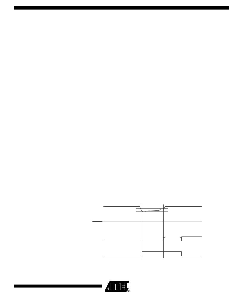
Figure 23. External Reset During Operation
CC
Brown-out Detection AT90USB82/162 has an On-chip Brown-out Detection (BOD) circuit for monitoring the VCC level during operation by comparing it to a fixed trigger level. The trigger level for the BOD can be selected by the BODLEVEL Fuses. The trigger level has a hysteresis to ensure spike free
48
7707A–AVR–01/07
Brown-out Detection. The hysteresis on the detection level should be interpreted as VBOT+ =
VBOT + VHYST/2 and VBOT- = VBOT - VHYST/2.
Table 16. BODLEVEL Fuse Coding(1)
BODLEVEL 2..0 Fuses |
Min VBOT |
Typ VBOT |
Max VBOT |
Units |
111 |
|
BOD Disabled |
|
|
|
|
|
|
|
110 |
|
2.7 |
|
|
|
|
|
|
|
101 |
|
2.9 |
|
|
|
|
|
|
|
100 |
|
3.0 |
|
|
|
|
|
|
|
011 |
|
3.5 |
|
V |
|
|
|
|
|
010 |
|
3.6 |
|
|
|
|
|
|
|
001 |
|
4.0 |
|
|
|
|
|
|
|
000 |
|
4.3 |
|
|
|
|
|
|
|
Note: 1. VBOT may be below nominal minimum operating voltage for some devices. For devices where this is the case, the device is tested down to VCC = VBOT during the production test. This guarantees that a Brown-Out Reset will occur before VCC drops to a voltage where correct operation of the microcontroller is no longer guaranteed. The test is performed using BODLEVEL = 110 for AT90USB82/162 and BODLEVEL = 101 for AT90USB82/162L.
Table 17. Brown-out Characteristics
Symbol |
Parameter |
Min |
Typ |
Max |
Units |
|
|
|
|
|
|
VHYST |
Brown-out Detector Hysteresis |
|
50 |
|
mV |
tBOD |
Min Pulse Width on Brown-out Reset |
|
|
|
ns |
When the BOD is enabled, and VCC decreases to a value below the trigger level (VBOT- in Figure 24), the Brown-out Reset is immediately activated. When VCC increases above the trigger level
(VBOT+ in Figure 24), the delay counter starts the MCU after the Time-out period tTOUT has expired.
The BOD circuit will only detect a drop in VCC if the voltage stays below the trigger level for longer than tBOD given in Table 15.
Figure 24. Brown-out Reset During Operation
VCC |
VBOT+ |
|
VBOT- |
RESET |
|
TIME-OUT |
tTOUT |
INTERNAL |
|
RESET |
|
49
7707A–AVR–01/07