

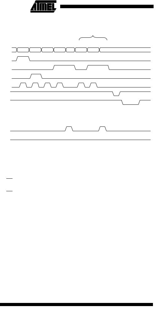
Figure 138. Programming the EEPROM Waveforms
|
|
|
|
|
|
|
|
|
|
|
|
|
|
K |
|
|
|
|
|
|
|
|
|
|
|
A |
G |
B |
C |
E |
B |
C |
E |
L |
|
|
|
|
DATA |
$10 |
ADDR. HIGH ADDR. LOW |
DATA |
XX |
ADDR. LOW |
DATA |
XX |
|
|
|||||
|
|
|
|
|
|
|
|
|
|
|
|
|
|||||
|
|
|
|
XA1 |
|
|
|
|
|
|
|
|
|
|
|||
|
|
|
|
XA0 |
|
|
|
|
|
|
|
|
|
|
|||
|
|
|
|
BS1 |
|
|
|
|
|
|
|
|
|
|
|||
|
|
|
XTAL1 |
|
|
|
|
|
|
|
|
|
|
||||
|
|
|
|
|
|
|
|
|
|
|
|
|
|
|
|
|
|
|
|
|
|
|
WR |
|
|
|
|
|
|
|
|
|
|
||
|
|
|
|
|
|
|
|
|
|
|
|
|
|
|
|
|
|
|
|
RDY/BSY |
|
|
|
|
|
|
|
|
|
|
|
||||
|
|
|
|
|
|
|
|
|
|
|
|
|
|
|
|
|
|
|
|
|
|
|
|
|
|
|
|
|
|
|
|||||
|
|
RESET |
+12V |
|
|
|
|
|
|
|
|
|
|
||||
|
|
|
|
|
|
|
|
|
|
|
|
|
|
|
|
|
|
|
|
|
|
|
|
|
|
|
|
|
|
|
|
|
|
||
|
|
|
|
|
|
OE |
|
|
|
|
|
|
|
|
|
|
|
|
|
PAGEL |
|
|
|
|
|
|
|
|
|
|
|||||
|
|
|
|
BS2 |
|
|
|
|
|
|
|
|
|
|
|||
Reading the Flash |
The algorithm for reading the Flash memory is as follows (refer to “Programming the |
||||||||||||||||
|
Flash” on page 285 for details on Command and Address loading): |
|
|
||||||||||||||
1.A: Load Command “0000 0010”.
2.G: Load Address High Byte ($00 - $FF)
3.B: Load Address Low Byte ($00 - $FF)
4.Set OE to “0”, and BS1 to “0”. The Flash word low byte can now be read at DATA.
5.Set BS1 to “1”. The Flash word high byte can now be read at DATA.
6.Set OE to “1”.
Reading the EEPROM |
The algorithm for reading the EEPROM memory is as follows (refer to “Programming the |
||||||||
|
Flash” on page 285 for details on Command and Address loading): |
||||||||
|
1. |
A: Load Command “0000 0011”. |
|||||||
|
2. |
G: Load Address High Byte ($00 - $FF) |
|||||||
|
3. |
B: Load Address Low Byte ($00 - $FF) |
|||||||
|
4. |
Set |
|
|
|
to “0”, and BS1 to “0”. The EEPROM Data byte can now be read at |
|||
|
OE |
||||||||
|
|
DATA. |
|||||||
|
5. |
Set |
|
|
to “1”. |
||||
|
OE |
||||||||
Programming the Fuse Low |
The algorithm for programming the Fuse Low bits is as follows (refer to “Programming |
||||||||
Bits |
the Flash” on page 285 for details on Command and Data loading): |
||||||||
|
1. |
A: Load Command “0100 0000”. |
|||||||
|
2. |
C: Load Data Low Byte. Bit n = “0” programs and bit n = “1” erases the Fuse bit. |
|||||||
|
3. |
Give |
|
|
|
to go high. |
|||
|
WR |
a negative pulse and wait for RDY/BSY |
|||||||
288 ATmega128(L)
2467B–09/01

|
|
|
|
|
|
|
|
ATmega128(L) |
|
|
|
|
|
|
|
|
|
|
|
|
|
|
|
|
|
|
|
|
The algorithm for programming the Fuse high bits is as follows (refer to “Programming |
||||||
Programming the Fuse High |
||||||||
Bits |
the Flash” on page 285 for details on Command and Data loading): |
|||||||
|
|
1. |
A: Load Command “0100 0000”. |
|||||
|
|
2. |
C: Load Data Low Byte. Bit n = “0” programs and bit n = “1” erases the Fuse bit. |
|||||
|
|
3. |
Set BS1 to '1'. This selects high data byte. |
|||||
|
|
4. |
Give |
|
|
|
to go high. |
|
|
|
WR |
a negative pulse and wait for RDY/BSY |
|||||
|
|
5. |
Set BS1 to '0'. This selects low data byte. |
|||||
Programming the Extended |
The algorithm for programming the Extended Fuse bits is as follows (refer to “Program- |
|||||||
Fuse Bits |
ming the Flash” on page 285 for details on Command and Data loading): |
|||||||
|
|
1. |
A: Load Command “0100 0000”. |
|||||
|
|
2. |
C: Load Data Low Byte. Bit n = “0” programs and bit n = “1” erases the Fuse bit. |
|||||
|
|
3. |
Set BS2 to “1” and BS1 to “0”. This selects extended data byte. |
|||||
|
|
4. |
Give |
|
|
|
to go high. |
|
|
|
WR |
a negative pulse and wait for RDY/BSY |
|||||
|
|
5. |
Set BS2 to “0”. This selects low data byte. |
|||||
Programming the Lock Bits The algorithm for programming the Lock bits is as follows (refer to “Programming the Flash” on page 285 for details on Command and Data loading):
1.A: Load Command “0010 0000”.
2.C: Load Data Low Byte. Bit n = “0” programs the Lock bit.
3.Give WR a negative pulse and wait for RDY/BSY to go high.
The Lock bits can only be cleared by executing Chip Erase.
Reading the Fuse and Lock |
The algorithm for reading the Fuse and Lock bits is as follows (refer to “Programming |
||||||
Bits |
the Flash” on page 285 for details on Command loading): |
||||||
|
1. |
A: Load Command “0000 0100”. |
|||||
|
2. |
Set |
|
|
|
|
to “0”, BS2 to “0” and BS1 to “0”. The status of the Fuse Low bits can |
|
OE |
||||||
|
|
now be read at DATA (“0” means programmed). |
|||||
|
3. |
Set |
|
|
|
to “0”, BS2 to “1” and BS1 to “1”. The status of the Fuse High bits can |
|
|
OE |
||||||
|
|
now be read at DATA (“0” means programmed). |
|||||
|
4. |
Set |
|
|
|
to “0”, BS2 to “1” and BS1 to “0”. The status of the Extended Fuse bits |
|
|
OE |
||||||
|
|
can now be read at DATA (“0” means programmed). |
|||||
|
5. |
Set |
|
to “0”, BS2 to “0” and BS1 to “1”. The status of the Lock bits can now be |
|||
|
OE |
||||||
|
|
read at DATA (“0” means programmed). |
|||||
|
6. |
Set |
|
to “1”. |
|||
|
OE |
||||||
289
2467B–09/01
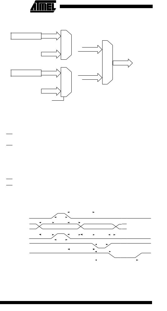
Figure 139. Mapping Between BS1, BS2 and the Fuseand Lock Bits During Read
Fuse Low Byte |
0 |
|
|
|
|
|
|||
|
|
||||||||
|
|
|
|
|
|
0 |
|||
|
|
|
|
|
|
||||
Extended Fuse byte |
1 |
|
|
|
|
|
|||
|
BS2 |
|
|
|
|
|
|
DATA |
|
|
|
|
|
|
|
|
|||
|
|
|
|||||||
|
|
|
|||||||
Lock bits |
0 |
|
|
|
|
|
|||
|
|
|
|
|
|
|
|
||
|
|
|
|
|
1 |
||||
|
|
|
|
|
|
BS1 |
|
||
|
|
|
|
|
|
|
|||
|
|
|
|
|
|
|
|||
Fuse high byte |
1 |
||||||||
|
|
|
|
|
|||||
|
|
|
|
|
|||||
|
|
|
|
|
|
|
|
|
|
BS2
Reading the Signature Bytes The algorithm for reading the Signature bytes is as follows (refer to Programming the Flash for details on Command and Address loading):
1.A: Load Command “0000 1000”.
2.B: Load Address Low Byte ($00 - $02).
3.Set OE to “0”, and BS1 to “0”. The selected Signature byte can now be read at DATA.
4.Set OE to “1”.
Reading the Calibration Byte The algorithm for reading the Calibration byte is as follows (refer to Programming the Flash for details on Command and Address loading):
1.A: Load Command “0000 1000”.
2.B: Load Address Low Byte, $00.
3.Set OE to “0”, and BS1 to “1”. The Calibration byte can now be read at DATA.
4.Set OE to “1”.
Parallel Programming |
Figure 140. Parallel Programming Timing, Including some General Timing |
||||||||||||||||||||||||||||
Characteristics |
Requirements |
|
|
|
|
|
|
|
|
|
|
|
|
|
|
|
|
|
|
|
|
|
|
||||||
|
|
|
|
|
|
|
|
|
|
|
|
tXLWL |
|
|
|
|
|
|
|
|
|
|
|
|
|
|
|
|
|
|
XTAL1 |
|
tXHXL |
|
|
|
|
|
|
|
|
|
|
|
|
|
|
|
|
|
|
|
|||||||
|
|
|
|
|
|
|
|
|
|
|
|
|
|
|
|
|
|
|
|
|
|
|
|||||||
|
Data & Contol |
|
tDVXH |
|
|
|
|
tXLDX |
|
|
|
|
|
|
|
|
|
|
|
|
|
|
|
|
|||||
|
|
|
|
|
|
|
|
|
|
|
|
|
|
|
|
|
|
|
|
|
|
|
|
|
|
||||
|
|
|
|
|
|
|
|
|
|
|
|
|
|
|
|
|
|
|
|
|
|
|
|
|
|
||||
|
(DATA, XA0/1, BS1, BS2) |
|
|
|
|
|
|
|
|
|
|
|
|
|
|
|
|
|
|
|
|
|
|
|
|
|
|||
|
|
|
|
|
|
tBVPH |
|
|
|
|
tPLBX |
|
t BVWL |
|
|
|
|
|
|
|
|
tWLBX |
|
|
|||||
|
|
|
|
|
|
|
|
|
|
|
|
|
|
|
|
|
|
|
|
|
|
|
|
|
|
|
|||
|
PAGEL |
|
tPHPL |
|
|
|
|
|
|
tWL WH |
|
|
|
|
|
|
|
|
|
|
|||||||||
|
|
|
|
|
|
|
|
|
|
|
|
|
|
|
|
|
|
|
|
|
|
|
|
|
|
|
|||
|
|
WR |
|
|
|
|
tPLWL |
|
|
|
|
|
|
|
|
|
|
|
|
|
|
|
|
||||||
|
|
|
|
|
|
|
|
|
|
|
|
|
|
|
WLRL |
|
|
|
|
|
|
|
|||||||
|
|
|
|
|
|
|
|
|
|
|
|
|
|
|
|
|
|
|
|
|
|
|
|
|
|||||
|
|
|
|
|
|
|
|
|
|
|
|
|
|
|
|
|
|
|
|
|
|
|
|
|
|
|
|
|
|
|
RDY/BSY |
|
|
|
|
|
|
|
|
|
|
|
|
|
|
|
|
|
|
|
|
|
|
||||||
|
|
|
|
|
|
|
|
|
|
|
|
|
|
|
|
|
|
|
|
|
|
|
|
|
|
|
|
tWLRH |
|
|
|
|
|
|
|
|
|
|
|
|
|
|
|
|
|
|
|
|
|
|
|
|
|
|
|
|
|
||
|
|
|
|
|
|
|
|
|
|
|
|
|
|
|
|
|
|
|
|
|
|
|
|
|
|
|
|
|
|
290 ATmega128(L)
2467B–09/01
 ATmega128(L)