

- •1. Pin Configurations
- •1.1 Disclaimer
- •2. Overview
- •2.1 Block Diagram
- •2.2 Pin Descriptions
- •2.2.3 Port B (PB3...PB0)
- •2.2.4 RESET
- •2.2.5 Port A (PA7...PA0)
- •3. Resources
- •4. About Code Examples
- •5. CPU Core
- •5.1 Overview
- •5.2 Architectural Overview
- •5.4 Status Register
- •5.5 General Purpose Register File
- •5.6 Stack Pointer
- •5.7 Instruction Execution Timing
- •5.8 Reset and Interrupt Handling
- •5.8.1 Interrupt Response Time
- •6. Memories
- •6.2 SRAM Data Memory
- •6.2.1 Data Memory Access Times
- •6.3 EEPROM Data Memory
- •6.3.1 EEPROM Read/Write Access
- •6.3.2 Atomic Byte Programming
- •6.3.3 Split Byte Programming
- •6.3.4 Erase
- •6.3.5 Write
- •6.3.6 Preventing EEPROM Corruption
- •6.4 I/O Memory
- •6.4.1 General Purpose I/O Registers
- •6.5 Register Description
- •7. System Clock and Clock Options
- •7.1 Clock Systems and their Distribution
- •7.2 Clock Sources
- •7.3 Default Clock Source
- •7.4 Crystal Oscillator
- •7.6 Calibrated Internal RC Oscillator
- •7.7 External Clock
- •7.8 128 kHz Internal Oscillator
- •7.9 System Clock Prescaler
- •7.9.1 Switching Time
- •7.10 Register Description
- •8. Power Management and Sleep Modes
- •8.1 Sleep Modes
- •8.2 Idle Mode
- •8.3 ADC Noise Reduction Mode
- •8.5 Standby Mode
- •8.6 Power Reduction Register
- •8.7 Minimizing Power Consumption
- •8.7.1 Analog to Digital Converter
- •8.7.2 Analog Comparator
- •8.7.4 Internal Voltage Reference
- •8.7.5 Watchdog Timer
- •8.7.6 Port Pins
- •8.8 Register Description
- •9. System Control and Reset
- •9.0.1 Resetting the AVR
- •9.0.2 Reset Sources
- •9.0.3 Power-on Reset
- •9.0.4 External Reset
- •9.0.6 Watchdog Reset
- •9.1 Internal Voltage Reference
- •9.2 Watchdog Timer
- •9.3 Timed Sequences for Changing the Configuration of the Watchdog Timer
- •9.3.1 Safety Level 1
- •9.3.2 Safety Level 2
- •9.4 Register Description
- •10. Interrupts
- •10.1 Interrupt Vectors
- •11. External Interrupts
- •11.1 Pin Change Interrupt Timing
- •11.2 Register Description
- •12. I/O Ports
- •12.1 Overview
- •12.2 Ports as General Digital I/O
- •12.2.1 Configuring the Pin
- •12.2.2 Toggling the Pin
- •12.2.3 Switching Between Input and Output
- •12.2.4 Reading the Pin Value
- •12.2.5 Digital Input Enable and Sleep Modes
- •12.2.6 Unconnected Pins
- •12.3 Alternate Port Functions
- •12.3.1 Alternate Functions of Port A
- •12.3.2 Alternate Functions of Port B
- •12.4 Register Description
- •13. 8-bit Timer/Counter0 with PWM
- •13.1 Features
- •13.2 Overview
- •13.2.1 Registers
- •13.2.2 Definitions
- •13.3 Timer/Counter Clock Sources
- •13.4 Counter Unit
- •13.5 Output Compare Unit
- •13.5.1 Force Output Compare
- •13.5.2 Compare Match Blocking by TCNT0 Write
- •13.5.3 Using the Output Compare Unit
- •13.6 Compare Match Output Unit
- •13.6.1 Compare Output Mode and Waveform Generation
- •13.7 Modes of Operation
- •13.7.1 Normal Mode
- •13.7.2 Clear Timer on Compare Match (CTC) Mode
- •13.7.3 Fast PWM Mode
- •13.7.4 Phase Correct PWM Mode
- •13.8 Timer/Counter Timing Diagrams
- •13.9 Register Description
- •14. 16-bit Timer/Counter1
- •14.1 Features
- •14.2 Overview
- •14.2.1 Registers
- •14.2.2 Definitions
- •14.2.3 Compatibility
- •14.3.1 Reusing the Temporary High Byte Register
- •14.4 Timer/Counter Clock Sources
- •14.5 Counter Unit
- •14.6 Input Capture Unit
- •14.6.1 Input Capture Trigger Source
- •14.6.2 Noise Canceler
- •14.6.3 Using the Input Capture Unit
- •14.7 Output Compare Units
- •14.7.1 Force Output Compare
- •14.7.2 Compare Match Blocking by TCNT1 Write
- •14.7.3 Using the Output Compare Unit
- •14.8 Compare Match Output Unit
- •14.8.1 Compare Output Mode and Waveform Generation
- •14.9 Modes of Operation
- •14.9.1 Normal Mode
- •14.9.2 Clear Timer on Compare Match (CTC) Mode
- •14.9.3 Fast PWM Mode
- •14.9.4 Phase Correct PWM Mode
- •14.9.5 Phase and Frequency Correct PWM Mode
- •14.10 Timer/Counter Timing Diagrams
- •14.11 Register Description
- •15. Timer/Counter Prescaler
- •15.0.1 Prescaler Reset
- •15.0.2 External Clock Source
- •15.1 Register Description
- •16.1 Features
- •16.2 Overview
- •16.3 Functional Descriptions
- •16.3.2 SPI Master Operation Example
- •16.3.3 SPI Slave Operation Example
- •16.3.5 Start Condition Detector
- •16.3.6 Clock speed considerations
- •16.4 Alternative USI Usage
- •16.4.4 Edge Triggered External Interrupt
- •16.4.5 Software Interrupt
- •16.5 Register Descriptions
- •17. Analog Comparator
- •17.1 Analog Comparator Multiplexed Input
- •17.2 Register Description
- •18. Analog to Digital Converter
- •18.1 Features
- •18.2 Overview
- •18.3 ADC Operation
- •18.4 Starting a Conversion
- •18.5 Prescaling and Conversion Timing
- •18.6 Changing Channel or Reference Selection
- •18.6.1 ADC Input Channels
- •18.6.2 ADC Voltage Reference
- •18.7 ADC Noise Canceler
- •18.7.1 Analog Input Circuitry
- •18.7.2 Analog Noise Canceling Techniques
- •18.7.3 ADC Accuracy Definitions
- •18.8 ADC Conversion Result
- •18.8.1 Single Ended Conversion
- •18.8.2 Unipolar Differential Conversion
- •18.8.3 Bipolar Differential Conversion
- •18.9 Temperature Measurement
- •18.10 Register Description
- •18.10.3.1 ADLAR = 0
- •18.10.3.2 ADLAR = 1
- •19. debugWIRE On-chip Debug System
- •19.1 Features
- •19.2 Overview
- •19.3 Physical Interface
- •19.4 Software Break Points
- •19.5 Limitations of debugWIRE
- •19.6 Register Description
- •20. Self-Programming the Flash
- •20.0.1 Performing Page Erase by SPM
- •20.0.2 Filling the Temporary Buffer (Page Loading)
- •20.0.3 Performing a Page Write
- •20.1.1 EEPROM Write Prevents Writing to SPMCSR
- •20.1.2 Reading the Fuse and Lock Bits from Software
- •20.1.3 Preventing Flash Corruption
- •20.1.4 Programming Time for Flash when Using SPM
- •20.2 Register Description
- •21. Memory Programming
- •21.1 Program And Data Memory Lock Bits
- •21.2 Fuse Bytes
- •21.2.1 Latching of Fuses
- •21.3 Signature Bytes
- •21.4 Calibration Byte
- •21.5 Page Size
- •21.6 Serial Downloading
- •21.6.1 Serial Programming Algorithm
- •21.6.2 Serial Programming Instruction set
- •21.7 High-voltage Serial Programming
- •21.8.2 Considerations for Efficient Programming
- •21.8.3 Chip Erase
- •21.8.4 Programming the Flash
- •21.8.5 Programming the EEPROM
- •21.8.6 Reading the Flash
- •21.8.7 Reading the EEPROM
- •21.8.8 Programming and Reading the Fuse and Lock Bits
- •21.8.9 Reading the Signature Bytes and Calibration Byte
- •22. Electrical Characteristics
- •22.1 Absolute Maximum Ratings*
- •22.2 Speed Grades
- •22.3 Clock Characterizations
- •22.3.1 Calibrated Internal RC Oscillator Accuracy
- •22.3.2 External Clock Drive Waveforms
- •22.3.3 External Clock Drive
- •22.4 System and Reset Characterizations
- •22.6 Serial Programming Characteristics
- •22.7 High-voltage Serial Programming Characteristics
- •23.1 Active Supply Current
- •23.2 Idle Supply Current
- •23.3 Supply Current of IO modules
- •23.3.0.1 Example 1
- •23.5 Standby Supply Current
- •23.7 Pin Driver Strength
- •23.8 Pin Threshold and Hysteresis
- •23.9 BOD Threshold and Analog Comparator Offset
- •23.10 Internal Oscillator Speed
- •23.11 Current Consumption of Peripheral Units
- •23.12 Current Consumption in Reset and Reset Pulsewidth
- •24. Register Summary
- •25. Instruction Set Summary
- •26. Ordering Information
- •26.1 ATtiny24
- •26.2 ATtiny44
- •26.3 ATtiny84
- •27. Packaging Information
- •28. Errata
- •28.1 ATtiny24
- •28.2 ATtiny44
- •28.3 ATtiny84
- •29. Datasheet Revision History
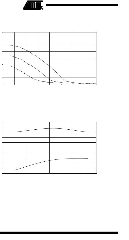
Figure 23-29. Reset Pin Input Hysteresis vs. VCC
RESET PIN INPUT HYSTERESIS vs. VCC
|
0.8 |
|
|
|
|
|
|
|
|
|
0.7 |
|
|
|
|
|
|
|
|
(mV) |
0.6 |
|
|
|
|
|
|
|
|
|
|
|
|
|
|
|
|
|
|
Hysteresis |
0.5 |
|
|
|
|
|
|
|
|
0.4 |
|
|
|
|
|
|
|
|
|
|
|
|
|
|
|
|
|
|
|
Input |
0.3 |
|
|
|
|
|
|
|
|
|
|
|
|
|
|
|
|
|
|
|
0.2 |
|
|
|
|
|
|
|
-40 ˚C |
|
|
|
|
|
|
|
|
|
|
|
0.1 |
|
|
|
|
|
|
|
25 ˚C |
|
0 |
|
|
|
|
|
|
|
85 ˚C |
|
|
|
|
|
|
|
|
|
|
|
1.5 |
2 |
2.5 |
3 |
3.5 |
4 |
4.5 |
5 |
5.5 |
VCC (V)
23.9BOD Threshold and Analog Comparator Offset
Figure 23-30. BOD Threshold vs. Temperature (BODLEVEL is 4.3V)
BOD THRESHOLDS vs. TEMPERATURE
Threshold (V)
BODLEVEL is 4.3V
4.34
4.32
Rising Vcc
4.3
4.28
4.26
4.24
4.22
Falling Vcc
4.2
4.18
4.16
4.14
-60 |
-40 |
-20 |
0 |
20 |
40 |
60 |
80 |
100 |
Temperature (C)
204 ATtiny24/44/84
8006E–AVR–09/06

ATtiny24/44/84
Figure 23-31. BOD Threshold vs, Temperature (BODLEVEL is 2.7V)
BOD THRESHOLDS vs. TEMPERATURE
BODLEVEL is 2.7V
Threshold (V)
2.75
2.74 Rising Vcc
2.73
2.72
2.71
2.7
2.69
2.68
2.67
Falling Vcc
2.66
2.65
2.64
-60 |
-40 |
-20 |
0 |
20 |
40 |
60 |
80 |
100 |
Temperature (C)
Figure 23-32. BOD Threshold vs. Temperature (BODLEVEL is 1.8V)
BOD THRESHOLDS vs. TEMPERATURE
Threshold (V)
1.82 |
|
|
|
|
|
|
|
|
BODLEVEL is 1.8V |
|
|
|
|
|
|
|||
|
|
|
|
|
|
|
|
|
|
|
|
|
|
Rising |
Vcc |
|
|
|
1.815 |
|
|
|
|
|
|
|
|
|
|
|
|
|
|
|
|
||
|
|
|
|
|
|
|
|
|
|
|
|
|
|
|
|
|
||
1.81 |
|
|
|
|
|
|
|
|
|
|
|
|
|
|
|
|
|
|
|
|
|
|
|
|
|
|
|
|
|
|
|
|
|
|
|
||
1.805 |
|
|
|
|
|
|
|
|
|
|
|
|
|
|
|
|
|
|
|
|
|
|
|
|
|
|
|
|
|
|
|
|
|
|
|
||
1.8 |
|
|
|
|
|
|
|
|
|
|
|
|
|
|
|
|
|
|
|
|
|
|
|
|
|
|
|
|
|
|
|
|
|
|
|
||
1.795 |
|
|
|
|
|
|
|
|
|
|
|
|
|
|
|
|
|
|
|
|
|
|
|
|
|
|
|
|
|
|
|
|
|
|
|
||
1.79 |
|
|
|
|
|
|
|
|
|
|
|
|
|
|
|
|
|
|
|
|
|
|
|
|
|
|
|
|
|
|
|
Falling |
Vcc |
|
|
||
1.785 |
|
|
|
|
|
|
|
|
|
|
|
|
|
|
|
|
||
|
|
|
|
|
|
|
|
|
|
|
|
|
|
|
|
|
||
1.78 |
|
|
|
|
|
|
|
|
|
|
|
|
|
|
|
|
|
|
|
|
|
|
|
|
|
|
|
|
|
|
|
|
|
|
|
||
1.775 |
|
|
|
|
|
|
|
|
|
|
|
|
|
|
|
|
|
|
|
|
|
|
|
|
|
|
|
|
|
|
|
|
|
|
|
||
1.77 |
|
|
|
|
|
|
|
|
|
|
|
|
|
|
|
|
|
|
|
|
|
|
|
|
|
|
|
|
|
|
|
|
|
|
|
|
|
-60 |
-40 |
-20 |
0 |
20 |
40 |
60 |
80 |
100 |
||||||||||
Temperature (C)
205
8006E–AVR–09/06

23.10 Internal Oscillator Speed
Figure 23-33. Watchdog Oscillator Frequency vs. VCC
WATCHDOG OSCILLATOR FREQUENCY vs. VCC
|
108 |
|
|
|
|
|
|
|
|
|
107 |
|
|
|
|
|
|
|
|
|
106 |
|
|
|
|
|
|
|
|
|
105 |
|
|
|
|
|
|
|
-40 ˚C |
(kHz) |
104 |
|
|
|
|
|
|
|
|
103 |
|
|
|
|
|
|
|
25 ˚C |
|
|
|
|
|
|
|
|
|
||
RC |
102 |
|
|
|
|
|
|
|
|
F |
|
|
|
|
|
|
|
|
|
|
101 |
|
|
|
|
|
|
|
|
|
100 |
|
|
|
|
|
|
|
|
|
99 |
|
|
|
|
|
|
|
|
|
98 |
|
|
|
|
|
|
|
85 ˚C |
|
|
|
|
|
|
|
|
|
|
|
97 |
|
|
|
|
|
|
|
|
|
1.5 |
2 |
2.5 |
3 |
3.5 |
4 |
4.5 |
5 |
5.5 |
VCC (V)
Figure 23-34. Watchdog Oscillator Frequency vs. Temperature
WATCHDOG OSCILLATOR FREQUENCY vs. TEMPERATURE
FRC(kHz)
108 |
|
|
|
|
|
|
|
|
|
|
|
|
|
|
|
|
|
|
|
|
|
|
|
|
|
|
|
|
|
|
|
|
|
|
|
||
107 |
|
|
|
|
|
|
|
|
|
|
|
|
|
|
|
|
|
|
|
|
|
|
|
|
|
|
|
|
|
|
|
|
|
|
|
||
106 |
|
|
|
|
|
|
|
|
|
|
|
|
|
|
|
|
|
|
|
|
|
|
|
|
|
|
|
|
|
|
|
|
|
|
|
||
105 |
|
|
|
|
|
|
|
|
|
|
|
|
|
|
|
|
|
|
|
|
|
|
|
|
|
|
|
|
|
|
|
|
|
|
|
||
104 |
|
|
|
|
|
|
|
|
|
|
|
|
|
|
|
|
|
|
|
|
|
|
|
|
|
|
|
|
|
|
|
|
|
|
|
||
103 |
|
|
|
|
|
|
|
|
|
|
|
|
|
|
|
|
|
|
|
|
|
|
|
|
|
|
|
|
|
|
|
|
|
|
|
||
102 |
|
|
|
|
|
|
|
|
|
|
|
|
|
|
|
|
|
|
|
|
|
|
|
|
|
|
|
|
|
|
|
|
|
2.1 V |
|
||
101 |
|
|
|
|
|
|
|
|
|
|
|
|
|
|
|
|
|
|
|
|
|
|
|
|
|
|
|
|
|
|
|
|
|
|
2.7 V |
|
|
100 |
|
|
|
|
|
|
|
|
|
|
|
|
|
|
|
|
|
|
|
|
|
|
|
|
|
|
|
|
|
|
|
|
|
|
3.3 V |
|
|
|
|
|
|
|
|
|
|
|
|
|
|
|
|
|
|
|
|
|
99 |
|
|
|
|
|
|
|
|
|
|
|
|
|
|
|
|
4.0 V |
|
98 |
|
|
|
|
|
|
|
|
|
|
|
|
|
|
|
|
5.5 V |
|
|
|
|
|
|
|
|
|
|
|
|
|
|
|
|
|
|
|
|
97 |
|
|
|
|
|
|
|
|
|
|
|
|
|
|
|
|
|
|
|
|
|
|
|
|
|
|
|
|
|
|
|
|
|
|
|
|
|
-60 |
-40 |
-20 |
0 |
20 |
40 |
60 |
80 |
100 |
||||||||||
Temperature
206 ATtiny24/44/84
8006E–AVR–09/06

 ATtiny24/44/84
Figure 23-35. Calibrated 8 MHz RC Oscillator Frequency vs. VCC
CALIBRATED 8 MHz RC OSCILLATOR FREQUENCY vs. V CC
FRC(MHz)
8.3
8.2 |
85 ˚C |
8.1 |
25 ˚C |
|
|
8 |
|
7.9
 -40 ˚C
7.8
7.7
7.6
7.5
1.5 |
2 |
2.5 |
3 |
3.5 |
4 |
4.5 |
5 |
5.5 |
VCC (V)
Figure 23-36. Calibrated 8 MHz RC oscillator Frequency vs. Temperature
CALIBRATED 8 MHz RC OSCILLATOR FREQUENCY vs. TEMPERATURE
FRC(MHz)
8.2
5.0 V
8.15
3.0 V
8.1
8.05
8
7.95
7.9
7.85
7.8
-60 |
-40 |
-20 |
0 |
20 |
40 |
60 |
80 |
100 |
Temperature
207
8006E–AVR–09/06