
- •Features
- •1. Pin Configurations
- •2. Overview
- •2.1 Block Diagram
- •2.2 Automotive Quality Grade
- •2.3 Pin Descriptions
- •2.3.3 Port B (PB5..PB0)
- •2.3.4 RESET
- •3. About Code Examples
- •4. AVR CPU Core
- •4.1 Introduction
- •4.2 Architectural Overview
- •4.4 Status Register
- •4.5 General Purpose Register File
- •4.6 Stack Pointer
- •4.7 Instruction Execution Timing
- •4.8 Reset and Interrupt Handling
- •4.8.1 Interrupt Response Time
- •5. AVR ATtiny25/45/85 Memories
- •5.2 SRAM Data Memory
- •5.2.1 Data Memory Access Times
- •5.3 EEPROM Data Memory
- •5.3.1 EEPROM Read/Write Access
- •5.3.6 Atomic Byte Programming
- •5.3.7 Split Byte Programming
- •5.3.8 Erase
- •5.3.9 Write
- •5.3.10 Preventing EEPROM Corruption
- •5.4 I/O Memory
- •6. System Clock and Clock Options
- •6.1 Clock Systems and their Distribution
- •6.2 Clock Sources
- •6.3 Default Clock Source
- •6.4 Crystal Oscillator
- •6.6 Calibrated Internal RC Oscillator
- •6.7 External Clock
- •6.8 128 kHz Internal Oscillator
- •6.9 Clock Output Buffer
- •6.10 System Clock Prescaler
- •6.10.2 Switching Time
- •7. Power Management and Sleep Modes
- •7.1 Idle Mode
- •7.2 ADC Noise Reduction Mode
- •7.4 Power Reduction Register
- •7.5 Minimizing Power Consumption
- •7.5.1 Analog to Digital Converter
- •7.5.2 Analog Comparator
- •7.5.4 Internal Voltage Reference
- •7.5.5 Watchdog Timer
- •7.5.6 Port Pins
- •8. System Control and Reset
- •8.0.1 Resetting the AVR
- •8.0.2 Reset Sources
- •8.0.3 Power-on Reset
- •8.0.4 External Reset
- •8.0.6 Watchdog Reset
- •8.1 Internal Voltage Reference
- •8.2 Watchdog Timer
- •8.3 Timed Sequences for Changing the Configuration of the Watchdog Timer
- •8.3.1 Safety Level 1
- •8.3.2 Safety Level 2
- •9. Interrupts
- •9.1 Interrupt Vectors in ATtiny25/45/85
- •10. I/O Ports
- •10.1 Introduction
- •10.2 Ports as General Digital I/O
- •10.2.1 Configuring the Pin
- •10.2.2 Toggling the Pin
- •10.2.3 Switching Between Input and Output
- •10.2.4 Reading the Pin Value
- •10.2.5 Digital Input Enable and Sleep Modes
- •10.2.6 Unconnected Pins
- •10.3 Alternate Port Functions
- •10.3.2 Alternate Functions of Port B
- •11. External Interrupts
- •12. 8-bit Timer/Counter0 with PWM
- •12.1 Overview
- •12.1.1 Registers
- •12.1.2 Definitions
- •12.2 Timer/Counter Clock Sources
- •12.3 Counter Unit
- •12.4 Output Compare Unit
- •12.4.1 Force Output Compare
- •12.4.2 Compare Match Blocking by TCNT0 Write
- •12.4.3 Using the Output Compare Unit
- •12.5 Compare Match Output Unit
- •12.5.1 Compare Output Mode and Waveform Generation
- •12.6 Modes of Operation
- •12.6.1 Normal Mode
- •12.6.2 Clear Timer on Compare Match (CTC) Mode
- •12.6.3 Fast PWM Mode
- •12.6.4 Phase Correct PWM Mode
- •12.7 Timer/Counter Timing Diagrams
- •13. Timer/Counter Prescaler
- •13.0.1 Prescaler Reset
- •13.0.2 External Clock Source
- •14. 8-bit Timer/Counter1
- •14.1 Timer/Counter1
- •14.1.1 Timer/Counter1 Control Register - TCCR1
- •14.1.2 General Timer/Counter1 Control Register - GTCCR
- •14.1.3 Timer/Counter1 - TCNT1
- •14.1.4 Timer/Counter1 Output Compare RegisterA - OCR1A
- •14.1.5 Timer/Counter1 Output Compare RegisterB - OCR1B
- •14.1.6 Timer/Counter1 Output Compare RegisterC - OCR1C
- •14.1.7 Timer/Counter Interrupt Mask Register - TIMSK
- •14.1.8 Timer/Counter Interrupt Flag Register - TIFR
- •14.1.9 PLL Control and Status Register - PLLCSR
- •14.1.10 Timer/Counter1 Initialization for Asynchronous Mode
- •14.1.11 Timer/Counter1 in PWM Mode
- •15. 8-bit Timer/Counter1 in ATtiny15 Mode
- •15.1 Timer/Counter1 Prescaler
- •15.2 Timer/Counter1
- •15.2.2 Timer/Counter1 Control Register - TCCR1
- •15.2.3 General Timer/Counter1 Control Register - GTCCR
- •15.2.4 Timer/Counter1 - TCNT1
- •15.2.5 Timer/Counter1 Output Compare RegisterA - OCR1A
- •15.2.6 Timer/Counter1 Output Compare Register C - OCR1C
- •15.2.7 Timer/Counter Interrupt Flag Register - TIFR
- •15.2.8 PLL Control and Status Register - PLLCSR
- •15.2.9 Timer/Counter1 in PWM Mode
- •16. Dead Time Generator
- •16.0.1 Timer/Counter1 Dead Time Prescaler register 1 - DTPS1
- •16.0.2 Timer/Counter1 Dead Time A - DT1A
- •16.0.3 Timer/Counter1 Dead Time B - DT1B
- •17.1 Overview
- •17.2 Functional Descriptions
- •17.2.2 SPI Master Operation Example
- •17.2.3 SPI Slave Operation Example
- •17.2.5 Start Condition Detector
- •17.3 Alternative USI Usage
- •17.3.4 Edge Triggered External Interrupt
- •17.3.5 Software Interrupt
- •17.4 USI Register Descriptions
- •18. Analog Comparator
- •18.1 Analog Comparator Multiplexed Input
- •19. Analog to Digital Converter
- •19.1 Features
- •19.2 Operation
- •19.3 Starting a Conversion
- •19.4 Prescaling and Conversion Timing
- •19.5 Changing Channel or Reference Selection
- •19.5.1 ADC Input Channels
- •19.5.2 ADC Voltage Reference
- •19.6 ADC Noise Canceler
- •19.6.1 Analog Input Circuitry
- •19.6.2 Analog Noise Canceling Techniques
- •19.6.3 ADC Accuracy Definitions
- •19.7 ADC Conversion Result
- •19.7.1 Single Ended Conversion
- •19.7.2 Unipolar Differential Conversion
- •19.7.3 Bipolar Differential Conversion
- •19.7.4 Temperature Measurement (Preliminary description)
- •19.7.7.1 ADLAR = 0
- •19.7.7.2 ADLAR = 1
- •20. debugWIRE On-chip Debug System
- •20.1 Features
- •20.2 Overview
- •20.3 Physical Interface
- •20.4 Software Break Points
- •20.5 Limitations of debugWIRE
- •20.6 debugWIRE Related Register in I/O Memory
- •21. Self-Programming the Flash
- •21.0.1 Performing Page Erase by SPM
- •21.0.2 Filling the Temporary Buffer (Page Loading)
- •21.0.3 Performing a Page Write
- •21.1.2 EEPROM Write Prevents Writing to SPMCSR
- •21.1.3 Reading the Fuse and Lock Bits from Software
- •21.1.4 Preventing Flash Corruption
- •21.1.5 Programming Time for Flash when Using SPM
- •22. Memory Programming
- •22.1 Program And Data Memory Lock Bits
- •22.2 Fuse Bytes
- •22.2.1 Latching of Fuses
- •22.3 Signature Bytes
- •22.3.1 ATtiny25 Signature Bytes
- •22.3.2 ATtiny45 Signature Bytes
- •22.3.3 ATtiny85 Signature Bytes
- •22.4 Calibration Byte
- •22.5 Page Size
- •22.6 Serial Downloading
- •22.6.1 Serial Programming Algorithm
- •22.6.2 Serial Programming Characteristics
- •22.7 High-voltage Serial Programming
- •22.8.2 Considerations for Efficient Programming
- •22.8.3 Chip Erase
- •22.8.4 Programming the Flash
- •22.8.5 Programming the EEPROM
- •22.8.6 Reading the Flash
- •22.8.7 Reading the EEPROM
- •22.8.8 Programming and Reading the Fuse and Lock Bits
- •22.8.9 Reading the Signature Bytes and Calibration Byte
- •23. Electrical Characteristics
- •23.1 Absolute Maximum Ratings*
- •23.2 External Clock Drive Waveforms
- •23.3 External Clock Drive
- •23.5 Calibrated RC Oscillator Accuracy
- •24. Typical Characteristics
- •24.1 Active Supply Current
- •24.2 Idle Supply Current
- •24.2.1 Using the Power Reduction Register
- •24.2.1.1 Example 1
- •24.5 Pin Driver Strength
- •24.6 Pin Thresholds and Hysteresis
- •24.7 BOD Thresholds and Analog Comparator Offset
- •24.8 Internal Oscillator Speed
- •24.9 Current Consumption of Peripheral Units
- •24.10 Current Consumption in Reset and Reset Pulse width
- •24.11 Analog to Digital Converter
- •25. Register Summary
- •26. Instruction Set Summary
- •27. Ordering Information
- •28. Packaging Information
- •29. Document Revision History
- •30. Errata
- •30.1 ATtiny25/45/85 Rev. A

23.5Calibrated RC Oscillator Accuracy
Table 23-3. Calibration Accuracy of Internal RC Oscillator
|
Frequency |
Vcc |
Temperature |
Calibration |
|
|
Accuracy |
||||
|
|
|
|
||
|
|
|
|
|
|
Factory |
8.0 MHz |
3V |
25°C |
±1% |
|
Calibration |
|||||
|
|
|
|
||
|
|
|
|
|
|
User Calibration |
7.3 - 8.1 MHz |
2.7V - 5.5V |
-40°C - +125°C |
±14% |
|
|
|
|
|
|
24. Typical Characteristics
The data contained in this section is extracted from actual silicon characterization and should be treated as indications of how the part will behave.
The following charts show typical behavior. These figures are not tested during manufacturing. All current consumption measurements are performed with all I/O pins configured as inputs and with internal pull-ups enabled. A sine wave generator with railtorail output is used as clock source.
The power consumption in Power-down mode is independent of clock selection.
The current consumption is a function of several factors such as: operating voltage, operating frequency, loading of I/O pins, switching rate of I/O pins, code executed and ambient temperature. The dominating factors are operating voltage and frequency.
The current drawn from capacitive loaded pins may be estimated (for one pin) as CL*VCC*f where CL = load capacitance, VCC = operating voltage and f = average switching frequency of I/O pin.
The parts are characterized at frequencies higher than test limits. Parts are not guaranteed to function properly at frequencies higher than the ordering code indicates.
The difference between current consumption in Power-down mode with Watchdog Timer enabled and Power-down mode with Watchdog Timer disabled represents the differential current drawn by the Watchdog Timer.
160 ATtiny25/45/85 Auto
7598C–AVR–09/06

ATtiny25/45/85 Auto
24.1Active Supply Current
Figure 24-1. Active Supply Current vs. Frequency (0.1 - 1.0 MHz)
ACTIVE S UP P LY CURRENT vs . LOW FREQUENCY
|
|
|
|
|
|
0.1 - 1.0 MHz |
|
|
|
|
|
|
0.040 |
|
|
|
|
|
|
|
|
|
|
|
|
|
|
|
|
|
|
|
|
|
5.5 V |
|
0.035 |
|
|
|
|
|
|
|
|
|
5.0 V |
|
|
|
|
|
|
|
|
|
|
|
|
|
0.030 |
|
|
|
|
|
|
|
|
|
4.5 V |
|
|
|
|
|
|
|
|
|
|
|
|
|
0.025 |
|
|
|
|
|
|
|
|
|
4.0 V |
(mA) |
0.020 |
|
|
|
|
|
|
|
|
|
3.3 V |
CC |
|
|
|
|
|
|
|
|
|
|
|
|
|
|
|
|
|
|
|
|
|
2.7 V |
|
I |
|
|
|
|
|
|
|
|
|
|
|
|
0.015 |
|
|
|
|
|
|
|
|
|
|
|
|
|
|
|
|
|
|
|
|
|
|
|
0.010 |
|
|
|
|
|
|
|
|
|
1.8 V |
|
0.005 |
|
|
|
|
|
|
|
|
|
|
|
0.000 |
|
|
|
|
|
|
|
|
|
|
|
0 |
0.1 |
0.2 |
0.3 |
0.4 |
0.5 |
0.6 |
0.7 |
0.8 |
0.9 |
1 |
Frequency (MHz)
Figure 24-2. Active Supply Current vs. Frequency (1 - 20 MHz)
ACTIVE S UP P LY CURRENT vs . FREQUENCY
|
|
|
|
|
1 - 20MHz |
|
|
|
|
|
14 |
|
|
|
|
|
|
|
|
|
|
|
|
|
|
|
|
|
|
|
|
5.5 V |
12 |
|
|
|
|
|
|
|
|
|
5.0 V |
|
|
|
|
|
|
|
|
|
|
|
10 |
|
|
|
|
|
|
|
|
|
4.5 V |
8 |
|
|
|
|
|
|
|
|
|
|
CC(mA) |
|
|
|
|
|
|
|
|
4.0 V |
|
I |
|
|
|
|
|
|
|
|
|
|
6 |
|
|
|
|
|
|
|
|
|
|
|
|
|
|
|
|
|
|
|
|
|
4 |
|
|
|
|
|
|
3.3 V |
|
|
|
|
|
|
|
|
|
|
|
|
|
|
|
|
|
|
|
2.7 V |
|
|
|
|
|
2 |
|
|
|
|
|
|
|
|
|
|
0 |
|
|
1.8 V |
|
|
|
|
|
|
|
|
|
|
|
|
|
|
|
|
|
|
0 |
2 |
4 |
6 |
8 |
10 |
12 |
14 |
16 |
18 |
20 |
|
|
|
|
|
Frequency (MHz) |
|
|
|
|
161
7598C–AVR–09/06

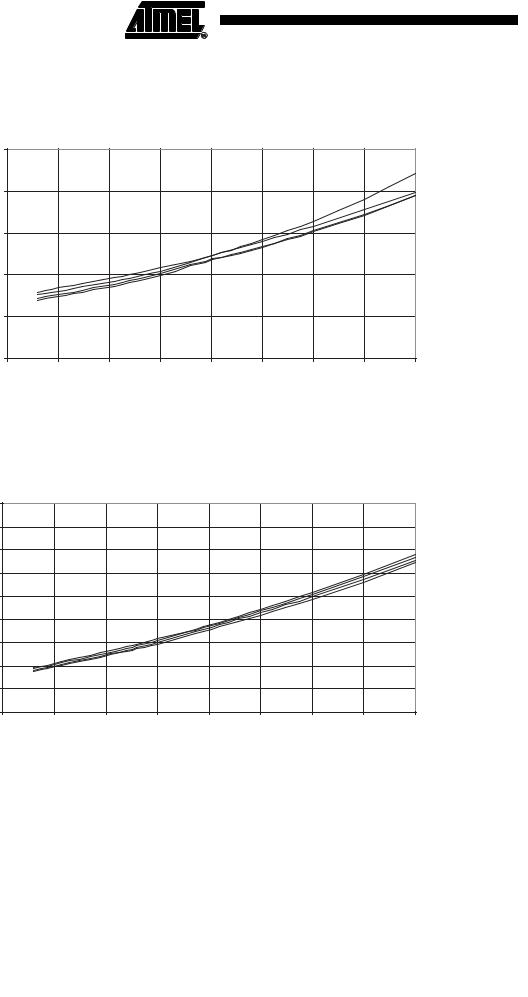
Figure 24-3. Active Supply Current vs. VCC (Internal RC Oscillator, 128 kHz)
ACTIVE SUPPLY CURRENT vs . VCC
INTERNAL RC OSCILLATOR, 128 KHz
0.25 |
|
|
|
|
|
|
|
|
|
|
|
|
|
|
|
|
125 ˚C |
|
|
|
|
|
|
|
|
85 ˚C |
0.2 |
|
|
|
|
|
|
|
25 ˚C |
|
|
|
|
|
|
|
-40 ˚C |
|
|
|
|
|
|
|
|
|
|
0.15 |
|
|
|
|
|
|
|
|
(mA) |
|
|
|
|
|
|
|
|
CC |
|
|
|
|
|
|
|
|
I |
|
|
|
|
|
|
|
|
0.1 |
|
|
|
|
|
|
|
|
0.05 |
|
|
|
|
|
|
|
|
0 |
|
|
|
|
|
|
|
|
1.5 |
2 |
2.5 |
3 |
3.5 |
4 |
4.5 |
5 |
5.5 |
|
|
|
|
VCC (V) |
|
|
|
|
Figure 24-4. Active Supply Current vs. VCC (Internal RC Oscillator, 1 MHz)
ACTIVE SUPPLY CURRENT vs . VCC
INTERNAL RC OSCILLATOR, 1 MHz
|
1.8 |
|
|
|
|
|
|
|
|
|
1.6 |
|
|
|
|
|
|
|
|
|
1.4 |
|
|
|
|
|
|
|
125 ˚C |
|
|
|
|
|
|
|
|
85 ˚C |
|
|
1.2 |
|
|
|
|
|
|
|
25 ˚C |
(mA) |
|
|
|
|
|
|
|
-40 ˚C |
|
1 |
|
|
|
|
|
|
|
|
|
CC |
|
|
|
|
|
|
|
|
|
I |
0.8 |
|
|
|
|
|
|
|
|
|
|
|
|
|
|
|
|
|
|
|
0.6 |
|
|
|
|
|
|
|
|
|
0.4 |
|
|
|
|
|
|
|
|
|
0.2 |
|
|
|
|
|
|
|
|
|
0 |
|
|
|
|
|
|
|
|
|
1.5 |
2 |
2.5 |
3 |
3.5 |
4 |
4.5 |
5 |
5.5 |
|
|
|
|
|
VCC (V) |
|
|
|
|
162 ATtiny25/45/85 Auto
7598C–AVR–09/06