
- •Features
- •1. Pin Configurations
- •2. Overview
- •2.1 Block Diagram
- •2.2 Automotive Quality Grade
- •2.3 Pin Descriptions
- •2.3.3 Port B (PB5..PB0)
- •2.3.4 RESET
- •3. About Code Examples
- •4. AVR CPU Core
- •4.1 Introduction
- •4.2 Architectural Overview
- •4.4 Status Register
- •4.5 General Purpose Register File
- •4.6 Stack Pointer
- •4.7 Instruction Execution Timing
- •4.8 Reset and Interrupt Handling
- •4.8.1 Interrupt Response Time
- •5. AVR ATtiny25/45/85 Memories
- •5.2 SRAM Data Memory
- •5.2.1 Data Memory Access Times
- •5.3 EEPROM Data Memory
- •5.3.1 EEPROM Read/Write Access
- •5.3.6 Atomic Byte Programming
- •5.3.7 Split Byte Programming
- •5.3.8 Erase
- •5.3.9 Write
- •5.3.10 Preventing EEPROM Corruption
- •5.4 I/O Memory
- •6. System Clock and Clock Options
- •6.1 Clock Systems and their Distribution
- •6.2 Clock Sources
- •6.3 Default Clock Source
- •6.4 Crystal Oscillator
- •6.6 Calibrated Internal RC Oscillator
- •6.7 External Clock
- •6.8 128 kHz Internal Oscillator
- •6.9 Clock Output Buffer
- •6.10 System Clock Prescaler
- •6.10.2 Switching Time
- •7. Power Management and Sleep Modes
- •7.1 Idle Mode
- •7.2 ADC Noise Reduction Mode
- •7.4 Power Reduction Register
- •7.5 Minimizing Power Consumption
- •7.5.1 Analog to Digital Converter
- •7.5.2 Analog Comparator
- •7.5.4 Internal Voltage Reference
- •7.5.5 Watchdog Timer
- •7.5.6 Port Pins
- •8. System Control and Reset
- •8.0.1 Resetting the AVR
- •8.0.2 Reset Sources
- •8.0.3 Power-on Reset
- •8.0.4 External Reset
- •8.0.6 Watchdog Reset
- •8.1 Internal Voltage Reference
- •8.2 Watchdog Timer
- •8.3 Timed Sequences for Changing the Configuration of the Watchdog Timer
- •8.3.1 Safety Level 1
- •8.3.2 Safety Level 2
- •9. Interrupts
- •9.1 Interrupt Vectors in ATtiny25/45/85
- •10. I/O Ports
- •10.1 Introduction
- •10.2 Ports as General Digital I/O
- •10.2.1 Configuring the Pin
- •10.2.2 Toggling the Pin
- •10.2.3 Switching Between Input and Output
- •10.2.4 Reading the Pin Value
- •10.2.5 Digital Input Enable and Sleep Modes
- •10.2.6 Unconnected Pins
- •10.3 Alternate Port Functions
- •10.3.2 Alternate Functions of Port B
- •11. External Interrupts
- •12. 8-bit Timer/Counter0 with PWM
- •12.1 Overview
- •12.1.1 Registers
- •12.1.2 Definitions
- •12.2 Timer/Counter Clock Sources
- •12.3 Counter Unit
- •12.4 Output Compare Unit
- •12.4.1 Force Output Compare
- •12.4.2 Compare Match Blocking by TCNT0 Write
- •12.4.3 Using the Output Compare Unit
- •12.5 Compare Match Output Unit
- •12.5.1 Compare Output Mode and Waveform Generation
- •12.6 Modes of Operation
- •12.6.1 Normal Mode
- •12.6.2 Clear Timer on Compare Match (CTC) Mode
- •12.6.3 Fast PWM Mode
- •12.6.4 Phase Correct PWM Mode
- •12.7 Timer/Counter Timing Diagrams
- •13. Timer/Counter Prescaler
- •13.0.1 Prescaler Reset
- •13.0.2 External Clock Source
- •14. 8-bit Timer/Counter1
- •14.1 Timer/Counter1
- •14.1.1 Timer/Counter1 Control Register - TCCR1
- •14.1.2 General Timer/Counter1 Control Register - GTCCR
- •14.1.3 Timer/Counter1 - TCNT1
- •14.1.4 Timer/Counter1 Output Compare RegisterA - OCR1A
- •14.1.5 Timer/Counter1 Output Compare RegisterB - OCR1B
- •14.1.6 Timer/Counter1 Output Compare RegisterC - OCR1C
- •14.1.7 Timer/Counter Interrupt Mask Register - TIMSK
- •14.1.8 Timer/Counter Interrupt Flag Register - TIFR
- •14.1.9 PLL Control and Status Register - PLLCSR
- •14.1.10 Timer/Counter1 Initialization for Asynchronous Mode
- •14.1.11 Timer/Counter1 in PWM Mode
- •15. 8-bit Timer/Counter1 in ATtiny15 Mode
- •15.1 Timer/Counter1 Prescaler
- •15.2 Timer/Counter1
- •15.2.2 Timer/Counter1 Control Register - TCCR1
- •15.2.3 General Timer/Counter1 Control Register - GTCCR
- •15.2.4 Timer/Counter1 - TCNT1
- •15.2.5 Timer/Counter1 Output Compare RegisterA - OCR1A
- •15.2.6 Timer/Counter1 Output Compare Register C - OCR1C
- •15.2.7 Timer/Counter Interrupt Flag Register - TIFR
- •15.2.8 PLL Control and Status Register - PLLCSR
- •15.2.9 Timer/Counter1 in PWM Mode
- •16. Dead Time Generator
- •16.0.1 Timer/Counter1 Dead Time Prescaler register 1 - DTPS1
- •16.0.2 Timer/Counter1 Dead Time A - DT1A
- •16.0.3 Timer/Counter1 Dead Time B - DT1B
- •17.1 Overview
- •17.2 Functional Descriptions
- •17.2.2 SPI Master Operation Example
- •17.2.3 SPI Slave Operation Example
- •17.2.5 Start Condition Detector
- •17.3 Alternative USI Usage
- •17.3.4 Edge Triggered External Interrupt
- •17.3.5 Software Interrupt
- •17.4 USI Register Descriptions
- •18. Analog Comparator
- •18.1 Analog Comparator Multiplexed Input
- •19. Analog to Digital Converter
- •19.1 Features
- •19.2 Operation
- •19.3 Starting a Conversion
- •19.4 Prescaling and Conversion Timing
- •19.5 Changing Channel or Reference Selection
- •19.5.1 ADC Input Channels
- •19.5.2 ADC Voltage Reference
- •19.6 ADC Noise Canceler
- •19.6.1 Analog Input Circuitry
- •19.6.2 Analog Noise Canceling Techniques
- •19.6.3 ADC Accuracy Definitions
- •19.7 ADC Conversion Result
- •19.7.1 Single Ended Conversion
- •19.7.2 Unipolar Differential Conversion
- •19.7.3 Bipolar Differential Conversion
- •19.7.4 Temperature Measurement (Preliminary description)
- •19.7.7.1 ADLAR = 0
- •19.7.7.2 ADLAR = 1
- •20. debugWIRE On-chip Debug System
- •20.1 Features
- •20.2 Overview
- •20.3 Physical Interface
- •20.4 Software Break Points
- •20.5 Limitations of debugWIRE
- •20.6 debugWIRE Related Register in I/O Memory
- •21. Self-Programming the Flash
- •21.0.1 Performing Page Erase by SPM
- •21.0.2 Filling the Temporary Buffer (Page Loading)
- •21.0.3 Performing a Page Write
- •21.1.2 EEPROM Write Prevents Writing to SPMCSR
- •21.1.3 Reading the Fuse and Lock Bits from Software
- •21.1.4 Preventing Flash Corruption
- •21.1.5 Programming Time for Flash when Using SPM
- •22. Memory Programming
- •22.1 Program And Data Memory Lock Bits
- •22.2 Fuse Bytes
- •22.2.1 Latching of Fuses
- •22.3 Signature Bytes
- •22.3.1 ATtiny25 Signature Bytes
- •22.3.2 ATtiny45 Signature Bytes
- •22.3.3 ATtiny85 Signature Bytes
- •22.4 Calibration Byte
- •22.5 Page Size
- •22.6 Serial Downloading
- •22.6.1 Serial Programming Algorithm
- •22.6.2 Serial Programming Characteristics
- •22.7 High-voltage Serial Programming
- •22.8.2 Considerations for Efficient Programming
- •22.8.3 Chip Erase
- •22.8.4 Programming the Flash
- •22.8.5 Programming the EEPROM
- •22.8.6 Reading the Flash
- •22.8.7 Reading the EEPROM
- •22.8.8 Programming and Reading the Fuse and Lock Bits
- •22.8.9 Reading the Signature Bytes and Calibration Byte
- •23. Electrical Characteristics
- •23.1 Absolute Maximum Ratings*
- •23.2 External Clock Drive Waveforms
- •23.3 External Clock Drive
- •23.5 Calibrated RC Oscillator Accuracy
- •24. Typical Characteristics
- •24.1 Active Supply Current
- •24.2 Idle Supply Current
- •24.2.1 Using the Power Reduction Register
- •24.2.1.1 Example 1
- •24.5 Pin Driver Strength
- •24.6 Pin Thresholds and Hysteresis
- •24.7 BOD Thresholds and Analog Comparator Offset
- •24.8 Internal Oscillator Speed
- •24.9 Current Consumption of Peripheral Units
- •24.10 Current Consumption in Reset and Reset Pulse width
- •24.11 Analog to Digital Converter
- •25. Register Summary
- •26. Instruction Set Summary
- •27. Ordering Information
- •28. Packaging Information
- •29. Document Revision History
- •30. Errata
- •30.1 ATtiny25/45/85 Rev. A

ATtiny25/45/85 Auto
Table 22-10. Serial Programming Instruction Set
|
|
|
|
Instruction Format |
|
|
||
|
|
|
|
|
|
|||
Instruction |
Byte 1 |
Byte 2 |
Byte 3 |
Byte4 |
Operation |
|||
|
|
|
|
|
|
|
|
|
|
|
|
0101 |
0000 |
xxxx |
oooo |
Read Fuse bits. “0” = |
|
Read Fuse bits |
0000 |
0000 |
xxxx |
oooo |
programmed, “1” = |
|||
|
|
|
|
unprogrammed. See Table |
||||
|
|
|
|
|
|
|
||
|
|
|
|
|
|
|
22-5 on page 141 for details. |
|
|
|
|
|
|
|
|
|
|
|
|
|
0101 |
0000 |
xxxx |
oooo |
Read Fuse High bits. “0” = |
|
Read Fuse High bits |
1000 |
1000 |
xxxx |
oooo |
pro-grammed, “1” = |
|||
|
|
|
|
unprogrammed. See Table |
||||
|
|
|
|
|
|
|
||
|
|
|
|
|
|
|
22-4 on page 141 for details. |
|
|
|
|
|
|
|
|
|
|
|
|
|
0101 |
0000 |
xxxx |
oooo |
Read Extended Fuse bits. “0” |
|
Read Extended Fuse |
0000 |
1000 |
xxxx |
oooo |
= pro-grammed, “1” = |
|||
Bits |
|
|
|
|
unprogrammed. See Table |
|||
|
|
|
|
|
|
|
22-3 on page 140 for details. |
|
|
|
|
|
|
|
|
|
|
Read Calibration Byte |
0011 |
000x |
0000 |
oooo |
Read Calibration Byte |
|||
1000 |
xxxx |
0000 |
oooo |
|||||
|
|
|
|
|||||
|
|
|
|
|
|
|
|
|
|
|
|
1111 |
0000 |
xxxx |
xxxx |
If o = “1”, a programming |
|
|
|
|
0000 |
0000 |
xxxx |
xxxo |
operation is still busy. Wait |
|
Poll RDY/BSY |
|
|
|
|
|
until this bit returns to “0” |
||
|
|
|
|
|
|
|
before applying another |
|
|
|
|
|
|
|
|
command. |
|
|
|
|
|
|
|
|
|
Note: a = address high bits, b = address low bits, H = 0 - Low byte, 1 - High Byte, o = data out, i = data in, x = don’t care
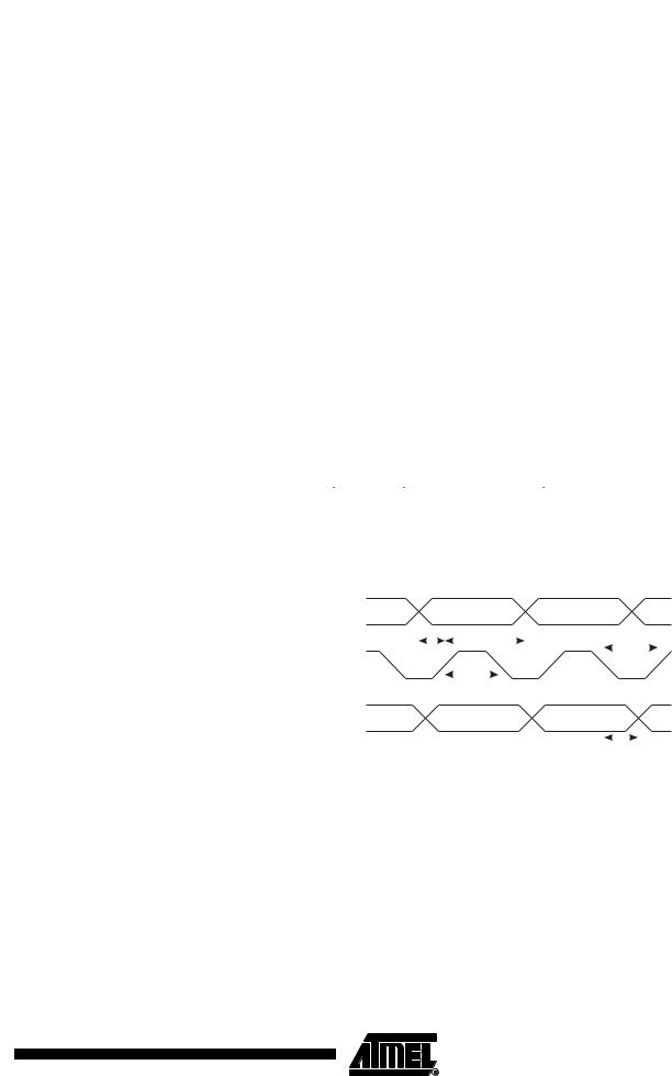
22.6.2Serial Programming Characteristics
Figure 22-3. Serial Programming Timing
|
MOSI |
|
|
|
|
|
|
|
|
|
|
|
|
|
|
|
|
|
|
|
|
tOVSH |
|
|
|
|
|
|
|
|
|
tSHOX |
|
tSLSH |
|
|
|
||||
|
|
|
|
|
|
|
|
|
|
|
|
|
|
|||||||
|
SCK |
|
|
|
|
|
|
|
|
|
|
|
|
|
|
|
|
|
|
|
|
|
|
|
|
|
|
|
|
|
|
|
|
|
|
|
|
|
|
|
|
|
|
|
|
|
|
tSHSL |
|
|
|
|
|
|
|
|
|
|
|
|
||
|
|
|
|
|
|
|
|
|
|
|
|
|
|
|
|
|
|
|
||
|
|
|
|
|
|
|
|
|
|
|
|
|
|
|
||||||
|
MISO |
|
|
|
|
|
|
|
|
|
|
|
|
|||||||
|
|
|
|
|
|
|
|
|
|
|
|
|
|
|
|
tSLIV |
|
|
||
|
|
|
|
|
|
|
|
|
|
|
|
|
|
|
|
|
|
|||
|
|
|
|
|
|
|
|
|
|
|
|
|
|
|
|
|
|
|||
Table 22-11. Serial Programming Characteristics, TA = -40°C to 125°C, VCC = 2.7 - 5.5V |
||||||||||||||||||||
|
(Unless Otherwise Noted) |
|
|
|
|
|
|
|
|
|
|
|
|
|||||||
|
|
|
|
|
|
|
|
|
|
|
|
|
|
|
|
|
|
|
|
|
Symbol |
Parameter |
|
|
|
|
Min |
|
|
Typ |
Max |
Units |
|||||||||
|
|
|
|
|
|
|
|
|
|
|
|
|
|
|
|
|
|
|
|
|
1/tCLCL |
Oscillator Frequency (ATtiny25/45/85V) |
|
|
|
0 |
|
|
|
|
4 |
MHz |
|||||||||
tCLCL |
Oscillator Period (ATtiny25/45/85V) |
|
|
|
250 |
|
|
|
|
|
ns |
|||||||||
1/tCLCL |
Oscillator Frequency (ATtiny25/45/85L, VCC = 2.7 - |
0 |
|
|
|
|
10 |
MHz |
||||||||||||
5.5V) |
|
|
|
|
|
|
|
|||||||||||||
tCLCL |
Oscillator Period (ATtiny25/45/85L, VCC = 2.7 - |
100 |
|
|
|
|
|
ns |
||||||||||||
5.5V) |
|
|
|
|
|
|
|
|
147
7598C–AVR–09/06