

symmetry around BOTTOM the OCn value at MAX must correspond to the result of an upcounting Compare Match.
•The timer starts counting from a value higher than the one in OCR0A, and for that reason misses the Compare Match and hence the OCn change that would have happened on the way up.
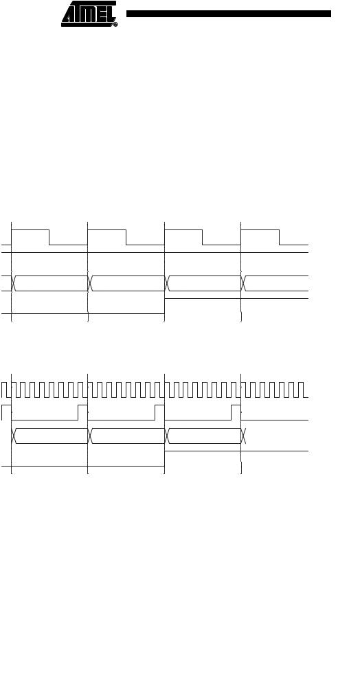
12.7Timer/Counter Timing Diagrams
The Timer/Counter is a synchronous design and the timer clock (clkT0) is therefore shown as a clock enable signal in the following figures. The figures include information on when Interrupt Flags are set. Figure 12-8 contains timing data for basic Timer/Counter operation. The figure shows the count sequence close to the MAX value in all modes other than phase correct PWM mode.
Figure 12-8. Timer/Counter Timing Diagram, no Prescaling
clkI/O
clkTn
(clkI/O/1)
TCNTn |
MAX - 1 |
|
MAX |
|
BOTTOM |
|
BOTTOM + 1 |
|
|
|
|
|
|
|
|
TOVn
Figure 12-9 shows the same timing data, but with the prescaler enabled.
Figure 12-9. Timer/Counter Timing Diagram, with Prescaler (fclk_I/O/8)
clkI/O
clkTn
(clkI/O/8)
TCNTn |
|
|
MAX - 1 |
|
MAX |
|
BOTTOM |
|
|
BOTTOM + 1 |
|
|
|
|
|
|
|
|
|
|
|
TOVn
Figure 12-10 shows the setting of OCF0B in all modes and OCF0A in all modes except CTC mode and PWM mode, where OCR0A is TOP.
70 ATtiny25/45/85 Auto 
7598C–AVR–09/06
 ATtiny25/45/85 Auto
Figure 12-10. Timer/Counter Timing Diagram, Setting of OCF0x, with Prescaler (fclk_I/O/8)
clkI/O |
|
|
|
|
|
|
|
|
|
|
|
|
|
|
|
|
|
|
|
|
|
|
|
|
|
|
|
|
|
|
|
|
|
|
|
|
|
|
|
|
|
|
|
|
|
|
|
|
|
|
|
|
|
|
|
|
|
|
|
|
|
|
|
|
clkTn |
|
|
|
|
|
|
|
|
|
|
|
|
|
|
|
|
|
|
|
|
|
|
|
|
|
|
|
|
|
|
|
|
|
|
|
|
|
|
|
|
|
|
|
|
|
|
|
|
|
|
|
|
|
|
|
|
|
|
|
|
|
|
|
|
|
|
|
|
|
|
|
|
|
|
|
|
|
|
|
|
|
|
|
|
|
|
|
|
|
|
|
|
|
|
|
|
|
|
|
|
|
|
|
|
|
|
|
|
|
|
|
|
|
|
|
|
|
|
|
|
|
|
|
|
|
|
|
|
|
|
|
|
|
|
|
|
|
|
|
|
|
|
|
|
|
|
|
|
|
|
|
|
|
|
|
|
|
|
|
|
|
|
|
|
|
|
|
|
|
|
|
|
|
|
|
|
|
|
|
|
|
|
|
|
|
|
|
|
|
|
|
|
|
|
(clkI/O/8) |
|
|
|
|
|
|
|
|
|
|
|
|
|
|
|
|
|
|
|
|
|
|
|
|
|
|
|
|
|
|
|
|
|
|
|
|
|
|
|
|
|
|
|
|
|
|
|
|
|
|
|
|
|
|
|
|
|
|
|
|
|
|
|
|
TCNTn |
|
|
|
|
|
|
|
|
|
|
|
|
|
|
|
|
|
|
|
|
|
|
|
|
|
|
|
|
|
|
|
|
|
|
|
|||||||||||||||||||||||||||||
|
|
|
|
|
|
|
|
OCRnx - 1 |
|
|
|
|
|
|
|
|
|
|
OCRnx |
|
|
|
|
|
|
|
|
OCRnx + 1 |
|
|
|
|
|
|
|
|
OCRnx + 2 |
|
|
|||||||||||||||||||||||||
OCRnx |
|
|
|
|
|
|
|
|
|
|
|
|
|
|
|
|
|
|
|
|
|
|
|
|
|
|
|
|
|
|
|
|
|
|
|
|
|
|
|
|
|
|
|
|
|
|
|
|
|
|
|
|
|
|
|
|
|
|||||||
|
|
|
|
|
|
|
|
|
|
|
|
|
|
|
|
|
|
|
|
|
|
|
|
|
|
|
|
|
|
|
|
|
|
|
|
|
|
|
|
|
|
|
|
|
|
|
|
|
|
|
|
|
|
|
|
|
|
|
|
|
|
|
|
|
|
|
|
|
|
|
|
|
|
|
|
|
|
|
|
|
|
|
|
|
|
|
|
|
|
|
|
|
|
OCRnx Value |
|
|
|
|
|
|
|
|
|
|
|
|
|
|
|
|
|
|
|
|
|
|
|
|
|
|
|||||||||
OCFnx |
|
|
|
|
|
|
|
|
|
|
|
|
|
|
|
|
|
|
|
|
|
|
|
|
|
|
|
|
|
|
|
|
|
|
|
|
|
|
|
|
|
|
|
|
|
|
|
|
|
|
|
|
|
|
|
|
|
|
|
|
|
|
|
|
|
|
|
|
|
|
|
|
|
|
|
|
|
|
|
|
|
|
|
|
|
|
|
|
|
|
|
|
|
|
|
|
|
|
|
|
|
|
|
|
|
|
|
|
|
|
|
|
|
|
|
|
|
|
|
|
|
|
|
|
|
|
|
|
|
|
|
|
|
|
|
|
|
|
|
|
|
|
|
|
|
|
|
|
|
|
|
|
|
|
|
|
|
|
|
|
|
|
|
|
|
|
|
|
|
|
|
|
|
|
|
|
|
|
|
|
|
|
|
|
|
|
|
|
|
|
|
|
|
|
|
|
|
|
|
|
|
|
|
|
|
|
|
|
|
|
|
|
|
|
|
|
|
|
|
|
|
|
|
|
|
|
|
|
|
|
|
|
|
|
|
|
|
|
|
|
|
|
|
|
|
|
|
|
|
|
|
|
|
|
|
|
|
|
|
Figure 12-11 shows the setting of OCF0A and the clearing of TCNT0 in CTC mode and fast PWM mode where OCR0A is TOP.
Figure 12-11. Timer/Counter Timing Diagram, Clear Timer on Compare Match mode, with Prescaler (fclk_I/O/8)
clkI/O |
|
|
|
|
|
clkTn |
|
|
|
|
|
(clkI/O/8) |
|
|
|
|
|
TCNTn |
TOP - 1 |
TOP |
BOTTOM |
BOTTOM + 1 |
|
(CTC) |
|||||
|
|
|
|
||
OCRnx |
|
|
TOP |
|
|
OCFnx |
|
|
|
|
12.88-bit Timer/Counter Register Description
12.8.1Timer/Counter Control Register A – TCCR0A
Bit |
7 |
6 |
5 |
4 |
3 |
2 |
1 |
0 |
|
|
COM0A1 |
COM0A0 |
COM0B1 |
COM0B0 |
– |
– |
WGM01 |
WGM00 |
TCCR0A |
|
|
|
|
|
|
|
|
|
|
Read/Write |
R/W |
R/W |
R/W |
R/W |
R |
R |
R/W |
R/W |
|
Initial Value |
0 |
0 |
0 |
0 |
0 |
0 |
0 |
0 |
|
• Bits 7:6 – COM01A:0: Compare Match Output A Mode
These bits control the Output Compare pin (OC0A) behavior. If one or both of the COM0A1:0 bits are set, the OC0A output overrides the normal port functionality of the I/O pin it is connected to. However, note that the Data Direction Register (DDR) bit corresponding to the OC0A pin must be set in order to enable the output driver.
71
7598C–AVR–09/06

When OC0A is connected to the pin, the function of the COM0A1:0 bits depends on the WGM02:0 bit setting. Table 12-1 shows the COM0A1:0 bit functionality when the WGM02:0 bits are set to a normal or CTC mode (non-PWM).
Table 12-1. |
Compare Output Mode, non-PWM Mode |
|
COM01 |
COM00 |
Description |
|
|
|
0 |
0 |
Normal port operation, OC0A disconnected. |
|
|
|
0 |
1 |
Toggle OC0A on Compare Match |
|
|
|
1 |
0 |
Clear OC0A on Compare Match |
|
|
|
1 |
1 |
Set OC0A on Compare Match |
|
|
|
Table 12-2 shows the COM0A1:0 bit functionality when the WGM01:0 bits are set to fast PWM mode.
Table 12-2. |
Compare Output Mode, Fast PWM Mode(1) |
||
COM01 |
COM00 |
Description |
|
|
|
|
|
0 |
0 |
Normal port operation, OC0A disconnected. |
|
|
|
|
|
0 |
1 |
WGM02 = 0: Normal Port Operation, OC0A Disconnected. |
|
WGM02 = 1: Toggle OC0A on Compare Match. |
|||
|
|
||
|
|
|
|
1 |
0 |
Clear OC0A on Compare Match, set OC0A at TOP |
|
|
|
|
|
1 |
1 |
Set OC0A on Compare Match, clear OC0A at TOP |
|
|
|
|
|
Note: 1. A special case occurs when OCR0A equals TOP and COM0A1 is set. In this case, the Compare Match is ignored, but the set or clear is done at TOP. See “Fast PWM Mode” on page 67 for more details.
Table 12-3 shows the COM0A1:0 bit functionality when the WGM02:0 bits are set to phase correct PWM mode.
Table 12-3. Compare Output Mode, Phase Correct PWM Mode(1)
COM0A1 |
|
COM0A0 |
Description |
|
|
|
|
0 |
|
0 |
Normal port operation, OC0A disconnected. |
|
|
|
|
0 |
|
1 |
WGM02 = 0: Normal Port Operation, OC0A Disconnected. |
|
WGM02 = 1: Toggle OC0A on Compare Match. |
||
|
|
|
|
|
|
|
|
1 |
|
0 |
Clear OC0A on Compare Match when up-counting. Set OC0A on |
|
Compare Match when down-counting. |
||
|
|
|
|
|
|
|
|
1 |
|
1 |
Set OC0A on Compare Match when up-counting. Clear OC0A on |
|
Compare Match when down-counting. |
||
|
|
|
|
|
|
|
|
Note: 1. |
A special case occurs when OCR0A equals TOP and COM0A1 is set. In this case, the Com- |
||
|
pare Match is ignored, but the set or clear is done at TOP. See “Phase Correct PWM Mode” on |
||
|
page 68 for more details. |
||
• Bits 5:4 – COM0B1:0: Compare Match Output B Mode
These bits control the Output Compare pin (OC0B) behavior. If one or both of the COM0B1:0 bits are set, the OC0B output overrides the normal port functionality of the I/O pin it is connected to. However, note that the Data Direction Register (DDR) bit corresponding to the OC0B pin must be set in order to enable the output driver.
72 ATtiny25/45/85 Auto 
7598C–AVR–09/06

ATtiny25/45/85 Auto
When OC0B is connected to the pin, the function of the COM0B1:0 bits depends on the WGM02:0 bit setting. Table 12-1 shows the COM0A1:0 bit functionality when the WGM02:0 bits are set to a normal or CTC mode (non-PWM).
Table 12-4. |
Compare Output Mode, non-PWM Mode |
|
COM01 |
COM00 |
Description |
|
|
|
0 |
0 |
Normal port operation, OC0B disconnected. |
|
|
|
0 |
1 |
Toggle OC0B on Compare Match |
|
|
|
1 |
0 |
Clear OC0B on Compare Match |
|
|
|
1 |
1 |
Set OC0B on Compare Match |
|
|
|
Table 12-2 shows the COM0B1:0 bit functionality when the WGM02:0 bits are set to fast PWM mode.
Table 12-5. |
Compare Output Mode, Fast PWM Mode(1) |
|
COM01 |
COM00 |
Description |
|
|
|
0 |
0 |
Normal port operation, OC0B disconnected. |
|
|
|
0 |
1 |
Reserved |
|
|
|
1 |
0 |
Clear OC0B on Compare Match, set OC0B at TOP |
|
|
|
1 |
1 |
Set OC0B on Compare Match, clear OC0B at TOP |
|
|
|
Note: 1. A special case occurs when OCR0B equals TOP and COM0B1 is set. In this case, the Compare Match is ignored, but the set or clear is done at TOP. See “Fast PWM Mode” on page 67 for more details.
Table 12-3 shows the COM0B1:0 bit functionality when the WGM02:0 bits are set to phase correct PWM mode.
Table 12-6. Compare Output Mode, Phase Correct PWM Mode(1)
COM0A1 |
|
COM0A0 |
Description |
|
|
|
|
0 |
|
0 |
Normal port operation, OC0B disconnected. |
|
|
|
|
0 |
|
1 |
Reserved |
|
|
|
|
1 |
|
0 |
Clear OC0B on Compare Match when up-counting. Set OC0B on |
|
Compare Match when down-counting. |
||
|
|
|
|
|
|
|
|
1 |
|
1 |
Set OC0B on Compare Match when up-counting. Clear OC0B on |
|
Compare Match when down-counting. |
||
|
|
|
|
|
|
|
|
Note: 1. |
A special case occurs when OCR0B equals TOP and COM0B1 is set. In this case, the Com- |
||
|
pare Match is ignored, but the set or clear is done at TOP. See “Phase Correct PWM Mode” on |
||
|
page 68 for more details. |
||
• Bits 3, 2 – Res: Reserved Bits
These bits are reserved bits in the ATtiny25/45/85 and will always read as zero.
• Bits 1:0 – WGM01:0: Waveform Generation Mode
Combined with the WGM02 bit found in the TCCR0B Register, these bits control the counting sequence of the counter, the source for maximum (TOP) counter value, and what type of waveform generation to be used, see Table 12-7. Modes of operation supported by the Timer/Counter
73
7598C–AVR–09/06

unit are: Normal mode (counter), Clear Timer on Compare Match (CTC) mode, and two types of Pulse Width Modulation (PWM) modes (see “Modes of Operation” on page 65).
Table 12-7. Waveform Generation Mode Bit Description
|
|
|
|
|
Timer/Counter |
|
|
|
|
|
|
|
|
Mode of |
|
Update of |
TOV Flag |
Mode |
|
WGM2 |
WGM1 |
WGM0 |
Operation |
TOP |
OCRx at |
Set on(1)(2) |
0 |
|
0 |
0 |
0 |
Normal |
0xFF |
Immediate |
MAX |
|
|
|
|
|
|
|
|
|
1 |
|
0 |
0 |
1 |
PWM, Phase |
0xFF |
TOP |
BOTTOM |
|
Correct |
|||||||
|
|
|
|
|
|
|
|
|
|
|
|
|
|
|
|
|
|
2 |
|
0 |
1 |
0 |
CTC |
OCRA |
Immediate |
MAX |
|
|
|
|
|
|
|
|
|
3 |
|
0 |
1 |
1 |
Fast PWM |
0xFF |
TOP |
MAX |
|
|
|
|
|
|
|
|
|
4 |
|
1 |
0 |
0 |
Reserved |
– |
– |
– |
|
|
|
|
|
|
|
|
|
5 |
|
1 |
0 |
1 |
PWM, Phase |
OCRA |
TOP |
BOTTOM |
|
Correct |
|||||||
|
|
|
|
|
|
|
|
|
|
|
|
|
|
|
|
|
|
6 |
|
1 |
1 |
0 |
Reserved |
– |
– |
– |
|
|
|
|
|
|
|
|
|
7 |
|
1 |
1 |
1 |
Fast PWM |
OCRA |
TOP |
TOP |
|
|
|
|
|
|
|
|
|
Notes: |
1. MAX |
= 0xFF |
|
|
|
|
|
|
2.BOTTOM = 0x00
12.8.2Timer/Counter Control Register B – TCCR0B
Bit |
7 |
6 |
5 |
4 |
3 |
2 |
1 |
0 |
|
|
FOC0A |
FOC0B |
– |
– |
WGM02 |
CS02 |
CS01 |
CS00 |
TCCR0B |
|
|
|
|
|
|
|
|
|
|
Read/Write |
W |
W |
R |
R |
R |
R |
R/W |
R/W |
|
Initial Value |
0 |
0 |
0 |
0 |
0 |
0 |
0 |
0 |
|
• Bit 7 – FOC0A: Force Output Compare A
The FOC0A bit is only active when the WGM bits specify a non-PWM mode.
However, for ensuring compatibility with future devices, this bit must be set to zero when TCCR0B is written when operating in PWM mode. When writing a logical one to the FOC0A bit, an immediate Compare Match is forced on the Waveform Generation unit. The OC0A output is changed according to its COM0A1:0 bits setting. Note that the FOC0A bit is implemented as a strobe. Therefore it is the value present in the COM0A1:0 bits that determines the effect of the forced compare.
A FOC0A strobe will not generate any interrupt, nor will it clear the timer in CTC mode using OCR0A as TOP.
The FOC0A bit is always read as zero.
• Bit 6 – FOC0B: Force Output Compare B
The FOC0B bit is only active when the WGM bits specify a non-PWM mode.
However, for ensuring compatibility with future devices, this bit must be set to zero when TCCR0B is written when operating in PWM mode. When writing a logical one to the FOC0B bit, an immediate Compare Match is forced on the Waveform Generation unit. The OC0B output is changed according to its COM0B1:0 bits setting. Note that the FOC0B bit is implemented as a
74 ATtiny25/45/85 Auto 
7598C–AVR–09/06

 ATtiny25/45/85 Auto
strobe. Therefore it is the value present in the COM0B1:0 bits that determines the effect of the forced compare.
A FOC0B strobe will not generate any interrupt, nor will it clear the timer in CTC mode using OCR0B as TOP.
The FOC0B bit is always read as zero.
• Bits 5:4 – Res: Reserved Bits
These bits are reserved bits in the ATtiny25/45/85 and will always read as zero.
• Bit 3 – WGM02: Waveform Generation Mode
See the description in the “Timer/Counter Control Register A – TCCR0A” on page 71.
• Bits 2:0 – CS02:0: Clock Select
The three Clock Select bits select the clock source to be used by the Timer/Counter.
Table 12-8. Clock Select Bit Description
CS02 |
CS01 |
CS00 |
Description |
|
|
|
|
0 |
0 |
0 |
No clock source (Timer/Counter stopped) |
|
|
|
|
0 |
0 |
1 |
clkI/O/(No prescaling) |
0 |
1 |
0 |
clkI/O/8 (From prescaler) |
0 |
1 |
1 |
clkI/O/64 (From prescaler) |
1 |
0 |
0 |
clkI/O/256 (From prescaler) |
1 |
0 |
1 |
clkI/O/1024 (From prescaler) |
|
|
|
|
1 |
1 |
0 |
External clock source on T0 pin. Clock on falling edge. |
|
|
|
|
1 |
1 |
1 |
External clock source on T0 pin. Clock on rising edge. |
|
|
|
|
If external pin modes are used for the Timer/Counter0, transitions on the T0 pin will clock the counter even if the pin is configured as an output. This feature allows software control of the counting.
12.8.3Timer/Counter Register – TCNT0
Bit |
7 |
6 |
5 |
4 |
3 |
2 |
1 |
0 |
|
|
|
|
|
TCNT0[7:0] |
|
|
|
TCNT0 |
|
|
|
|
|
|
|
|
|
|
|
Read/Write |
R/W |
R/W |
R/W |
R/W |
R/W |
R/W |
R/W |
R/W |
|
Initial Value |
0 |
0 |
0 |
0 |
0 |
0 |
0 |
0 |
|
The Timer/Counter Register gives direct access, both for read and write operations, to the Timer/Counter unit 8-bit counter. Writing to the TCNT0 Register blocks (removes) the Compare Match on the following timer clock. Modifying the counter (TCNT0) while the counter is running, introduces a risk of missing a Compare Match between TCNT0 and the OCR0x Registers.
12.8.4Output Compare Register A – OCR0A
Bit |
7 |
6 |
5 |
4 |
3 |
2 |
1 |
0 |
|
|
|
|
|
OCR0A[7:0] |
|
|
|
OCR0A |
|
|
|
|
|
|
|
|
|
|
|
Read/Write |
R/W |
R/W |
R/W |
R/W |
R/W |
R/W |
R/W |
R/W |
|
Initial Value |
0 |
0 |
0 |
0 |
0 |
0 |
0 |
0 |
|
75
7598C–AVR–09/06

The Output Compare Register A contains an 8-bit value that is continuously compared with the counter value (TCNT0). A match can be used to generate an Output Compare interrupt, or to generate a waveform output on the OC0A pin.
12.8.5Output Compare Register B – OCR0B
Bit |
7 |
6 |
5 |
4 |
3 |
2 |
1 |
0 |
|
|
|
|
|
OCR0B[7:0] |
|
|
|
OCR0B |
|
|
|
|
|
|
|
|
|
|
|
Read/Write |
R/W |
R/W |
R/W |
R/W |
R/W |
R/W |
R/W |
R/W |
|
Initial Value |
0 |
0 |
0 |
0 |
0 |
0 |
0 |
0 |
|
The Output Compare Register B contains an 8-bit value that is continuously compared with the counter value (TCNT0). A match can be used to generate an Output Compare interrupt, or to generate a waveform output on the OC0B pin.
12.8.6Timer/Counter Interrupt Mask Register – TIMSK
Bit |
7 |
6 |
5 |
4 |
3 |
2 |
1 |
0 |
|
|
– |
OCIE1A |
OCIE1B |
OCIE0A |
OCIE0B |
TOIE1 |
TOIE0 |
– |
TIMSK |
Read/Write |
R |
R |
R |
R |
R/W |
R/W |
R/W |
R |
|
Initial Value |
0 |
0 |
0 |
0 |
0 |
0 |
0 |
0 |
|
• Bits 7..4, 0 – Res: Reserved Bits
These bits are reserved bits in the ATtiny25/45/85 and will always read as zero.
• Bit 3 – OCIE0B: Timer/Counter Output Compare Match B Interrupt Enable
When the OCIE0B bit is written to one, and the I-bit in the Status Register is set, the Timer/Counter Compare Match B interrupt is enabled. The corresponding interrupt is executed if a Compare Match in Timer/Counter occurs, i.e., when the OCF0B bit is set in the Timer/Counter Interrupt Flag Register – TIFR0.
• Bit 2 – OCIE0A: Timer/Counter0 Output Compare Match A Interrupt Enable
When the OCIE0A bit is written to one, and the I-bit in the Status Register is set, the Timer/Counter0 Compare Match A interrupt is enabled. The corresponding interrupt is executed if a Compare Match in Timer/Counter0 occurs, i.e., when the OCF0A bit is set in the Timer/Counter 0 Interrupt Flag Register – TIFR0.
• Bit 1 – TOIE0: Timer/Counter0 Overflow Interrupt Enable
When the TOIE0 bit is written to one, and the I-bit in the Status Register is set, the Timer/Counter0 Overflow interrupt is enabled. The corresponding interrupt is executed if an overflow in Timer/Counter0 occurs, i.e., when the TOV0 bit is set in the Timer/Counter 0 Interrupt Flag Register – TIFR0.
12.8.7Timer/Counter 0 Interrupt Flag Register – TIFR
Bit |
7 |
6 |
5 |
4 |
3 |
2 |
1 |
0 |
|
|
– |
OCF1A |
OCF1B |
OCF0A |
OCF0B |
TOV1 |
TOV0 |
– |
TIFR |
Read/Write |
R |
R |
R |
R |
R/W |
R/W |
R/W |
R |
|
Initial Value |
0 |
0 |
0 |
0 |
0 |
0 |
0 |
0 |
|
• Bits 7, 0 – Res: Reserved Bits
These bits are reserved bits in the ATtiny25/45/85 and will always read as zero.
• Bit 4– OCF0A: Output Compare Flag 0 A
76 ATtiny25/45/85 Auto
7598C–AVR–09/06