

ATtiny25/45/85 Auto
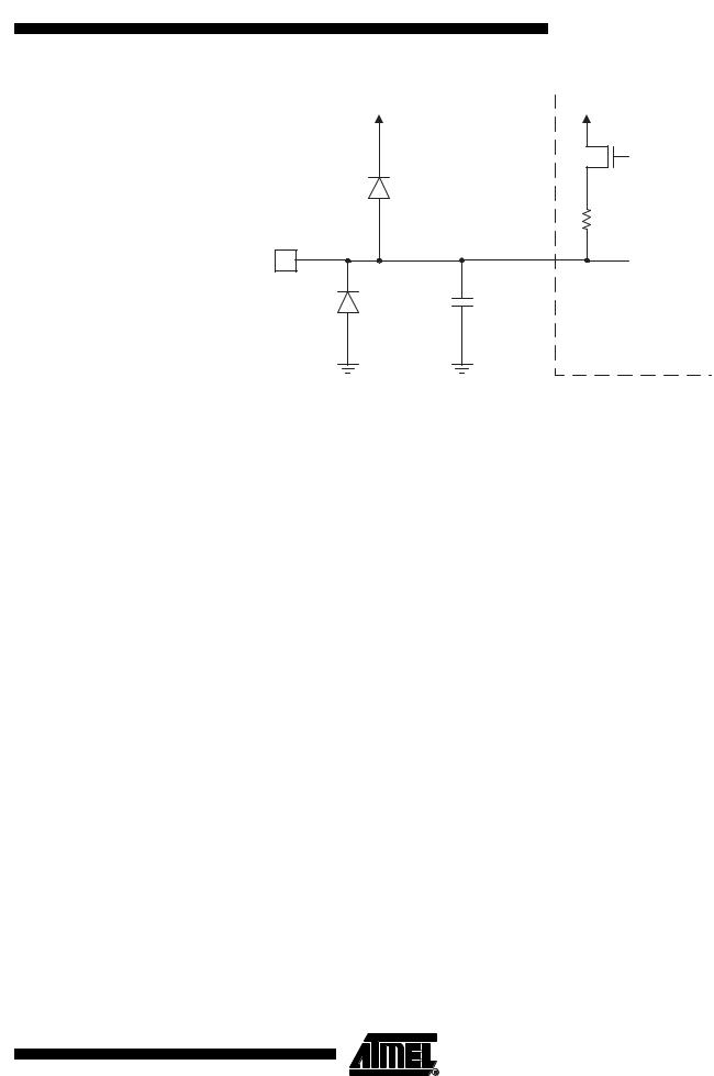
Figure 10-1. I/O Pin Equivalent Schematic
|
Rpu |
Pxn |
Logic |
Cpin |
See Figure |
|
"General Digital I/O" for |
|
Details |
All registers and bit references in this section are written in general form. A lower case “x” represents the numbering letter for the port, and a lower case “n” represents the bit number. However, when using the register or bit defines in a program, the precise form must be used. For example, PORTB3 for bit no. 3 in Port B, here documented generally as PORTxn. The physical I/O Registers and bit locations are listed in “Register Description for I/O-Ports” on page 57.
Three I/O memory address locations are allocated for each port, one each for the Data Register
– PORTx, Data Direction Register – DDRx, and the Port Input Pins – PINx. The Port Input Pins I/O location is read only, while the Data Register and the Data Direction Register are read/write. However, writing a logic one to a bit in the PINx Register, will result in a toggle in the corresponding bit in the Data Register. In addition, the Pull-up Disable – PUD bit in MCUCR disables the pull-up function for all pins in all ports when set.
Using the I/O port as General Digital I/O is described in “Ports as General Digital I/O” on page 47. Most port pins are multiplexed with alternate functions for the peripheral features on the device. How each alternate function interferes with the port pin is described in “Alternate Port Functions” on page 52. Refer to the individual module sections for a full description of the alternate functions.
Note that enabling the alternate function of some of the port pins does not affect the use of the other pins in the port as general digital I/O.
10.2Ports as General Digital I/O
The ports are bi-directional I/O ports with optional internal pull-ups. Figure 10-2 shows a functional description of one I/O-port pin, here generically called Pxn.
47
7598C–AVR–09/06
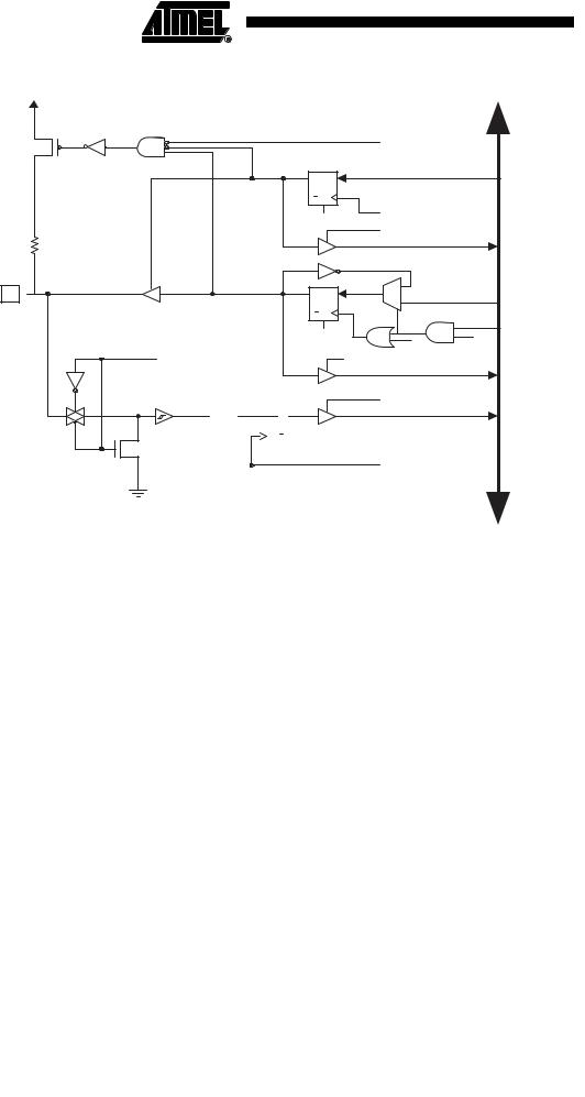
Figure 10-2. General Digital I/O(1)
Pxn 

SLEEP
SYNCHRONIZER
|
|
|
|
|
|
|
|
|
|
|
|
|
|
|
|
|
|
|
|
|
|
|
|
|
|
|
|
|
|
|
|
|
D |
Q |
|
|
|
|
|
|
|
D Q |
|
|
|||||||||
|
|
|
|
|
|
|
|
|
|
|
|
|
|
|
|
|
|
|
|
PINxn |
|
|
||||
|
|
|
|
|
|
|
|
|
|
|
|
|
|
|
|
|
|
|
|
|
|
|||||
|
|
|
|
|
|
L |
Q |
|
|
|
|
|
|
|
|
|
|
Q |
|
|
||||||
|
|
|
|
|
|
|
|
|
|
|
|
|
|
|
|
|
|
|
|
|
|
|
|
|
|
|
|
|
|
|
|
|
|
|
|
|
|
|
|
|
|
|
|
|
|
|
|
|
|
|
|
|
|
|
|
|
|
|
|
|
|
|
|
|
|
|
|
|
|
|
|
|
|
|
|
|
|
|
|
|
|
|
|
|
|
|
|
|
|
|
|
|
|
|
|
|
|
|
|
|
|
|
|
|
|
|
|
|
|
|
|
|
|
|
|
|
|
|
|
|
|
|
|
|
|
|
|
|
|
|
|
|
|
|
|
|
PUD |
|
|
Q |
D |
|
|
|
DDxn |
|
|
||
Q CLR |
|
|
|
|
RESET |
WDx |
|
||
RDx |
|
|||
|
|
|
||
Q |
D |
1 |
BUS |
|
|
DATA |
|||
PORTxn |
0 |
|||
|
||||
Q CLR |
|
|
|
|
RESET |
|
WPx |
||
|
|
WRx |
||
|
|
|
||
|
|
RRx |
|
|
|
|
RPx |
|
|
|
|
clk I/O |
|
|
PUD: |
PULLUP DISABLE |
WDx: |
WRITE DDRx |
RDx: |
READ DDRx |
||
SLEEP: |
SLEEP CONTROL |
WRx: |
WRITE PORTx |
clkI/O: |
I/O CLOCK |
RRx: |
READ PORTx REGISTER |
|
|
RPx: |
READ PORTx PIN |
|
|
WPx: |
WRITE PINx REGISTER |
Note: 1. WRx, WPx, WDx, RRx, RPx, and RDx are common to all pins within the same port. clkI/O,
SLEEP, and PUD are common to all ports.
10.2.1Configuring the Pin
Each port pin consists of three register bits: DDxn, PORTxn, and PINxn. As shown in “Register Description for I/O-Ports” on page 57, the DDxn bits are accessed at the DDRx I/O address, the PORTxn bits at the PORTx I/O address, and the PINxn bits at the PINx I/O address.
The DDxn bit in the DDRx Register selects the direction of this pin. If DDxn is written logic one, Pxn is configured as an output pin. If DDxn is written logic zero, Pxn is configured as an input pin.
If PORTxn is written logic one when the pin is configured as an input pin, the pull-up resistor is activated. To switch the pull-up resistor off, PORTxn has to be written logic zero or the pin has to be configured as an output pin. The port pins are tri-stated when reset condition becomes active, even if no clocks are running.
If PORTxn is written logic one when the pin is configured as an output pin, the port pin is driven high (one). If PORTxn is written logic zero when the pin is configured as an output pin, the port pin is driven low (zero).
10.2.2Toggling the Pin
Writing a logic one to PINxn toggles the value of PORTxn, independent on the value of DDRxn. Note that the SBI instruction can be used to toggle one single bit in a port.
48 ATtiny25/45/85 Auto 
7598C–AVR–09/06

ATtiny25/45/85 Auto
10.2.3Switching Between Input and Output
When switching between tri-state ({DDxn, PORTxn} = 0b00) and output high ({DDxn, PORTxn} = 0b11), an intermediate state with either pull-up enabled {DDxn, PORTxn} = 0b01) or output low ({DDxn, PORTxn} = 0b10) must occur. Normally, the pull-up enabled state is fully acceptable, as a high-impedant environment will not notice the difference between a strong high driver and a pull-up. If this is not the case, the PUD bit in the MCUCR Register can be set to disable all pull-ups in all ports.
Switching between input with pull-up and output low generates the same problem. The user must use either the tri-state ({DDxn, PORTxn} = 0b00) or the output high state ({DDxn, PORTxn} = 0b10) as an intermediate step.
Table 10-1 summarizes the control signals for the pin value.
Table 10-1. Port Pin Configurations
|
|
PUD |
|
|
|
DDxn |
PORTxn |
(in MCUCR) |
I/O |
Pull-up |
Comment |
|
|
|
|
|
|
0 |
0 |
X |
Input |
No |
Tri-state (Hi-Z) |
|
|
|
|
|
|
0 |
1 |
0 |
Input |
Yes |
Pxn will source current if ext. pulled low. |
|
|
|
|
|
|
0 |
1 |
1 |
Input |
No |
Tri-state (Hi-Z) |
|
|
|
|
|
|
1 |
0 |
X |
Output |
No |
Output Low (Sink) |
|
|
|
|
|
|
1 |
1 |
X |
Output |
No |
Output High (Source) |
|
|
|
|
|
|
10.2.4Reading the Pin Value
Independent of the setting of Data Direction bit DDxn, the port pin can be read through the PINxn Register bit. As shown in Figure 10-2, the PINxn Register bit and the preceding latch constitute a synchronizer. This is needed to avoid metastability if the physical pin changes value near the edge of the internal clock, but it also introduces a delay. Figure 10-3 shows a timing diagram of the synchronization when reading an externally applied pin value. The maximum and minimum propagation delays are denoted tpd,max and tpd,min respectively.
Figure 10-3. Synchronization when Reading an Externally Applied Pin value
SYSTEM CLK
INSTRUCTIONS
SYNC LATCH
PINxn
r17
XXX |
XXX |
in r17, PINx |
0x00 |
0xFF |
tpd, max
tpd, min
49
7598C–AVR–09/06
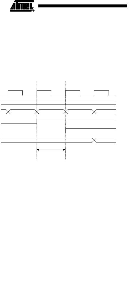
Consider the clock period starting shortly after the first falling edge of the system clock. The latch is closed when the clock is low, and goes transparent when the clock is high, as indicated by the shaded region of the “SYNC LATCH” signal. The signal value is latched when the system clock goes low. It is clocked into the PINxn Register at the succeeding positive clock edge. As indicated by the two arrows tpd,max and tpd,min, a single signal transition on the pin will be delayed between ½ and 1½ system clock period depending upon the time of assertion.
When reading back a software assigned pin value, a nop instruction must be inserted as indicated in Figure 10-4. The out instruction sets the “SYNC LATCH” signal at the positive edge of the clock. In this case, the delay tpd through the synchronizer is one system clock period.
Figure 10-4. Synchronization when Reading a Software Assigned Pin Value
SYSTEM CLK
r16
INSTRUCTIONS
SYNC LATCH
PINxn
r17
0xFF
out PORTx, r16 |
nop |
in r17, PINx |
0x00 |
0xFF |
tpd
The following code example shows how to set port B pins 0 and 1 high, 2 and 3 low, and define the port pins from 4 to 5 as input with a pull-up assigned to port pin 4. The resulting pin values are read back again, but as previously discussed, a nop instruction is included to be able to read back the value recently assigned to some of the pins.
50 ATtiny25/45/85 Auto 
7598C–AVR–09/06