
- •Features
- •1. Pin Configurations
- •2. Overview
- •2.1 Block Diagram
- •2.2 Automotive Quality Grade
- •2.3 Pin Descriptions
- •2.3.3 Port B (PB5..PB0)
- •2.3.4 RESET
- •3. About Code Examples
- •4. AVR CPU Core
- •4.1 Introduction
- •4.2 Architectural Overview
- •4.4 Status Register
- •4.5 General Purpose Register File
- •4.6 Stack Pointer
- •4.7 Instruction Execution Timing
- •4.8 Reset and Interrupt Handling
- •4.8.1 Interrupt Response Time
- •5. AVR ATtiny25/45/85 Memories
- •5.2 SRAM Data Memory
- •5.2.1 Data Memory Access Times
- •5.3 EEPROM Data Memory
- •5.3.1 EEPROM Read/Write Access
- •5.3.6 Atomic Byte Programming
- •5.3.7 Split Byte Programming
- •5.3.8 Erase
- •5.3.9 Write
- •5.3.10 Preventing EEPROM Corruption
- •5.4 I/O Memory
- •6. System Clock and Clock Options
- •6.1 Clock Systems and their Distribution
- •6.2 Clock Sources
- •6.3 Default Clock Source
- •6.4 Crystal Oscillator
- •6.6 Calibrated Internal RC Oscillator
- •6.7 External Clock
- •6.8 128 kHz Internal Oscillator
- •6.9 Clock Output Buffer
- •6.10 System Clock Prescaler
- •6.10.2 Switching Time
- •7. Power Management and Sleep Modes
- •7.1 Idle Mode
- •7.2 ADC Noise Reduction Mode
- •7.4 Power Reduction Register
- •7.5 Minimizing Power Consumption
- •7.5.1 Analog to Digital Converter
- •7.5.2 Analog Comparator
- •7.5.4 Internal Voltage Reference
- •7.5.5 Watchdog Timer
- •7.5.6 Port Pins
- •8. System Control and Reset
- •8.0.1 Resetting the AVR
- •8.0.2 Reset Sources
- •8.0.3 Power-on Reset
- •8.0.4 External Reset
- •8.0.6 Watchdog Reset
- •8.1 Internal Voltage Reference
- •8.2 Watchdog Timer
- •8.3 Timed Sequences for Changing the Configuration of the Watchdog Timer
- •8.3.1 Safety Level 1
- •8.3.2 Safety Level 2
- •9. Interrupts
- •9.1 Interrupt Vectors in ATtiny25/45/85
- •10. I/O Ports
- •10.1 Introduction
- •10.2 Ports as General Digital I/O
- •10.2.1 Configuring the Pin
- •10.2.2 Toggling the Pin
- •10.2.3 Switching Between Input and Output
- •10.2.4 Reading the Pin Value
- •10.2.5 Digital Input Enable and Sleep Modes
- •10.2.6 Unconnected Pins
- •10.3 Alternate Port Functions
- •10.3.2 Alternate Functions of Port B
- •11. External Interrupts
- •12. 8-bit Timer/Counter0 with PWM
- •12.1 Overview
- •12.1.1 Registers
- •12.1.2 Definitions
- •12.2 Timer/Counter Clock Sources
- •12.3 Counter Unit
- •12.4 Output Compare Unit
- •12.4.1 Force Output Compare
- •12.4.2 Compare Match Blocking by TCNT0 Write
- •12.4.3 Using the Output Compare Unit
- •12.5 Compare Match Output Unit
- •12.5.1 Compare Output Mode and Waveform Generation
- •12.6 Modes of Operation
- •12.6.1 Normal Mode
- •12.6.2 Clear Timer on Compare Match (CTC) Mode
- •12.6.3 Fast PWM Mode
- •12.6.4 Phase Correct PWM Mode
- •12.7 Timer/Counter Timing Diagrams
- •13. Timer/Counter Prescaler
- •13.0.1 Prescaler Reset
- •13.0.2 External Clock Source
- •14. 8-bit Timer/Counter1
- •14.1 Timer/Counter1
- •14.1.1 Timer/Counter1 Control Register - TCCR1
- •14.1.2 General Timer/Counter1 Control Register - GTCCR
- •14.1.3 Timer/Counter1 - TCNT1
- •14.1.4 Timer/Counter1 Output Compare RegisterA - OCR1A
- •14.1.5 Timer/Counter1 Output Compare RegisterB - OCR1B
- •14.1.6 Timer/Counter1 Output Compare RegisterC - OCR1C
- •14.1.7 Timer/Counter Interrupt Mask Register - TIMSK
- •14.1.8 Timer/Counter Interrupt Flag Register - TIFR
- •14.1.9 PLL Control and Status Register - PLLCSR
- •14.1.10 Timer/Counter1 Initialization for Asynchronous Mode
- •14.1.11 Timer/Counter1 in PWM Mode
- •15. 8-bit Timer/Counter1 in ATtiny15 Mode
- •15.1 Timer/Counter1 Prescaler
- •15.2 Timer/Counter1
- •15.2.2 Timer/Counter1 Control Register - TCCR1
- •15.2.3 General Timer/Counter1 Control Register - GTCCR
- •15.2.4 Timer/Counter1 - TCNT1
- •15.2.5 Timer/Counter1 Output Compare RegisterA - OCR1A
- •15.2.6 Timer/Counter1 Output Compare Register C - OCR1C
- •15.2.7 Timer/Counter Interrupt Flag Register - TIFR
- •15.2.8 PLL Control and Status Register - PLLCSR
- •15.2.9 Timer/Counter1 in PWM Mode
- •16. Dead Time Generator
- •16.0.1 Timer/Counter1 Dead Time Prescaler register 1 - DTPS1
- •16.0.2 Timer/Counter1 Dead Time A - DT1A
- •16.0.3 Timer/Counter1 Dead Time B - DT1B
- •17.1 Overview
- •17.2 Functional Descriptions
- •17.2.2 SPI Master Operation Example
- •17.2.3 SPI Slave Operation Example
- •17.2.5 Start Condition Detector
- •17.3 Alternative USI Usage
- •17.3.4 Edge Triggered External Interrupt
- •17.3.5 Software Interrupt
- •17.4 USI Register Descriptions
- •18. Analog Comparator
- •18.1 Analog Comparator Multiplexed Input
- •19. Analog to Digital Converter
- •19.1 Features
- •19.2 Operation
- •19.3 Starting a Conversion
- •19.4 Prescaling and Conversion Timing
- •19.5 Changing Channel or Reference Selection
- •19.5.1 ADC Input Channels
- •19.5.2 ADC Voltage Reference
- •19.6 ADC Noise Canceler
- •19.6.1 Analog Input Circuitry
- •19.6.2 Analog Noise Canceling Techniques
- •19.6.3 ADC Accuracy Definitions
- •19.7 ADC Conversion Result
- •19.7.1 Single Ended Conversion
- •19.7.2 Unipolar Differential Conversion
- •19.7.3 Bipolar Differential Conversion
- •19.7.4 Temperature Measurement (Preliminary description)
- •19.7.7.1 ADLAR = 0
- •19.7.7.2 ADLAR = 1
- •20. debugWIRE On-chip Debug System
- •20.1 Features
- •20.2 Overview
- •20.3 Physical Interface
- •20.4 Software Break Points
- •20.5 Limitations of debugWIRE
- •20.6 debugWIRE Related Register in I/O Memory
- •21. Self-Programming the Flash
- •21.0.1 Performing Page Erase by SPM
- •21.0.2 Filling the Temporary Buffer (Page Loading)
- •21.0.3 Performing a Page Write
- •21.1.2 EEPROM Write Prevents Writing to SPMCSR
- •21.1.3 Reading the Fuse and Lock Bits from Software
- •21.1.4 Preventing Flash Corruption
- •21.1.5 Programming Time for Flash when Using SPM
- •22. Memory Programming
- •22.1 Program And Data Memory Lock Bits
- •22.2 Fuse Bytes
- •22.2.1 Latching of Fuses
- •22.3 Signature Bytes
- •22.3.1 ATtiny25 Signature Bytes
- •22.3.2 ATtiny45 Signature Bytes
- •22.3.3 ATtiny85 Signature Bytes
- •22.4 Calibration Byte
- •22.5 Page Size
- •22.6 Serial Downloading
- •22.6.1 Serial Programming Algorithm
- •22.6.2 Serial Programming Characteristics
- •22.7 High-voltage Serial Programming
- •22.8.2 Considerations for Efficient Programming
- •22.8.3 Chip Erase
- •22.8.4 Programming the Flash
- •22.8.5 Programming the EEPROM
- •22.8.6 Reading the Flash
- •22.8.7 Reading the EEPROM
- •22.8.8 Programming and Reading the Fuse and Lock Bits
- •22.8.9 Reading the Signature Bytes and Calibration Byte
- •23. Electrical Characteristics
- •23.1 Absolute Maximum Ratings*
- •23.2 External Clock Drive Waveforms
- •23.3 External Clock Drive
- •23.5 Calibrated RC Oscillator Accuracy
- •24. Typical Characteristics
- •24.1 Active Supply Current
- •24.2 Idle Supply Current
- •24.2.1 Using the Power Reduction Register
- •24.2.1.1 Example 1
- •24.5 Pin Driver Strength
- •24.6 Pin Thresholds and Hysteresis
- •24.7 BOD Thresholds and Analog Comparator Offset
- •24.8 Internal Oscillator Speed
- •24.9 Current Consumption of Peripheral Units
- •24.10 Current Consumption in Reset and Reset Pulse width
- •24.11 Analog to Digital Converter
- •25. Register Summary
- •26. Instruction Set Summary
- •27. Ordering Information
- •28. Packaging Information
- •29. Document Revision History
- •30. Errata
- •30.1 ATtiny25/45/85 Rev. A

ATtiny25/45/85 Auto
6.6.1Oscillator Calibration Register – OSCCAL
Bit |
7 |
6 |
5 |
4 |
3 |
2 |
1 |
0 |
|
|
CAL7 |
CAL6 |
CAL5 |
CAL4 |
CAL3 |
CAL2 |
CAL1 |
CAL0 |
OSCCAL |
|
|
|
|
|
|
|
|
|
|
Read/Write |
R |
R/W |
R/W |
R/W |
R/W |
R/W |
R/W |
R/W |
|
Initial Value |
0 |
|
|
Device Specific Calibration Value |
|
|
|
• Bits 7..0 – CAL7..0: Oscillator Calibration Value
Writing the calibration byte to this address will trim the internal Oscillator to remove process variations from the Oscillator frequency. This is done automatically during Chip Reset. When OSCCAL is zero, the lowest available frequency is chosen. Writing non-zero values to this register will increase the frequency of the internal Oscillator. Writing 0xFF to the register gives the highest available frequency. The calibrated Oscillator is used to time EEPROM and Flash access. If EEPROM or Flash is written, do not calibrate to more than 8.8 MHz frequency. Otherwise, the EEPROM or Flash write may fail.
The CAL7 bit determines the range of operation for the oscillator. Setting this bit to 0 gives the lowest frequency range, setting this bit to 1 gives the highest frequency range. The two frequency ranges are overlapping, in other words a setting of OSCCAL = 0x7F gives a higher frequency than OSCCAL = 0x80.
The CAL6..0 bits are used to tune the frequency within the selected range. A setting of 0x00 gives the lowest frequency in that range, and a setting of 0x7F gives the highest frequency in the range. Incrementing CAL6..0 by 1 will give a frequency increment of less than 2% in the frequency range 7.3 - 8.1 MHz.
Avoid changing the calibration value in large steps when calibrating the calibrated internal RC Oscillator to ensure stable operation of the MCU. A variation in frequency of more than 2% from one cycle to the next can lead to unpredicatble behavior. Changes in OSCCAL should not exceed 0x20 for each calibration. It is required to ensure that the MCU is kept in Reset during such changes in the clock frequency
Table 6-9. |
Internal RC Oscillator Frequency Range |
|
|
|
|
Min Frequency in Percentage of |
Max Frequency in Percentage of |
OSCCAL Value |
Nominal Frequency |
Nominal Frequency |
|
|
|
|
|
0x00 |
|
50% |
100% |
|
|
|
|
0x3F |
|
75% |
150% |
|
|
|
|
0x7F |
|
100% |
200% |
|
|
|
|
6.7External Clock
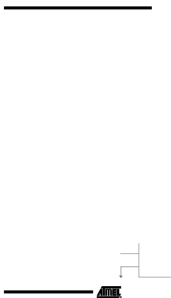
To drive the device from an external clock source, CLKI should be driven as shown in Figure 6- 4. To run the device on an external clock, the CKSEL Fuses must be programmed to “00”.
Figure 6-4. External Clock Drive Configuration
EXTERNAL
CLOCK CLKI
SIGNAL
GND
27
7598C–AVR–09/06