

- •Features
- •1. Pin Configurations
- •1.1 Disclaimer
- •2. Overview
- •2.1 Block Diagram
- •2.2 Pin Descriptions
- •2.2.3 AVCC
- •2.2.4 AGND
- •2.2.5 Port A (PA7..PA0)
- •2.2.6 Port B (PB7..PB0)
- •2.2.7 RESET
- •3. Resources
- •4. About Code Examples
- •5. AVR CPU Core
- •5.1 Overview
- •5.3 Status Register
- •5.4 General Purpose Register File
- •5.5 Stack Pointer
- •5.6 Instruction Execution Timing
- •5.7 Reset and Interrupt Handling
- •5.7.1 Interrupt Response Time
- •6. AVR Memories
- •6.2 SRAM Data Memory
- •6.2.1 Data Memory Access Times
- •6.3 EEPROM Data Memory
- •6.3.1 EEPROM Read/Write Access
- •6.3.2 Atomic Byte Programming
- •6.3.3 Split Byte Programming
- •6.3.4 Erase
- •6.3.5 Write
- •6.3.6 Preventing EEPROM Corruption
- •6.4 I/O Memory
- •6.4.1 General Purpose I/O Registers
- •6.5 Register Description
- •7. System Clock and Clock Options
- •7.1 Clock Systems and their Distribution
- •7.2 Clock Sources
- •7.3 Default Clock Source
- •7.4 External Clock
- •7.6 Calibrated Internal RC Oscillator
- •7.7 128 kHz Internal Oscillator
- •7.9 Crystal Oscillator
- •7.10 Clock Output Buffer
- •7.11 System Clock Prescaler
- •7.11.1 Switching Time
- •7.12 Register Description
- •8. Power Management and Sleep Modes
- •8.1 Sleep Modes
- •8.2 Idle Mode
- •8.3 ADC Noise Reduction Mode
- •8.5 Standby Mode
- •8.6 Power Reduction Register
- •8.7 Minimizing Power Consumption
- •8.7.1 Analog to Digital Converter
- •8.7.2 Analog Comparator
- •8.7.4 Internal Voltage Reference
- •8.7.5 Watchdog Timer
- •8.7.6 Port Pins
- •8.8 Register Description
- •9. System Control and Reset
- •9.0.1 Resetting the AVR
- •9.0.2 Reset Sources
- •9.0.4 External Reset
- •9.0.6 Watchdog Reset
- •9.1 Internal Voltage Reference
- •9.2 Watchdog Timer
- •9.3 Timed Sequences for Changing the Configuration of the Watchdog Timer
- •9.3.1 Safety Level 1
- •9.3.2 Safety Level 2
- •9.4 Register Description
- •10. Interrupts
- •10.1 Interrupt Vectors in ATtiny261/461/861
- •11. External Interrupts
- •11.1 Register Description
- •12. I/O Ports
- •12.1 Overview
- •12.2 Ports as General Digital I/O
- •12.2.1 Configuring the Pin
- •12.2.2 Toggling the Pin
- •12.2.3 Switching Between Input and Output
- •12.2.4 Reading the Pin Value
- •12.2.5 Digital Input Enable and Sleep Modes
- •12.2.6 Unconnected Pins
- •12.3 Alternate Port Functions
- •12.3.1 Alternate Functions of Port B
- •12.3.2 Alternate Functions of Port A
- •12.4 Register Description
- •13. Timer/Counter0 Prescaler
- •13.0.1 Prescaler Reset
- •13.0.2 External Clock Source
- •13.1 Register Description
- •14. Timer/Counter0
- •14.1 Features
- •14.2 Overview
- •14.2.1 Registers
- •14.2.2 Definitions
- •14.3 Timer/Counter Clock Sources
- •14.4 Counter Unit
- •14.5 Modes of Operation
- •14.5.1 Normal 8-bit Mode
- •14.6 Input Capture Unit
- •14.6.1 Input Capture Trigger Source
- •14.6.2 Noise Canceler
- •14.6.3 Using the Input Capture Unit
- •14.7 Output Compare Unit
- •14.7.1 Compare Match Blocking by TCNT0 Write
- •14.7.2 Using the Output Compare Unit
- •14.8 Timer/Counter Timing Diagrams
- •14.9.1 Reusing the temporary high byte register
- •14.10 Register Description
- •15. Timer/Counter1 Prescaler
- •15.0.1 Prescaler Reset
- •15.0.2 Prescaler Initialization for Asynchronous Mode
- •15.1 Register Description
- •16. Timer/Counter1
- •16.1 Features
- •16.2 Overview
- •16.2.1 Speed
- •16.2.2 Accuracy
- •16.2.3 Registers
- •16.2.4 Synchronization
- •16.2.5 Definitions
- •16.3 Counter Unit
- •16.3.1 Counter Initialization for Asynchronous Mode
- •16.4 Output Compare Unit
- •16.4.1 Force Output Compare
- •16.4.2 Compare Match Blocking by TCNT1 Write
- •16.4.3 Using the Output Compare Unit
- •16.5 Dead Time Generator
- •16.6 Compare Match Output Unit
- •16.6.1 Compare Output Mode and Waveform Generation
- •16.7 Modes of Operation
- •16.7.1 Normal Mode
- •16.7.3 Phase and Frequency Correct PWM Mode
- •16.7.4 PWM6 Mode
- •16.8 Timer/Counter Timing Diagrams
- •16.9 Fault Protection Unit
- •16.9.1 Fault Protection Trigger Source
- •16.9.2 Noise Canceler
- •16.10 Accessing 10-Bit Registers
- •16.10.1 Reusing the temporary high byte register
- •16.11 Register Description
- •17.1 Features
- •17.2 Overview
- •17.3 Functional Descriptions
- •17.3.2 SPI Master Operation Example
- •17.3.3 SPI Slave Operation Example
- •17.3.5 Start Condition Detector
- •17.4 Alternative USI Usage
- •17.4.4 Edge Triggered External Interrupt
- •17.4.5 Software Interrupt
- •17.5 Register Descriptions
- •18.1 Register Description
- •18.2 Analog Comparator Multiplexed Input
- •19.1 Features
- •19.2 Overview
- •19.3 Operation
- •19.4 Starting a Conversion
- •19.5 Prescaling and Conversion Timing
- •19.6 Changing Channel or Reference Selection
- •19.6.1 ADC Input Channels
- •19.6.2 ADC Voltage Reference
- •19.7 ADC Noise Canceler
- •19.7.1 Analog Input Circuitry
- •19.7.2 Analog Noise Canceling Techniques
- •19.7.3 ADC Accuracy Definitions
- •19.8 ADC Conversion Result
- •19.8.1 Single Ended Conversion
- •19.8.2 Unipolar Differential Conversion
- •19.8.3 Bipolar Differential Conversion
- •19.9 Temperature Measurement
- •19.10 Register Descriptin
- •19.10.3.1 ADLAR = 0
- •19.10.3.2 ADLAR = 1
- •20. debugWIRE On-chip Debug System
- •20.1 Features
- •20.2 Overview
- •20.3 Physical Interface
- •20.4 Software Break Points
- •20.5 Limitations of debugWIRE
- •20.6 Register Description
- •21. Self-Programming the Flash
- •21.0.1 Performing Page Erase by SPM
- •21.0.2 Filling the Temporary Buffer (Page Loading)
- •21.0.3 Performing a Page Write
- •21.1.1 EEPROM Write Prevents Writing to SPMCSR
- •21.1.2 Reading the Fuse and Lock Bits from Software
- •21.1.3 Preventing Flash Corruption
- •21.1.4 Programming Time for Flash when Using SPM
- •21.2 Register Description
- •22. Memory Programming
- •22.1 Program And Data Memory Lock Bits
- •22.2 Fuse Bytes
- •22.2.1 Latching of Fuses
- •22.3 Signature Bytes
- •22.4 Calibration Byte
- •22.5 Page Size
- •22.6 Parallel Programming Parameters, Pin Mapping, and Commands
- •22.6.1 Signal Names
- •22.7 Parallel Programming
- •22.7.1 Enter Programming Mode
- •22.7.2 Considerations for Efficient Programming
- •22.7.3 Chip Erase
- •22.7.4 Programming the Flash
- •22.7.5 Programming the EEPROM
- •22.7.6 Reading the Flash
- •22.7.7 Reading the EEPROM
- •22.7.8 Programming the Fuse Low Bits
- •22.7.9 Programming the Fuse High Bits
- •22.7.10 Programming the Extended Fuse Bits
- •22.7.11 Programming the Lock Bits
- •22.7.12 Reading the Fuse and Lock Bits
- •22.7.13 Reading the Signature Bytes
- •22.7.14 Reading the Calibration Byte
- •22.8 Serial Downloading
- •22.8.1 Serial Programming Algorithm
- •22.8.2 Serial Programming Instruction set
- •23. Electrical Characteristics
- •23.1 Absolute Maximum Ratings*
- •23.2 DC Characteristics
- •23.3 Speed Grades
- •23.4 Clock Characteristics
- •23.4.1 Calibrated Internal RC Oscillator Accuracy
- •23.4.2 External Clock Drive Waveforms
- •23.4.3 External Clock Drive
- •23.5 System and Reset Characteristics
- •23.7 Parallel Programming Characteristics
- •23.8 Serial Programming Characteristics
- •24. Typical Characteristics
- •24.1 Active Supply Current
- •24.2 Idle Supply Current
- •24.3 Supply Current of I/O modules
- •Example
- •24.6 Pin Driver Strength
- •24.7 Pin Threshold and Hysteresis
- •24.8 BOD Threshold and Analog Comparator Offset
- •24.9 Internal Oscillator Speed
- •24.10 Current Consumption of Peripheral Units
- •24.11 Current Consumption in Reset and Reset Pulsewidth
- •25. Register Summary
- •26. Instruction Set Summary
- •27. Ordering Information
- •27.1 ATtiny261
- •27.2 ATtiny461
- •27.3 ATtiny861
- •28. Packaging Information
- •29. Errata
- •29.1 Errata ATtiny261
- •29.2 Errata ATtiny461
- •29.3 Errata ATtiny861
- •30. Datasheet Revision History
- •Table of Contents
ATtiny261/461/861
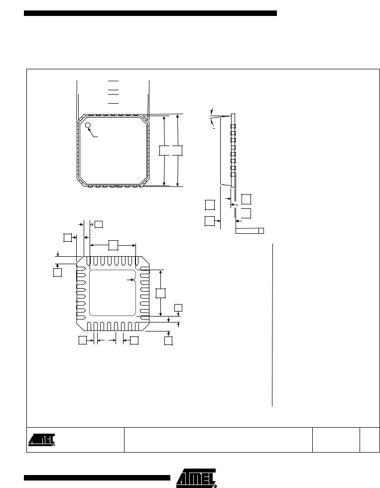
28. Packaging Information
28.132M1-A

 D
D 


 D1
D1 

1 |
0 |
|
2 |
||
Pin 1 ID |
||
3 |
E1 
 E
E
TOP VIEW
A2 
A
 K
K
P |
|
|
D2 |
|
|
P |
1 |
|
2 |
||
Pin #1 Notch |
||
|
(0.20 R) 3
E2
K
b |
e |
L |
BOTTOM VIEW
Note: JEDEC Standard MO-220, Fig. 2 (Anvil Singulation), VHHD-2.
SIDE VIEW
 A3
A3


 A1
A1

 0.08 C COMMON DIMENSIONS
(Unit of Measure = mm)
SYMBOL |
MIN |
NOM |
MAX |
NOTE |
A |
0.80 |
0.90 |
1.00 |
|
|
|
|
|
|
A1 |
– |
0.02 |
0.05 |
|
|
|
|
|
|
A2 |
– |
0.65 |
1.00 |
|
|
|
|
|
|
A3 |
|
0.20 REF |
|
|
|
|
|
|
|
b |
0.18 |
0.23 |
0.30 |
|
|
|
|
|
|
D |
|
5.00 BSC |
|
|
|
|
|
|
|
D1 |
|
4.75 BSC |
|
|
|
|
|
|
|
D2 |
2.95 |
3.10 |
3.25 |
|
|
|
|
|
|
E |
|
5.00 BSC |
|
|
|
|
|
|
|
E1 |
|
4.75BSC |
|
|
|
|
|
|
|
E2 |
2.95 |
3.10 |
3.25 |
|
|
|
|
|
|
e |
|
0.50 BSC |
|
|
|
|
|
|
|
L |
0.30 |
0.40 |
0.50 |
|
|
|
|
|
|
P |
– |
– |
0.60 |
|
|
|
|
|
|
0 |
– |
– |
12o |
|
K |
0.20 |
– |
– |
|
|
|
|
|
|
8/19/04
TITLE
|
2325 Orchard Parkway |
32M1-A, 32-pad, 5 x 5 x 1.0 mm Body, Lead Pitch 0.50 mm, |
|
San Jose, CA 95131 |
|
R |
3.10 mm Exposed Pad, Micro Lead Frame Package (MLF) |
DRAWING NO. REV.
32M1-A D
225
2588B–AVR–11/06

28.220P3
D
PIN 1
E1
A
SEATING PLANE
A1
L
B
B1
e
E
C 
 eC
eC
eB
Notes: 1. This package conforms to JEDEC reference MS-001, Variation AD.
2.Dimensions D and E1 do not include mold Flash or Protrusion. Mold Flash or Protrusion shall not exceed 0.25 mm (0.010").
COMMON DIMENSIONS
(Unit of Measure = mm)
SYMBOL |
MIN |
NOM |
MAX |
NOTE |
A |
– |
– |
5.334 |
|
A1 |
0.381 |
– |
– |
|
D |
25.493 |
– |
25.984 |
Note 2 |
E |
7.620 |
– |
8.255 |
|
E1 |
6.096 |
– |
7.112 |
Note 2 |
B |
0.356 |
– |
0.559 |
|
B1 |
1.270 |
– |
1.551 |
|
L |
2.921 |
– |
3.810 |
|
C |
0.203 |
– |
0.356 |
|
eB |
– |
– |
10.922 |
|
eC |
0.000 |
– |
1.524 |
|
|
|
|
|
|
e |
|
2.540 TYP |
|
|
TITLE
|
2325 Orchard Parkway |
20P3, 20-lead (0.300"/7.62 mm Wide) Plastic Dual |
|
San Jose, CA 95131 |
|
R |
Inline Package (PDIP) |
1/12/04
DRAWING NO. REV.
20P3 C
226 ATtiny261/461/861
2588B–AVR–11/06

ATtiny261/461/861
28.320S2
227
2588B–AVR–11/06