

- •Features
- •1. Pin Configurations
- •1.1 Pin Descriptions
- •1.1.3 Port B (PB7:0) XTAL1/XTAL2/TOSC1/TOSC2
- •1.1.4 Port C (PC5:0)
- •1.1.5 PC6/RESET
- •1.1.6 Port D (PD7:0)
- •1.1.8 AREF
- •1.1.9 ADC7:6 (TQFP and QFN/MLF Package Only)
- •2. Overview
- •2.1 Block Diagram
- •2.2 Comparison Between ATmega48, ATmega88, and ATmega168
- •3. Resources
- •4. Data Retention
- •5. About Code Examples
- •6. AVR CPU Core
- •6.1 Overview
- •6.2 Architectural Overview
- •6.4 Status Register
- •6.5 General Purpose Register File
- •6.6 Stack Pointer
- •6.7 Instruction Execution Timing
- •6.8 Reset and Interrupt Handling
- •6.8.1 Interrupt Response Time
- •7. AVR Memories
- •7.1 Overview
- •7.3 SRAM Data Memory
- •7.3.1 Data Memory Access Times
- •7.4 EEPROM Data Memory
- •7.4.1 EEPROM Read/Write Access
- •7.4.2 Preventing EEPROM Corruption
- •7.5 I/O Memory
- •7.5.1 General Purpose I/O Registers
- •7.6 Register Description
- •8. System Clock and Clock Options
- •8.1 Clock Systems and their Distribution
- •8.2 Clock Sources
- •8.2.1 Default Clock Source
- •8.2.2 Clock Startup Sequence
- •8.3 Low Power Crystal Oscillator
- •8.4 Full Swing Crystal Oscillator
- •8.5 Low Frequency Crystal Oscillator
- •8.6 Calibrated Internal RC Oscillator
- •8.7 128 kHz Internal Oscillator
- •8.8 External Clock
- •8.9 Clock Output Buffer
- •8.10 Timer/Counter Oscillator
- •8.11 System Clock Prescaler
- •8.12 Register Description
- •9. Power Management and Sleep Modes
- •9.1 Sleep Modes
- •9.2 Idle Mode
- •9.3 ADC Noise Reduction Mode
- •9.4 Power-down Mode
- •9.5 Power-save Mode
- •9.6 Standby Mode
- •9.7 Power Reduction Register
- •9.8 Minimizing Power Consumption
- •9.8.1 Analog to Digital Converter
- •9.8.2 Analog Comparator
- •9.8.4 Internal Voltage Reference
- •9.8.5 Watchdog Timer
- •9.8.6 Port Pins
- •9.9 Register Description
- •10. System Control and Reset
- •10.1 Resetting the AVR
- •10.2 Reset Sources
- •10.3 Power-on Reset
- •10.4 External Reset
- •10.6 Watchdog System Reset
- •10.7 Internal Voltage Reference
- •10.8 Watchdog Timer
- •10.8.1 Features
- •10.9 Register Description
- •11. Interrupts
- •11.1 Overview
- •11.2 Interrupt Vectors in ATmega48
- •11.3 Interrupt Vectors in ATmega88
- •11.4 Interrupt Vectors in ATmega168
- •11.4.1 Moving Interrupts Between Application and Boot Space, ATmega88 and ATmega168
- •11.5 Register Description
- •12. External Interrupts
- •12.1 Pin Change Interrupt Timing
- •12.2 Register Description
- •13. I/O-Ports
- •13.1 Overview
- •13.2 Ports as General Digital I/O
- •13.2.1 Configuring the Pin
- •13.2.2 Toggling the Pin
- •13.2.3 Switching Between Input and Output
- •13.2.4 Reading the Pin Value
- •13.2.5 Digital Input Enable and Sleep Modes
- •13.2.6 Unconnected Pins
- •13.3 Alternate Port Functions
- •13.3.1 Alternate Functions of Port B
- •13.3.2 Alternate Functions of Port C
- •13.3.3 Alternate Functions of Port D
- •13.4 Register Description
- •14. 8-bit Timer/Counter0 with PWM
- •14.1 Features
- •14.2 Overview
- •14.2.1 Definitions
- •14.2.2 Registers
- •14.3 Timer/Counter Clock Sources
- •14.4 Counter Unit
- •14.5 Output Compare Unit
- •14.5.1 Force Output Compare
- •14.5.2 Compare Match Blocking by TCNT0 Write
- •14.5.3 Using the Output Compare Unit
- •14.6 Compare Match Output Unit
- •14.6.1 Compare Output Mode and Waveform Generation
- •14.7 Modes of Operation
- •14.7.1 Normal Mode
- •14.7.2 Clear Timer on Compare Match (CTC) Mode
- •14.7.3 Fast PWM Mode
- •14.7.4 Phase Correct PWM Mode
- •14.8 Timer/Counter Timing Diagrams
- •14.9 Register Description
- •15. 16-bit Timer/Counter1 with PWM
- •15.1 Features
- •15.2 Overview
- •15.2.1 Registers
- •15.2.2 Definitions
- •15.3.1 Reusing the Temporary High Byte Register
- •15.4 Timer/Counter Clock Sources
- •15.5 Counter Unit
- •15.6 Input Capture Unit
- •15.6.1 Input Capture Trigger Source
- •15.6.2 Noise Canceler
- •15.6.3 Using the Input Capture Unit
- •15.7 Output Compare Units
- •15.7.1 Force Output Compare
- •15.7.2 Compare Match Blocking by TCNT1 Write
- •15.7.3 Using the Output Compare Unit
- •15.8 Compare Match Output Unit
- •15.8.1 Compare Output Mode and Waveform Generation
- •15.9 Modes of Operation
- •15.9.1 Normal Mode
- •15.9.2 Clear Timer on Compare Match (CTC) Mode
- •15.9.3 Fast PWM Mode
- •15.9.4 Phase Correct PWM Mode
- •15.9.5 Phase and Frequency Correct PWM Mode
- •15.10 Timer/Counter Timing Diagrams
- •15.11 Register Description
- •16. Timer/Counter0 and Timer/Counter1 Prescalers
- •16.0.1 Internal Clock Source
- •16.0.2 Prescaler Reset
- •16.0.3 External Clock Source
- •16.1 Register Description
- •17. 8-bit Timer/Counter2 with PWM and Asynchronous Operation
- •17.1 Features
- •17.2 Overview
- •17.2.1 Registers
- •17.2.2 Definitions
- •17.3 Timer/Counter Clock Sources
- •17.4 Counter Unit
- •17.5 Output Compare Unit
- •17.5.1 Force Output Compare
- •17.5.2 Compare Match Blocking by TCNT2 Write
- •17.5.3 Using the Output Compare Unit
- •17.6 Compare Match Output Unit
- •17.6.1 Compare Output Mode and Waveform Generation
- •17.7 Modes of Operation
- •17.7.1 Normal Mode
- •17.7.2 Clear Timer on Compare Match (CTC) Mode
- •17.7.3 Fast PWM Mode
- •17.7.4 Phase Correct PWM Mode
- •17.8 Timer/Counter Timing Diagrams
- •17.9 Asynchronous Operation of Timer/Counter2
- •17.10 Timer/Counter Prescaler
- •17.11 Register Description
- •18.1 Features
- •18.2 Overview
- •18.3 SS Pin Functionality
- •18.3.1 Slave Mode
- •18.3.2 Master Mode
- •18.4 Data Modes
- •18.5 Register Description
- •19. USART0
- •19.1 Features
- •19.2 Overview
- •19.3 Clock Generation
- •19.3.2 Double Speed Operation (U2Xn)
- •19.3.3 External Clock
- •19.3.4 Synchronous Clock Operation
- •19.4 Frame Formats
- •19.4.1 Parity Bit Calculation
- •19.5 USART Initialization
- •19.6.1 Sending Frames with 5 to 8 Data Bit
- •19.6.2 Sending Frames with 9 Data Bit
- •19.6.3 Transmitter Flags and Interrupts
- •19.6.4 Parity Generator
- •19.6.5 Disabling the Transmitter
- •19.7.1 Receiving Frames with 5 to 8 Data Bits
- •19.7.2 Receiving Frames with 9 Data Bits
- •19.7.3 Receive Compete Flag and Interrupt
- •19.7.4 Receiver Error Flags
- •19.7.5 Parity Checker
- •19.7.6 Disabling the Receiver
- •19.7.7 Flushing the Receive Buffer
- •19.8 Asynchronous Data Reception
- •19.8.1 Asynchronous Clock Recovery
- •19.8.2 Asynchronous Data Recovery
- •19.8.3 Asynchronous Operational Range
- •19.9.1 Using MPCMn
- •19.10 Register Description
- •19.11 Examples of Baud Rate Setting
- •20. USART in SPI Mode
- •20.1 Features
- •20.2 Overview
- •20.3 Clock Generation
- •20.4 SPI Data Modes and Timing
- •20.5 Frame Formats
- •20.5.1 USART MSPIM Initialization
- •20.6 Data Transfer
- •20.6.1 Transmitter and Receiver Flags and Interrupts
- •20.6.2 Disabling the Transmitter or Receiver
- •20.7 AVR USART MSPIM vs. AVR SPI
- •20.8 Register Description
- •20.8.5 USART MSPIM Baud Rate Registers - UBRRnL and UBRRnH
- •21. 2-wire Serial Interface
- •21.1 Features
- •21.2.1 TWI Terminology
- •21.2.2 Electrical Interconnection
- •21.3 Data Transfer and Frame Format
- •21.3.1 Transferring Bits
- •21.3.2 START and STOP Conditions
- •21.3.3 Address Packet Format
- •21.3.4 Data Packet Format
- •21.3.5 Combining Address and Data Packets into a Transmission
- •21.5 Overview of the TWI Module
- •21.5.1 SCL and SDA Pins
- •21.5.2 Bit Rate Generator Unit
- •21.5.3 Bus Interface Unit
- •21.5.4 Address Match Unit
- •21.5.5 Control Unit
- •21.6 Using the TWI
- •21.7 Transmission Modes
- •21.7.1 Master Transmitter Mode
- •21.7.2 Master Receiver Mode
- •21.7.3 Slave Receiver Mode
- •21.7.4 Slave Transmitter Mode
- •21.7.5 Miscellaneous States
- •21.7.6 Combining Several TWI Modes
- •21.9 Register Description
- •22. Analog Comparator
- •22.1 Overview
- •22.2 Analog Comparator Multiplexed Input
- •22.3 Register Description
- •23. Analog-to-Digital Converter
- •23.1 Features
- •23.2 Overview
- •23.3 Starting a Conversion
- •23.4 Prescaling and Conversion Timing
- •23.5 Changing Channel or Reference Selection
- •23.5.1 ADC Input Channels
- •23.5.2 ADC Voltage Reference
- •23.6 ADC Noise Canceler
- •23.6.1 Analog Input Circuitry
- •23.6.2 Analog Noise Canceling Techniques
- •23.6.3 ADC Accuracy Definitions
- •23.7 ADC Conversion Result
- •23.8 Register Description
- •23.8.3.1 ADLAR = 0
- •23.8.3.2 ADLAR = 1
- •24. debugWIRE On-chip Debug System
- •24.1 Features
- •24.2 Overview
- •24.3 Physical Interface
- •24.4 Software Break Points
- •24.5 Limitations of debugWIRE
- •24.6 Register Description
- •25. Self-Programming the Flash, ATmega48
- •25.1 Overview
- •25.1.1 Performing Page Erase by SPM
- •25.1.2 Filling the Temporary Buffer (Page Loading)
- •25.1.3 Performing a Page Write
- •25.2.1 EEPROM Write Prevents Writing to SPMCSR
- •25.2.2 Reading the Fuse and Lock Bits from Software
- •25.2.3 Preventing Flash Corruption
- •25.2.4 Programming Time for Flash when Using SPM
- •25.2.5 Simple Assembly Code Example for a Boot Loader
- •25.3 Register Description
- •26.1 Features
- •26.2 Overview
- •26.3 Application and Boot Loader Flash Sections
- •26.3.1 Application Section
- •26.5 Boot Loader Lock Bits
- •26.6 Entering the Boot Loader Program
- •26.8.1 Performing Page Erase by SPM
- •26.8.2 Filling the Temporary Buffer (Page Loading)
- •26.8.3 Performing a Page Write
- •26.8.4 Using the SPM Interrupt
- •26.8.5 Consideration While Updating BLS
- •26.8.7 Setting the Boot Loader Lock Bits by SPM
- •26.8.8 EEPROM Write Prevents Writing to SPMCSR
- •26.8.9 Reading the Fuse and Lock Bits from Software
- •26.8.10 Preventing Flash Corruption
- •26.8.11 Programming Time for Flash when Using SPM
- •26.8.12 Simple Assembly Code Example for a Boot Loader
- •26.8.13 ATmega88 Boot Loader Parameters
- •26.8.14 ATmega168 Boot Loader Parameters
- •26.9 Register Description
- •27. Memory Programming
- •27.1 Program And Data Memory Lock Bits
- •27.2 Fuse Bits
- •27.2.1 Latching of Fuses
- •27.3 Signature Bytes
- •27.4 Calibration Byte
- •27.5 Page Size
- •27.6 Parallel Programming Parameters, Pin Mapping, and Commands
- •27.6.1 Signal Names
- •27.7 Parallel Programming
- •27.7.1 Enter Programming Mode
- •27.7.2 Considerations for Efficient Programming
- •27.7.3 Chip Erase
- •27.7.4 Programming the Flash
- •27.7.5 Programming the EEPROM
- •27.7.6 Reading the Flash
- •27.7.7 Reading the EEPROM
- •27.7.8 Programming the Fuse Low Bits
- •27.7.9 Programming the Fuse High Bits
- •27.7.10 Programming the Extended Fuse Bits
- •27.7.11 Programming the Lock Bits
- •27.7.12 Reading the Fuse and Lock Bits
- •27.7.13 Reading the Signature Bytes
- •27.7.14 Reading the Calibration Byte
- •27.7.15 Parallel Programming Characteristics
- •27.8 Serial Downloading
- •27.8.1 Serial Programming Pin Mapping
- •27.8.2 Serial Programming Algorithm
- •27.8.3 Serial Programming Instruction set
- •27.8.4 SPI Serial Programming Characteristics
- •28. Electrical Characteristics
- •28.1 Absolute Maximum Ratings*
- •28.2 DC Characteristics
- •28.3 Speed Grades
- •28.4 Clock Characteristics
- •28.4.1 Calibrated Internal RC Oscillator Accuracy
- •28.4.2 External Clock Drive Waveforms
- •28.4.3 External Clock Drive
- •28.5 System and Reset Characteristics
- •28.7 SPI Timing Characteristics
- •28.8 ADC Characteristics
- •28.9 Parallel Programming Characteristics
- •29. Typical Characteristics
- •29.1 Active Supply Current
- •29.2 Idle Supply Current
- •29.3 Supply Current of I/O modules
- •29.3.0.1 Example 1
- •29.3.0.2 Example 2
- •29.3.0.3 Example 3
- •29.6 Standby Supply Current
- •29.8 Pin Driver Strength
- •29.9 Pin Thresholds and Hysteresis
- •29.10 BOD Thresholds and Analog Comparator Offset
- •29.11 Internal Oscillator Speed
- •29.12 Current Consumption of Peripheral Units
- •29.13 Current Consumption in Reset and Reset Pulse width
- •30. Register Summary
- •31. Instruction Set Summary
- •32. Ordering Information
- •32.1 ATmega48
- •32.2 ATmega88
- •32.3 ATmega168
- •33. Packaging Information
- •34. Errata
- •34.1 Errata ATmega48
- •34.2 Errata ATmega88
- •34.3 Errata ATmega168
- •35. Datasheet Revision History

26.Boot Loader Support – Read-While-Write Self-Programming, ATmega88 and ATmega168
26.1Features
•Read-While-Write Self-Programming
•Flexible Boot Memory Size
•High Security (Separate Boot Lock Bits for a Flexible Protection)
•Separate Fuse to Select Reset Vector
•Optimized Page(1) Size
•Code Efficient Algorithm
•Efficient Read-Modify-Write Support
Note: 1. A page is a section in the Flash consisting of several bytes (see Table 27-9 on page 290) used during programming. The page organization does not affect normal operation.
26.2Overview
In ATmega88 and ATmega168, the Boot Loader Support provides a real Read-While-Write SelfProgramming mechanism for downloading and uploading program code by the MCU itself. This feature allows flexible application software updates controlled by the MCU using a Flash-resi- dent Boot Loader program. The Boot Loader program can use any available data interface and associated protocol to read code and write (program) that code into the Flash memory, or read the code from the program memory. The program code within the Boot Loader section has the capability to write into the entire Flash, including the Boot Loader memory. The Boot Loader can thus even modify itself, and it can also erase itself from the code if the feature is not needed anymore. The size of the Boot Loader memory is configurable with fuses and the Boot Loader has two separate sets of Boot Lock bits which can be set independently. This gives the user a unique flexibility to select different levels of protection.
26.3Application and Boot Loader Flash Sections
The Flash memory is organized in two main sections, the Application section and the Boot Loader section (see Figure 26-2). The size of the different sections is configured by the BOOTSZ Fuses as shown in Table 26-6 on page 282 and Figure 26-2. These two sections can have different level of protection since they have different sets of Lock bits.
26.3.1Application Section
The Application section is the section of the Flash that is used for storing the application code. The protection level for the Application section can be selected by the application Boot Lock bits (Boot Lock bits 0), see Table 26-2 on page 274. The Application section can never store any Boot Loader code since the SPM instruction is disabled when executed from the Application section.
26.3.2BLS – Boot Loader Section
While the Application section is used for storing the application code, the The Boot Loader software must be located in the BLS since the SPM instruction can initiate a programming when executing from the BLS only. The SPM instruction can access the entire Flash, including the BLS itself. The protection level for the Boot Loader section can be selected by the Boot Loader Lock bits (Boot Lock bits 1), see Table 26-3 on page 274.
270 ATmega48/88/168 
2545M–AVR–09/07
 ATmega48/88/168
26.4Read-While-Write and No Read-While-Write Flash Sections
Whether the CPU supports Read-While-Write or if the CPU is halted during a Boot Loader software update is dependent on which address that is being programmed. In addition to the two sections that are configurable by the BOOTSZ Fuses as described above, the Flash is also divided into two fixed sections, the Read-While-Write (RWW) section and the No Read-While- Write (NRWW) section. The limit between the RWWand NRWW sections is given in Table 26- 7 on page 282 and Figure 26-2 on page 273. The main difference between the two sections is:
•When erasing or writing a page located inside the RWW section, the NRWW section can be read during the operation.
•When erasing or writing a page located inside the NRWW section, the CPU is halted during the entire operation.
Note that the user software can never read any code that is located inside the RWW section during a Boot Loader software operation. The syntax “Read-While-Write section” refers to which section that is being programmed (erased or written), not which section that actually is being read during a Boot Loader software update.
26.4.1RWW – Read-While-Write Section
If a Boot Loader software update is programming a page inside the RWW section, it is possible to read code from the Flash, but only code that is located in the NRWW section. During an ongoing programming, the software must ensure that the RWW section never is being read. If the user software is trying to read code that is located inside the RWW section (i.e., by a call/jmp/lpm or an interrupt) during programming, the software might end up in an unknown state. To avoid this, the interrupts should either be disabled or moved to the Boot Loader section. The Boot Loader section is always located in the NRWW section. The RWW Section Busy bit (RWWSB) in the Store Program Memory Control and Status Register (SPMCSR) will be read as logical one as long as the RWW section is blocked for reading. After a programming is completed, the RWWSB must be cleared by software before reading code located in the RWW section. See “SPMCSR – Store Program Memory Control and Status Register” on page 284. for details on how to clear RWWSB.
26.4.2NRWW – No Read-While-Write Section
The code located in the NRWW section can be read when the Boot Loader software is updating a page in the RWW section. When the Boot Loader code updates the NRWW section, the CPU is halted during the entire Page Erase or Page Write operation.
Table 26-1. Read-While-Write Features
Which Section does the Z- |
Which Section can be |
|
|
pointer Address during |
read during |
|
Read-While-Write |
the Programming? |
Programming? |
CPU Halted? |
Supported? |
|
|
|
|
RWW Section |
NRWW Section |
No |
Yes |
|
|
|
|
NRWW Section |
None |
Yes |
No |
|
|
|
|
271
2545M–AVR–09/07
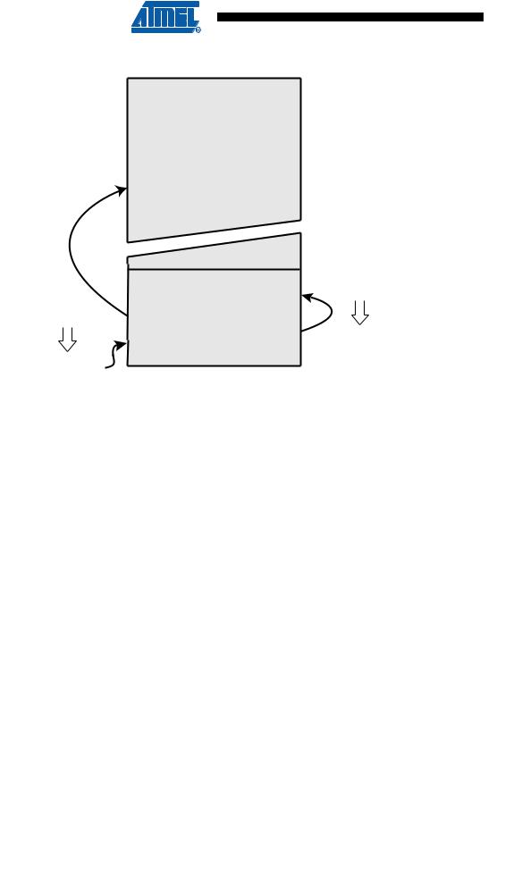
Figure 26-1. Read-While-Write vs. No Read-While-Write
Read-While-Write
(RWW) Section
|
Z-pointer |
|
|
Addresses NRWW |
|
Z-pointer |
Section |
|
No Read-While-Write |
||
Addresses RWW |
||
Section |
(NRWW) Section |
|
|
CPU is Halted |
|
Code Located in |
During the Operation |
|
|
||
NRWW Section |
|
|
Can be Read During |
|
|
the Operation |
|
272 ATmega48/88/168 
2545M–AVR–09/07