

- •Features
- •1. Pin Configurations
- •1.1 Pin Descriptions
- •1.1.3 Port B (PB7:0) XTAL1/XTAL2/TOSC1/TOSC2
- •1.1.4 Port C (PC5:0)
- •1.1.5 PC6/RESET
- •1.1.6 Port D (PD7:0)
- •1.1.8 AREF
- •1.1.9 ADC7:6 (TQFP and QFN/MLF Package Only)
- •2. Overview
- •2.1 Block Diagram
- •2.2 Comparison Between ATmega48, ATmega88, and ATmega168
- •3. Resources
- •4. Data Retention
- •5. About Code Examples
- •6. AVR CPU Core
- •6.1 Overview
- •6.2 Architectural Overview
- •6.4 Status Register
- •6.5 General Purpose Register File
- •6.6 Stack Pointer
- •6.7 Instruction Execution Timing
- •6.8 Reset and Interrupt Handling
- •6.8.1 Interrupt Response Time
- •7. AVR Memories
- •7.1 Overview
- •7.3 SRAM Data Memory
- •7.3.1 Data Memory Access Times
- •7.4 EEPROM Data Memory
- •7.4.1 EEPROM Read/Write Access
- •7.4.2 Preventing EEPROM Corruption
- •7.5 I/O Memory
- •7.5.1 General Purpose I/O Registers
- •7.6 Register Description
- •8. System Clock and Clock Options
- •8.1 Clock Systems and their Distribution
- •8.2 Clock Sources
- •8.2.1 Default Clock Source
- •8.2.2 Clock Startup Sequence
- •8.3 Low Power Crystal Oscillator
- •8.4 Full Swing Crystal Oscillator
- •8.5 Low Frequency Crystal Oscillator
- •8.6 Calibrated Internal RC Oscillator
- •8.7 128 kHz Internal Oscillator
- •8.8 External Clock
- •8.9 Clock Output Buffer
- •8.10 Timer/Counter Oscillator
- •8.11 System Clock Prescaler
- •8.12 Register Description
- •9. Power Management and Sleep Modes
- •9.1 Sleep Modes
- •9.2 Idle Mode
- •9.3 ADC Noise Reduction Mode
- •9.4 Power-down Mode
- •9.5 Power-save Mode
- •9.6 Standby Mode
- •9.7 Power Reduction Register
- •9.8 Minimizing Power Consumption
- •9.8.1 Analog to Digital Converter
- •9.8.2 Analog Comparator
- •9.8.4 Internal Voltage Reference
- •9.8.5 Watchdog Timer
- •9.8.6 Port Pins
- •9.9 Register Description
- •10. System Control and Reset
- •10.1 Resetting the AVR
- •10.2 Reset Sources
- •10.3 Power-on Reset
- •10.4 External Reset
- •10.6 Watchdog System Reset
- •10.7 Internal Voltage Reference
- •10.8 Watchdog Timer
- •10.8.1 Features
- •10.9 Register Description
- •11. Interrupts
- •11.1 Overview
- •11.2 Interrupt Vectors in ATmega48
- •11.3 Interrupt Vectors in ATmega88
- •11.4 Interrupt Vectors in ATmega168
- •11.4.1 Moving Interrupts Between Application and Boot Space, ATmega88 and ATmega168
- •11.5 Register Description
- •12. External Interrupts
- •12.1 Pin Change Interrupt Timing
- •12.2 Register Description
- •13. I/O-Ports
- •13.1 Overview
- •13.2 Ports as General Digital I/O
- •13.2.1 Configuring the Pin
- •13.2.2 Toggling the Pin
- •13.2.3 Switching Between Input and Output
- •13.2.4 Reading the Pin Value
- •13.2.5 Digital Input Enable and Sleep Modes
- •13.2.6 Unconnected Pins
- •13.3 Alternate Port Functions
- •13.3.1 Alternate Functions of Port B
- •13.3.2 Alternate Functions of Port C
- •13.3.3 Alternate Functions of Port D
- •13.4 Register Description
- •14. 8-bit Timer/Counter0 with PWM
- •14.1 Features
- •14.2 Overview
- •14.2.1 Definitions
- •14.2.2 Registers
- •14.3 Timer/Counter Clock Sources
- •14.4 Counter Unit
- •14.5 Output Compare Unit
- •14.5.1 Force Output Compare
- •14.5.2 Compare Match Blocking by TCNT0 Write
- •14.5.3 Using the Output Compare Unit
- •14.6 Compare Match Output Unit
- •14.6.1 Compare Output Mode and Waveform Generation
- •14.7 Modes of Operation
- •14.7.1 Normal Mode
- •14.7.2 Clear Timer on Compare Match (CTC) Mode
- •14.7.3 Fast PWM Mode
- •14.7.4 Phase Correct PWM Mode
- •14.8 Timer/Counter Timing Diagrams
- •14.9 Register Description
- •15. 16-bit Timer/Counter1 with PWM
- •15.1 Features
- •15.2 Overview
- •15.2.1 Registers
- •15.2.2 Definitions
- •15.3.1 Reusing the Temporary High Byte Register
- •15.4 Timer/Counter Clock Sources
- •15.5 Counter Unit
- •15.6 Input Capture Unit
- •15.6.1 Input Capture Trigger Source
- •15.6.2 Noise Canceler
- •15.6.3 Using the Input Capture Unit
- •15.7 Output Compare Units
- •15.7.1 Force Output Compare
- •15.7.2 Compare Match Blocking by TCNT1 Write
- •15.7.3 Using the Output Compare Unit
- •15.8 Compare Match Output Unit
- •15.8.1 Compare Output Mode and Waveform Generation
- •15.9 Modes of Operation
- •15.9.1 Normal Mode
- •15.9.2 Clear Timer on Compare Match (CTC) Mode
- •15.9.3 Fast PWM Mode
- •15.9.4 Phase Correct PWM Mode
- •15.9.5 Phase and Frequency Correct PWM Mode
- •15.10 Timer/Counter Timing Diagrams
- •15.11 Register Description
- •16. Timer/Counter0 and Timer/Counter1 Prescalers
- •16.0.1 Internal Clock Source
- •16.0.2 Prescaler Reset
- •16.0.3 External Clock Source
- •16.1 Register Description
- •17. 8-bit Timer/Counter2 with PWM and Asynchronous Operation
- •17.1 Features
- •17.2 Overview
- •17.2.1 Registers
- •17.2.2 Definitions
- •17.3 Timer/Counter Clock Sources
- •17.4 Counter Unit
- •17.5 Output Compare Unit
- •17.5.1 Force Output Compare
- •17.5.2 Compare Match Blocking by TCNT2 Write
- •17.5.3 Using the Output Compare Unit
- •17.6 Compare Match Output Unit
- •17.6.1 Compare Output Mode and Waveform Generation
- •17.7 Modes of Operation
- •17.7.1 Normal Mode
- •17.7.2 Clear Timer on Compare Match (CTC) Mode
- •17.7.3 Fast PWM Mode
- •17.7.4 Phase Correct PWM Mode
- •17.8 Timer/Counter Timing Diagrams
- •17.9 Asynchronous Operation of Timer/Counter2
- •17.10 Timer/Counter Prescaler
- •17.11 Register Description
- •18.1 Features
- •18.2 Overview
- •18.3 SS Pin Functionality
- •18.3.1 Slave Mode
- •18.3.2 Master Mode
- •18.4 Data Modes
- •18.5 Register Description
- •19. USART0
- •19.1 Features
- •19.2 Overview
- •19.3 Clock Generation
- •19.3.2 Double Speed Operation (U2Xn)
- •19.3.3 External Clock
- •19.3.4 Synchronous Clock Operation
- •19.4 Frame Formats
- •19.4.1 Parity Bit Calculation
- •19.5 USART Initialization
- •19.6.1 Sending Frames with 5 to 8 Data Bit
- •19.6.2 Sending Frames with 9 Data Bit
- •19.6.3 Transmitter Flags and Interrupts
- •19.6.4 Parity Generator
- •19.6.5 Disabling the Transmitter
- •19.7.1 Receiving Frames with 5 to 8 Data Bits
- •19.7.2 Receiving Frames with 9 Data Bits
- •19.7.3 Receive Compete Flag and Interrupt
- •19.7.4 Receiver Error Flags
- •19.7.5 Parity Checker
- •19.7.6 Disabling the Receiver
- •19.7.7 Flushing the Receive Buffer
- •19.8 Asynchronous Data Reception
- •19.8.1 Asynchronous Clock Recovery
- •19.8.2 Asynchronous Data Recovery
- •19.8.3 Asynchronous Operational Range
- •19.9.1 Using MPCMn
- •19.10 Register Description
- •19.11 Examples of Baud Rate Setting
- •20. USART in SPI Mode
- •20.1 Features
- •20.2 Overview
- •20.3 Clock Generation
- •20.4 SPI Data Modes and Timing
- •20.5 Frame Formats
- •20.5.1 USART MSPIM Initialization
- •20.6 Data Transfer
- •20.6.1 Transmitter and Receiver Flags and Interrupts
- •20.6.2 Disabling the Transmitter or Receiver
- •20.7 AVR USART MSPIM vs. AVR SPI
- •20.8 Register Description
- •20.8.5 USART MSPIM Baud Rate Registers - UBRRnL and UBRRnH
- •21. 2-wire Serial Interface
- •21.1 Features
- •21.2.1 TWI Terminology
- •21.2.2 Electrical Interconnection
- •21.3 Data Transfer and Frame Format
- •21.3.1 Transferring Bits
- •21.3.2 START and STOP Conditions
- •21.3.3 Address Packet Format
- •21.3.4 Data Packet Format
- •21.3.5 Combining Address and Data Packets into a Transmission
- •21.5 Overview of the TWI Module
- •21.5.1 SCL and SDA Pins
- •21.5.2 Bit Rate Generator Unit
- •21.5.3 Bus Interface Unit
- •21.5.4 Address Match Unit
- •21.5.5 Control Unit
- •21.6 Using the TWI
- •21.7 Transmission Modes
- •21.7.1 Master Transmitter Mode
- •21.7.2 Master Receiver Mode
- •21.7.3 Slave Receiver Mode
- •21.7.4 Slave Transmitter Mode
- •21.7.5 Miscellaneous States
- •21.7.6 Combining Several TWI Modes
- •21.9 Register Description
- •22. Analog Comparator
- •22.1 Overview
- •22.2 Analog Comparator Multiplexed Input
- •22.3 Register Description
- •23. Analog-to-Digital Converter
- •23.1 Features
- •23.2 Overview
- •23.3 Starting a Conversion
- •23.4 Prescaling and Conversion Timing
- •23.5 Changing Channel or Reference Selection
- •23.5.1 ADC Input Channels
- •23.5.2 ADC Voltage Reference
- •23.6 ADC Noise Canceler
- •23.6.1 Analog Input Circuitry
- •23.6.2 Analog Noise Canceling Techniques
- •23.6.3 ADC Accuracy Definitions
- •23.7 ADC Conversion Result
- •23.8 Register Description
- •23.8.3.1 ADLAR = 0
- •23.8.3.2 ADLAR = 1
- •24. debugWIRE On-chip Debug System
- •24.1 Features
- •24.2 Overview
- •24.3 Physical Interface
- •24.4 Software Break Points
- •24.5 Limitations of debugWIRE
- •24.6 Register Description
- •25. Self-Programming the Flash, ATmega48
- •25.1 Overview
- •25.1.1 Performing Page Erase by SPM
- •25.1.2 Filling the Temporary Buffer (Page Loading)
- •25.1.3 Performing a Page Write
- •25.2.1 EEPROM Write Prevents Writing to SPMCSR
- •25.2.2 Reading the Fuse and Lock Bits from Software
- •25.2.3 Preventing Flash Corruption
- •25.2.4 Programming Time for Flash when Using SPM
- •25.2.5 Simple Assembly Code Example for a Boot Loader
- •25.3 Register Description
- •26.1 Features
- •26.2 Overview
- •26.3 Application and Boot Loader Flash Sections
- •26.3.1 Application Section
- •26.5 Boot Loader Lock Bits
- •26.6 Entering the Boot Loader Program
- •26.8.1 Performing Page Erase by SPM
- •26.8.2 Filling the Temporary Buffer (Page Loading)
- •26.8.3 Performing a Page Write
- •26.8.4 Using the SPM Interrupt
- •26.8.5 Consideration While Updating BLS
- •26.8.7 Setting the Boot Loader Lock Bits by SPM
- •26.8.8 EEPROM Write Prevents Writing to SPMCSR
- •26.8.9 Reading the Fuse and Lock Bits from Software
- •26.8.10 Preventing Flash Corruption
- •26.8.11 Programming Time for Flash when Using SPM
- •26.8.12 Simple Assembly Code Example for a Boot Loader
- •26.8.13 ATmega88 Boot Loader Parameters
- •26.8.14 ATmega168 Boot Loader Parameters
- •26.9 Register Description
- •27. Memory Programming
- •27.1 Program And Data Memory Lock Bits
- •27.2 Fuse Bits
- •27.2.1 Latching of Fuses
- •27.3 Signature Bytes
- •27.4 Calibration Byte
- •27.5 Page Size
- •27.6 Parallel Programming Parameters, Pin Mapping, and Commands
- •27.6.1 Signal Names
- •27.7 Parallel Programming
- •27.7.1 Enter Programming Mode
- •27.7.2 Considerations for Efficient Programming
- •27.7.3 Chip Erase
- •27.7.4 Programming the Flash
- •27.7.5 Programming the EEPROM
- •27.7.6 Reading the Flash
- •27.7.7 Reading the EEPROM
- •27.7.8 Programming the Fuse Low Bits
- •27.7.9 Programming the Fuse High Bits
- •27.7.10 Programming the Extended Fuse Bits
- •27.7.11 Programming the Lock Bits
- •27.7.12 Reading the Fuse and Lock Bits
- •27.7.13 Reading the Signature Bytes
- •27.7.14 Reading the Calibration Byte
- •27.7.15 Parallel Programming Characteristics
- •27.8 Serial Downloading
- •27.8.1 Serial Programming Pin Mapping
- •27.8.2 Serial Programming Algorithm
- •27.8.3 Serial Programming Instruction set
- •27.8.4 SPI Serial Programming Characteristics
- •28. Electrical Characteristics
- •28.1 Absolute Maximum Ratings*
- •28.2 DC Characteristics
- •28.3 Speed Grades
- •28.4 Clock Characteristics
- •28.4.1 Calibrated Internal RC Oscillator Accuracy
- •28.4.2 External Clock Drive Waveforms
- •28.4.3 External Clock Drive
- •28.5 System and Reset Characteristics
- •28.7 SPI Timing Characteristics
- •28.8 ADC Characteristics
- •28.9 Parallel Programming Characteristics
- •29. Typical Characteristics
- •29.1 Active Supply Current
- •29.2 Idle Supply Current
- •29.3 Supply Current of I/O modules
- •29.3.0.1 Example 1
- •29.3.0.2 Example 2
- •29.3.0.3 Example 3
- •29.6 Standby Supply Current
- •29.8 Pin Driver Strength
- •29.9 Pin Thresholds and Hysteresis
- •29.10 BOD Thresholds and Analog Comparator Offset
- •29.11 Internal Oscillator Speed
- •29.12 Current Consumption of Peripheral Units
- •29.13 Current Consumption in Reset and Reset Pulse width
- •30. Register Summary
- •31. Instruction Set Summary
- •32. Ordering Information
- •32.1 ATmega48
- •32.2 ATmega88
- •32.3 ATmega168
- •33. Packaging Information
- •34. Errata
- •34.1 Errata ATmega48
- •34.2 Errata ATmega88
- •34.3 Errata ATmega168
- •35. Datasheet Revision History
 ATmega48/88/168
23.5.1ADC Input Channels
When changing channel selections, the user should observe the following guidelines to ensure that the correct channel is selected:
In Single Conversion mode, always select the channel before starting the conversion. The channel selection may be changed one ADC clock cycle after writing one to ADSC. However, the simplest method is to wait for the conversion to complete before changing the channel selection.
In Free Running mode, always select the channel before starting the first conversion. The channel selection may be changed one ADC clock cycle after writing one to ADSC. However, the simplest method is to wait for the first conversion to complete, and then change the channel selection. Since the next conversion has already started automatically, the next result will reflect the previous channel selection. Subsequent conversions will reflect the new channel selection.
23.5.2ADC Voltage Reference
The reference voltage for the ADC (VREF) indicates the conversion range for the ADC. Single ended channels that exceed VREF will result in codes close to 0x3FF. VREF can be selected as either AVCC, internal 1.1V reference, or external AREF pin.
AVCC is connected to the ADC through a passive switch. The internal 1.1V reference is generated from the internal bandgap reference (VBG) through an internal amplifier. In either case, the external AREF pin is directly connected to the ADC, and the reference voltage can be made more immune to noise by connecting a capacitor between the AREF pin and ground. VREF can also be measured at the AREF pin with a high impedance voltmeter. Note that VREF is a high impedance source, and only a capacitive load should be connected in a system.
If the user has a fixed voltage source connected to the AREF pin, the user may not use the other reference voltage options in the application, as they will be shorted to the external voltage. If no external voltage is applied to the AREF pin, the user may switch between AVCC and 1.1V as reference selection. The first ADC conversion result after switching reference voltage source may be inaccurate, and the user is advised to discard this result.
23.6ADC Noise Canceler
The ADC features a noise canceler that enables conversion during sleep mode to reduce noise induced from the CPU core and other I/O peripherals. The noise canceler can be used with ADC Noise Reduction and Idle mode. To make use of this feature, the following procedure should be used:
a.Make sure that the ADC is enabled and is not busy converting. Single Conversion mode must be selected and the ADC conversion complete interrupt must be enabled.
b.Enter ADC Noise Reduction mode (or Idle mode). The ADC will start a conversion once the CPU has been halted.
c.If no other interrupts occur before the ADC conversion completes, the ADC interrupt will wake up the CPU and execute the ADC Conversion Complete interrupt routine. If another interrupt wakes up the CPU before the ADC conversion is complete, that interrupt will be executed, and an ADC Conversion Complete interrupt request will be generated when the ADC conversion completes. The CPU will remain in active mode until a new sleep command is executed.
Note that the ADC will not be automatically turned off when entering other sleep modes than Idle mode and ADC Noise Reduction mode. The user is advised to write zero to ADEN before entering such sleep modes to avoid excessive power consumption.
251
2545M–AVR–09/07
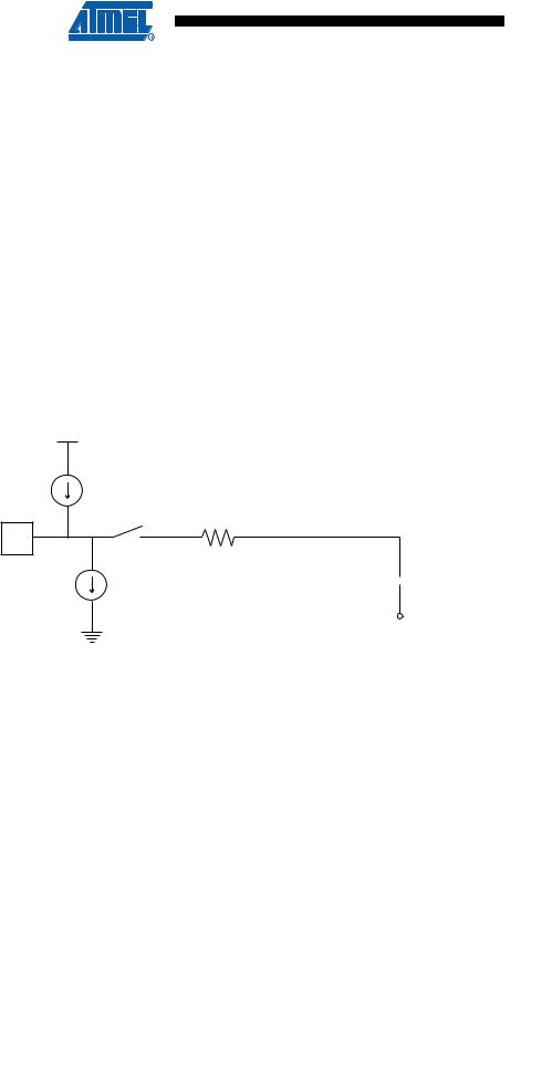
23.6.1Analog Input Circuitry
The analog input circuitry for single ended channels is illustrated in Figure 23-8. An analog source applied to ADCn is subjected to the pin capacitance and input leakage of that pin, regardless of whether that channel is selected as input for the ADC. When the channel is selected, the source must drive the S/H capacitor through the series resistance (combined resistance in the input path).
The ADC is optimized for analog signals with an output impedance of approximately 10 kΩ or less. If such a source is used, the sampling time will be negligible. If a source with higher impedance is used, the sampling time will depend on how long time the source needs to charge the S/H capacitor, with can vary widely. The user is recommended to only use low impedance sources with slowly varying signals, since this minimizes the required charge transfer to the S/H capacitor.
Signal components higher than the Nyquist frequency (fADC/2) should not be present for either kind of channels, to avoid distortion from unpredictable signal convolution. The user is advised to remove high frequency components with a low-pass filter before applying the signals as inputs to the ADC.
Figure 23-8. Analog Input Circuitry
IIH
ADCn
1..100 kOhm
CS/H= 14 pF 
IIL
VCC/2
23.6.2Analog Noise Canceling Techniques
Digital circuitry inside and outside the device generates EMI which might affect the accuracy of analog measurements. If conversion accuracy is critical, the noise level can be reduced by applying the following techniques:
a.Keep analog signal paths as short as possible. Make sure analog tracks run over the analog ground plane, and keep them well away from high-speed switching digital tracks.
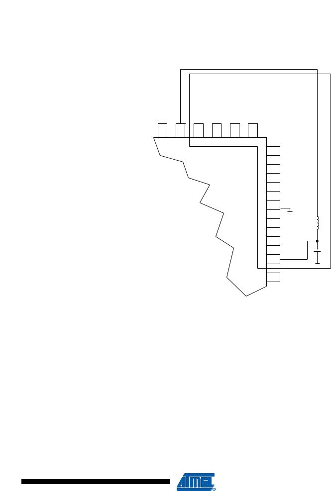
b.The AVCC pin on the device should be connected to the digital VCC supply voltage via an LC network as shown in Figure 23-9.
c.Use the ADC noise canceler function to reduce induced noise from the CPU.
d.If any ADC [3..0] port pins are used as digital outputs, it is essential that these do not switch while a conversion is in progress. However, using the 2-wire Interface (ADC4
252 ATmega48/88/168 
2545M–AVR–09/07
 ATmega48/88/168
and ADC5) will only affect the conversion on ADC4 and ADC5 and not the other ADC channels.
Figure 23-9. ADC Power Connections
GND |
VCC |
PC5(ADC5/SCL) |
PC4(ADC4/SDA) |
PC3(ADC3) |
PC2(ADC2) |
Analog Ground Plane
PC1 (ADC1)
PC0 (ADC0)
ADC7
GND |
|
|
AREF |
μH |
|
10 |
||
|
||
ADC6 |
100nF |
|
AVCC |
||
|
PB5
23.6.3ADC Accuracy Definitions
An n-bit single-ended ADC converts a voltage linearly between GND and VREF in 2n steps (LSBs). The lowest code is read as 0, and the highest code is read as 2n-1.
Several parameters describe the deviation from the ideal behavior:
•Offset: The deviation of the first transition (0x000 to 0x001) compared to the ideal transition (at 0.5 LSB). Ideal value: 0 LSB.
253
2545M–AVR–09/07
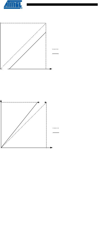
Figure 23-10. Offset Error
Output Code
Ideal ADC
Actual ADC
Offset
 Error
Error
VREF Input Voltage
•Gain error: After adjusting for offset, the gain error is found as the deviation of the last transition (0x3FE to 0x3FF) compared to the ideal transition (at 1.5 LSB below maximum). Ideal value: 0 LSB
Figure 23-11. Gain Error
Output Code |
Gain |
|
|
Error |
|
|
|
Ideal ADC |
|
|
Actual ADC |
|
VREF |
Input Voltage |
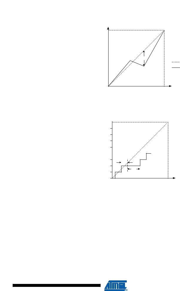
•Integral Non-linearity (INL): After adjusting for offset and gain error, the INL is the maximum deviation of an actual transition compared to an ideal transition for any code. Ideal value: 0 LSB.
254 ATmega48/88/168 
2545M–AVR–09/07
 ATmega48/88/168
Figure 23-12. Integral Non-linearity (INL) |
|
Output Code |
|
INL |
Ideal ADC |
|
|
|
Actual ADC |
VREF |
Input Voltage |
•Differential Non-linearity (DNL): The maximum deviation of the actual code width (the interval between two adjacent transitions) from the ideal code width (1 LSB). Ideal value: 0 LSB.
Figure 23-13. Differential Non-linearity (DNL)
Output Code
0x3FF
|
1 LSB |
|
DNL |
0x000 |
|
0 |
VREF Input Voltage |
•Quantization Error: Due to the quantization of the input voltage into a finite number of codes, a range of input voltages (1 LSB wide) will code to the same value. Always ±0.5 LSB.
•Absolute accuracy: The maximum deviation of an actual (unadjusted) transition compared to an ideal transition for any code. This is the compound effect of offset, gain error, differential error, non-linearity, and quantization error. Ideal value: ±0.5 LSB.
255
2545M–AVR–09/07