

- •Features
- •1. Pin Configurations
- •1.1 Pin Descriptions
- •1.1.3 Port B (PB7:0) XTAL1/XTAL2/TOSC1/TOSC2
- •1.1.4 Port C (PC5:0)
- •1.1.5 PC6/RESET
- •1.1.6 Port D (PD7:0)
- •1.1.8 AREF
- •1.1.9 ADC7:6 (TQFP and QFN/MLF Package Only)
- •2. Overview
- •2.1 Block Diagram
- •2.2 Comparison Between ATmega48, ATmega88, and ATmega168
- •3. Resources
- •4. Data Retention
- •5. About Code Examples
- •6. AVR CPU Core
- •6.1 Overview
- •6.2 Architectural Overview
- •6.4 Status Register
- •6.5 General Purpose Register File
- •6.6 Stack Pointer
- •6.7 Instruction Execution Timing
- •6.8 Reset and Interrupt Handling
- •6.8.1 Interrupt Response Time
- •7. AVR Memories
- •7.1 Overview
- •7.3 SRAM Data Memory
- •7.3.1 Data Memory Access Times
- •7.4 EEPROM Data Memory
- •7.4.1 EEPROM Read/Write Access
- •7.4.2 Preventing EEPROM Corruption
- •7.5 I/O Memory
- •7.5.1 General Purpose I/O Registers
- •7.6 Register Description
- •8. System Clock and Clock Options
- •8.1 Clock Systems and their Distribution
- •8.2 Clock Sources
- •8.2.1 Default Clock Source
- •8.2.2 Clock Startup Sequence
- •8.3 Low Power Crystal Oscillator
- •8.4 Full Swing Crystal Oscillator
- •8.5 Low Frequency Crystal Oscillator
- •8.6 Calibrated Internal RC Oscillator
- •8.7 128 kHz Internal Oscillator
- •8.8 External Clock
- •8.9 Clock Output Buffer
- •8.10 Timer/Counter Oscillator
- •8.11 System Clock Prescaler
- •8.12 Register Description
- •9. Power Management and Sleep Modes
- •9.1 Sleep Modes
- •9.2 Idle Mode
- •9.3 ADC Noise Reduction Mode
- •9.4 Power-down Mode
- •9.5 Power-save Mode
- •9.6 Standby Mode
- •9.7 Power Reduction Register
- •9.8 Minimizing Power Consumption
- •9.8.1 Analog to Digital Converter
- •9.8.2 Analog Comparator
- •9.8.4 Internal Voltage Reference
- •9.8.5 Watchdog Timer
- •9.8.6 Port Pins
- •9.9 Register Description
- •10. System Control and Reset
- •10.1 Resetting the AVR
- •10.2 Reset Sources
- •10.3 Power-on Reset
- •10.4 External Reset
- •10.6 Watchdog System Reset
- •10.7 Internal Voltage Reference
- •10.8 Watchdog Timer
- •10.8.1 Features
- •10.9 Register Description
- •11. Interrupts
- •11.1 Overview
- •11.2 Interrupt Vectors in ATmega48
- •11.3 Interrupt Vectors in ATmega88
- •11.4 Interrupt Vectors in ATmega168
- •11.4.1 Moving Interrupts Between Application and Boot Space, ATmega88 and ATmega168
- •11.5 Register Description
- •12. External Interrupts
- •12.1 Pin Change Interrupt Timing
- •12.2 Register Description
- •13. I/O-Ports
- •13.1 Overview
- •13.2 Ports as General Digital I/O
- •13.2.1 Configuring the Pin
- •13.2.2 Toggling the Pin
- •13.2.3 Switching Between Input and Output
- •13.2.4 Reading the Pin Value
- •13.2.5 Digital Input Enable and Sleep Modes
- •13.2.6 Unconnected Pins
- •13.3 Alternate Port Functions
- •13.3.1 Alternate Functions of Port B
- •13.3.2 Alternate Functions of Port C
- •13.3.3 Alternate Functions of Port D
- •13.4 Register Description
- •14. 8-bit Timer/Counter0 with PWM
- •14.1 Features
- •14.2 Overview
- •14.2.1 Definitions
- •14.2.2 Registers
- •14.3 Timer/Counter Clock Sources
- •14.4 Counter Unit
- •14.5 Output Compare Unit
- •14.5.1 Force Output Compare
- •14.5.2 Compare Match Blocking by TCNT0 Write
- •14.5.3 Using the Output Compare Unit
- •14.6 Compare Match Output Unit
- •14.6.1 Compare Output Mode and Waveform Generation
- •14.7 Modes of Operation
- •14.7.1 Normal Mode
- •14.7.2 Clear Timer on Compare Match (CTC) Mode
- •14.7.3 Fast PWM Mode
- •14.7.4 Phase Correct PWM Mode
- •14.8 Timer/Counter Timing Diagrams
- •14.9 Register Description
- •15. 16-bit Timer/Counter1 with PWM
- •15.1 Features
- •15.2 Overview
- •15.2.1 Registers
- •15.2.2 Definitions
- •15.3.1 Reusing the Temporary High Byte Register
- •15.4 Timer/Counter Clock Sources
- •15.5 Counter Unit
- •15.6 Input Capture Unit
- •15.6.1 Input Capture Trigger Source
- •15.6.2 Noise Canceler
- •15.6.3 Using the Input Capture Unit
- •15.7 Output Compare Units
- •15.7.1 Force Output Compare
- •15.7.2 Compare Match Blocking by TCNT1 Write
- •15.7.3 Using the Output Compare Unit
- •15.8 Compare Match Output Unit
- •15.8.1 Compare Output Mode and Waveform Generation
- •15.9 Modes of Operation
- •15.9.1 Normal Mode
- •15.9.2 Clear Timer on Compare Match (CTC) Mode
- •15.9.3 Fast PWM Mode
- •15.9.4 Phase Correct PWM Mode
- •15.9.5 Phase and Frequency Correct PWM Mode
- •15.10 Timer/Counter Timing Diagrams
- •15.11 Register Description
- •16. Timer/Counter0 and Timer/Counter1 Prescalers
- •16.0.1 Internal Clock Source
- •16.0.2 Prescaler Reset
- •16.0.3 External Clock Source
- •16.1 Register Description
- •17. 8-bit Timer/Counter2 with PWM and Asynchronous Operation
- •17.1 Features
- •17.2 Overview
- •17.2.1 Registers
- •17.2.2 Definitions
- •17.3 Timer/Counter Clock Sources
- •17.4 Counter Unit
- •17.5 Output Compare Unit
- •17.5.1 Force Output Compare
- •17.5.2 Compare Match Blocking by TCNT2 Write
- •17.5.3 Using the Output Compare Unit
- •17.6 Compare Match Output Unit
- •17.6.1 Compare Output Mode and Waveform Generation
- •17.7 Modes of Operation
- •17.7.1 Normal Mode
- •17.7.2 Clear Timer on Compare Match (CTC) Mode
- •17.7.3 Fast PWM Mode
- •17.7.4 Phase Correct PWM Mode
- •17.8 Timer/Counter Timing Diagrams
- •17.9 Asynchronous Operation of Timer/Counter2
- •17.10 Timer/Counter Prescaler
- •17.11 Register Description
- •18.1 Features
- •18.2 Overview
- •18.3 SS Pin Functionality
- •18.3.1 Slave Mode
- •18.3.2 Master Mode
- •18.4 Data Modes
- •18.5 Register Description
- •19. USART0
- •19.1 Features
- •19.2 Overview
- •19.3 Clock Generation
- •19.3.2 Double Speed Operation (U2Xn)
- •19.3.3 External Clock
- •19.3.4 Synchronous Clock Operation
- •19.4 Frame Formats
- •19.4.1 Parity Bit Calculation
- •19.5 USART Initialization
- •19.6.1 Sending Frames with 5 to 8 Data Bit
- •19.6.2 Sending Frames with 9 Data Bit
- •19.6.3 Transmitter Flags and Interrupts
- •19.6.4 Parity Generator
- •19.6.5 Disabling the Transmitter
- •19.7.1 Receiving Frames with 5 to 8 Data Bits
- •19.7.2 Receiving Frames with 9 Data Bits
- •19.7.3 Receive Compete Flag and Interrupt
- •19.7.4 Receiver Error Flags
- •19.7.5 Parity Checker
- •19.7.6 Disabling the Receiver
- •19.7.7 Flushing the Receive Buffer
- •19.8 Asynchronous Data Reception
- •19.8.1 Asynchronous Clock Recovery
- •19.8.2 Asynchronous Data Recovery
- •19.8.3 Asynchronous Operational Range
- •19.9.1 Using MPCMn
- •19.10 Register Description
- •19.11 Examples of Baud Rate Setting
- •20. USART in SPI Mode
- •20.1 Features
- •20.2 Overview
- •20.3 Clock Generation
- •20.4 SPI Data Modes and Timing
- •20.5 Frame Formats
- •20.5.1 USART MSPIM Initialization
- •20.6 Data Transfer
- •20.6.1 Transmitter and Receiver Flags and Interrupts
- •20.6.2 Disabling the Transmitter or Receiver
- •20.7 AVR USART MSPIM vs. AVR SPI
- •20.8 Register Description
- •20.8.5 USART MSPIM Baud Rate Registers - UBRRnL and UBRRnH
- •21. 2-wire Serial Interface
- •21.1 Features
- •21.2.1 TWI Terminology
- •21.2.2 Electrical Interconnection
- •21.3 Data Transfer and Frame Format
- •21.3.1 Transferring Bits
- •21.3.2 START and STOP Conditions
- •21.3.3 Address Packet Format
- •21.3.4 Data Packet Format
- •21.3.5 Combining Address and Data Packets into a Transmission
- •21.5 Overview of the TWI Module
- •21.5.1 SCL and SDA Pins
- •21.5.2 Bit Rate Generator Unit
- •21.5.3 Bus Interface Unit
- •21.5.4 Address Match Unit
- •21.5.5 Control Unit
- •21.6 Using the TWI
- •21.7 Transmission Modes
- •21.7.1 Master Transmitter Mode
- •21.7.2 Master Receiver Mode
- •21.7.3 Slave Receiver Mode
- •21.7.4 Slave Transmitter Mode
- •21.7.5 Miscellaneous States
- •21.7.6 Combining Several TWI Modes
- •21.9 Register Description
- •22. Analog Comparator
- •22.1 Overview
- •22.2 Analog Comparator Multiplexed Input
- •22.3 Register Description
- •23. Analog-to-Digital Converter
- •23.1 Features
- •23.2 Overview
- •23.3 Starting a Conversion
- •23.4 Prescaling and Conversion Timing
- •23.5 Changing Channel or Reference Selection
- •23.5.1 ADC Input Channels
- •23.5.2 ADC Voltage Reference
- •23.6 ADC Noise Canceler
- •23.6.1 Analog Input Circuitry
- •23.6.2 Analog Noise Canceling Techniques
- •23.6.3 ADC Accuracy Definitions
- •23.7 ADC Conversion Result
- •23.8 Register Description
- •23.8.3.1 ADLAR = 0
- •23.8.3.2 ADLAR = 1
- •24. debugWIRE On-chip Debug System
- •24.1 Features
- •24.2 Overview
- •24.3 Physical Interface
- •24.4 Software Break Points
- •24.5 Limitations of debugWIRE
- •24.6 Register Description
- •25. Self-Programming the Flash, ATmega48
- •25.1 Overview
- •25.1.1 Performing Page Erase by SPM
- •25.1.2 Filling the Temporary Buffer (Page Loading)
- •25.1.3 Performing a Page Write
- •25.2.1 EEPROM Write Prevents Writing to SPMCSR
- •25.2.2 Reading the Fuse and Lock Bits from Software
- •25.2.3 Preventing Flash Corruption
- •25.2.4 Programming Time for Flash when Using SPM
- •25.2.5 Simple Assembly Code Example for a Boot Loader
- •25.3 Register Description
- •26.1 Features
- •26.2 Overview
- •26.3 Application and Boot Loader Flash Sections
- •26.3.1 Application Section
- •26.5 Boot Loader Lock Bits
- •26.6 Entering the Boot Loader Program
- •26.8.1 Performing Page Erase by SPM
- •26.8.2 Filling the Temporary Buffer (Page Loading)
- •26.8.3 Performing a Page Write
- •26.8.4 Using the SPM Interrupt
- •26.8.5 Consideration While Updating BLS
- •26.8.7 Setting the Boot Loader Lock Bits by SPM
- •26.8.8 EEPROM Write Prevents Writing to SPMCSR
- •26.8.9 Reading the Fuse and Lock Bits from Software
- •26.8.10 Preventing Flash Corruption
- •26.8.11 Programming Time for Flash when Using SPM
- •26.8.12 Simple Assembly Code Example for a Boot Loader
- •26.8.13 ATmega88 Boot Loader Parameters
- •26.8.14 ATmega168 Boot Loader Parameters
- •26.9 Register Description
- •27. Memory Programming
- •27.1 Program And Data Memory Lock Bits
- •27.2 Fuse Bits
- •27.2.1 Latching of Fuses
- •27.3 Signature Bytes
- •27.4 Calibration Byte
- •27.5 Page Size
- •27.6 Parallel Programming Parameters, Pin Mapping, and Commands
- •27.6.1 Signal Names
- •27.7 Parallel Programming
- •27.7.1 Enter Programming Mode
- •27.7.2 Considerations for Efficient Programming
- •27.7.3 Chip Erase
- •27.7.4 Programming the Flash
- •27.7.5 Programming the EEPROM
- •27.7.6 Reading the Flash
- •27.7.7 Reading the EEPROM
- •27.7.8 Programming the Fuse Low Bits
- •27.7.9 Programming the Fuse High Bits
- •27.7.10 Programming the Extended Fuse Bits
- •27.7.11 Programming the Lock Bits
- •27.7.12 Reading the Fuse and Lock Bits
- •27.7.13 Reading the Signature Bytes
- •27.7.14 Reading the Calibration Byte
- •27.7.15 Parallel Programming Characteristics
- •27.8 Serial Downloading
- •27.8.1 Serial Programming Pin Mapping
- •27.8.2 Serial Programming Algorithm
- •27.8.3 Serial Programming Instruction set
- •27.8.4 SPI Serial Programming Characteristics
- •28. Electrical Characteristics
- •28.1 Absolute Maximum Ratings*
- •28.2 DC Characteristics
- •28.3 Speed Grades
- •28.4 Clock Characteristics
- •28.4.1 Calibrated Internal RC Oscillator Accuracy
- •28.4.2 External Clock Drive Waveforms
- •28.4.3 External Clock Drive
- •28.5 System and Reset Characteristics
- •28.7 SPI Timing Characteristics
- •28.8 ADC Characteristics
- •28.9 Parallel Programming Characteristics
- •29. Typical Characteristics
- •29.1 Active Supply Current
- •29.2 Idle Supply Current
- •29.3 Supply Current of I/O modules
- •29.3.0.1 Example 1
- •29.3.0.2 Example 2
- •29.3.0.3 Example 3
- •29.6 Standby Supply Current
- •29.8 Pin Driver Strength
- •29.9 Pin Thresholds and Hysteresis
- •29.10 BOD Thresholds and Analog Comparator Offset
- •29.11 Internal Oscillator Speed
- •29.12 Current Consumption of Peripheral Units
- •29.13 Current Consumption in Reset and Reset Pulse width
- •30. Register Summary
- •31. Instruction Set Summary
- •32. Ordering Information
- •32.1 ATmega48
- •32.2 ATmega88
- •32.3 ATmega168
- •33. Packaging Information
- •34. Errata
- •34.1 Errata ATmega48
- •34.2 Errata ATmega88
- •34.3 Errata ATmega168
- •35. Datasheet Revision History
 ATmega48/88/168
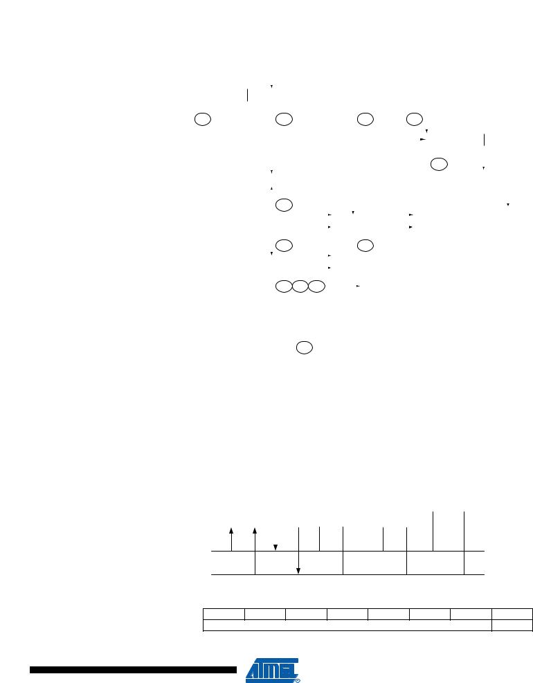
Figure 21-14. Formats and States in the Master Receiver Mode
MR
Successfull |
|
|
|
|
|
|
|
|
|
|
|
|
|
|
|
|
|
|
|
|
|
|
|
|
|
|
|
|
|
|
|
|
|
|
|
|
|
|
|
|
|
|
|
|
|
|
|
|
|
|
|
|
|
|
|
|
|
|
|
|
|
|
|
|
|
|
|
|
|
|
|
|
|
|
|
||
|
|
|
|
|
|
|
|
|
|
|
|
|
|
|
|
|
|
|
|
|
|
|
|
|
|
|
|
|
|
|
|
|
|
|
|
|
||
|
S |
SLA |
R |
|
A |
|
|
|
DATA |
|
|
|
A |
DATA |
|
|
|
|
|
|
|
P |
|
|
|
|
||||||||||||
reception |
|
|
|
|
|
|
|
|
|
|
|
A |
|
|
|
|
|
|||||||||||||||||||||
from a slave |
|
|
|
|
|
|
|
|
|
|
|
|
|
|
|
|
|
|
|
|
|
|
|
|
|
|
|
|
|
|
|
|
|
|
|
|
|
|
receiver |
|
|
|
|
|
|
|
|
|
|
|
|
|
|
|
|
|
|
|
|
|
|
|
|
|
|
|
|
|
|
|
|
|
|
|
|
||
|
|
|
|
|
|
|
|
|
|
|
|
|
|
|
|
|
|
|
|
|
|
|
|
|
|
|
|
|
|
|
|
|
|
|
|
|
|
|
|
|
|
$08 |
|
|
$40 |
|
|
|
|
|
|
|
|
$50 |
|
|
$58 |
|
|
|
|
|
|
|
|||||||||||||
Next transfer |
|
|
|
|
|
|
|
|
|
|
|
|
|
|
|
|
|
|
|
|
|
|
|
|
|
|
|
|
|
|
|
|
|
|
|
|
||
|
|
|
|
|
|
|
|
|
|
|
|
|
|
|
|
|
|
|
|
|
|
|
|
|
|
|
|
|
|
|
|
|
|
|
|
|||
|
|
|
|
|
|
|
|
|
|
|
|
|
|
|
|
|
|
|
|
|
|
|
|
|
|
|
|
|
|
RS |
SLA |
R |
|
|||||
started with a |
|
|
|
|
|
|
|
|
|
|
|
|
|
|
|
|
|
|
|
|
|
|
|
|
|
|
|
|
|
|
|
|||||||
repeated start |
|
|
|
|
|
|
|
|
|
|
|
|
|
|
|
|
|
|
|
|
|
|
|
|
|
|
|
|
|
|
|
|
|
|
|
|
||
condition |
|
|
|
|
|
|
|
|
|
|
|
|
|
|
|
|
|
|
|
|
|
|
|
|
|
|
|
|
|
|
|
|
|
|
|
|
||
|
|
|
|
|
|
|
|
|
|
|
|
|
|
|
|
|
|
|
|
|
|
|
|
|
|
|
|
|
|
|
|
|
|
|
|
|
|
|
|
|
|
|
|
|
|
|
|
|
|
|
|
|
|
|
|
|
|
|
|
|
|
|
|
|
|
|
|
|
|
|
|
$10 |
|
|
|
|
|
|
|
|
|
|
|
|
|
|
|
|
|
|
|
|
|
|
|
|
|
|
|
|
|
|
|
|
|
|
|
|
|
|
|
|
|
|
|
|
Not acknowledge |
|
|
|
|
|
|
|
|
|
|
|
|
|
|
|
|
|
|
|
|
|
|
|
|
|
|
|
|
|
|
|
|
W |
|
||||
|
|
|
|
|
|
|
|
|
P |
|
|
|
|
|
|
|
|
|
|
|
|
|
|
|
|
|
|
|
|
|
||||||||
received after the |
|
|
|
A |
|
|
|
|
|
|
|
|
|
|
|
|
|
|
|
|
|
|
|
|
|
|
|
|
|
|
|
|||||||
|
|
|
|
|
|
|
|
|
|
|
|
|
|
|
|
|
|
|
|
|
|
|
|
|
|
|
|
|
|
|||||||||
slave address |
|
|
|
|
|
|
|
|
|
|
|
|
|
|
|
|
|
|
|
|
|
|
|
|
|
|
|
|
|
|
|
|
|
|
|
|
||
|
|
|
|
|
|
|
|
|
|
|
|
|
|
|
|
|
|
|
|
|
|
|
|
|
|
|
|
|
|
|
|
|
|
|
|
|
|
|
|
|
|
|
|
|
|
$48 |
|
|
|
|
|
|
|
|
|
|
|
|
|
|
|
|
|
|
|
|
|
|
|
|
|
|
|
||||
Arbitration lost in slave |
|
|
|
|
|
|
|
|
|
|
|
|
|
|
|
|
|
|
|
|
|
|
|
|
|
|
|
MT |
||||||||||
|
|
|
|
|
|
|
|
|
|
|
|
|
|
|
|
|
|
|
|
|
|
|
|
|
|
|
|
|
|
|
|
|||||||
|
|
|
|
|
|
|
|
|
|
|
|
|
|
|
|
|
|
|
|
|
|
|
|
|
|
|
|
|
|
|
|
|||||||
|
|
|
|
|
|
|
|
Other master |
|
|
|
|
|
|
Other master |
|
|
|
|
|
|
|
|
|
|
|
|
|||||||||||
address or data byte |
|
|
A or A |
|
continues |
|
|
|
|
A |
continues |
|
|
|
|
|
|
|
|
|
|
|
|
|||||||||||||||
|
|
|
|
|
|
|
|
|
|
|
|
|
|
|
|
|
|
|
|
|
|
|
|
|
|
|
|
|
|
|
|
|
|
|
|
|
||
|
|
|
|
|
|
|
$38 |
|
|
|
|
|
|
|
$38 |
|
|
|
|
|
|
|
|
|
|
|
|
|
|
|||||||||
Arbitration lost and |
|
|
|
|
|
|
|
|
|
|
|
|
|
|
|
|
|
|
|
|
|
|
|
|
|
|
|
|
|
|
|
|
||||||
|
|
|
|
|
|
|
|
|
|
|
|
|
|
|
|
|
|
|
|
|
|
|
|
|
|
|
|
|
|
|
|
|||||||
|
|
|
A |
|
Other master |
|
|
|
|
|
|
|
|
|
|
|
|
|
|
|
|
|
|
|
|
|||||||||||||
addressed as slave |
|
|
|
|
continues |
|
|
|
|
|
|
|
|
|
|
|
|
|
|
|
|
|
|
|
|
|||||||||||||
|
|
|
|
|
|
|
|
|
|
|
|
|
|
|
|
|
|
|
|
|
To corresponding |
|
|
|
|
|
|
|
|
|
|
|
|
|||||
|
|
|
|
|
|
|
|
|
|
|
|
|
|
|
|
|
|
|
|
|
|
|
|
|
|
|
|
|
|
|
|
|
||||||
|
|
|
|
|
|
|
$68 |
$78 |
$B0 |
|
|
|
|
|
|
|
|
|
|
|
|
|
|
|
|
|||||||||||||
|
|
|
|
|
|
|
|
|
|
states in slave mode |
|
|
|
|
|
|
|
|
|
|
|
|
||||||||||||||||
|
|
|
|
|
|
|
|
|
|
|
|
|
|
|
|
|
|
|
|
|
|
|
|
|
|
|
|
|
|
|
|
|
|
|||||
|
|
|
|
|
|
|
|
|
|
|
|
|
|
|
|
|
|
|
Any number of data bytes |
|
|
|
|
|
|
|
|
|
|
|
|
|||||||
|
|
|
From master to slave |
|
DATA |
|
|
|
|
A |
|
|
|
|
|
|
|
|
|
|
|
|
||||||||||||||||
|
|
|
|
|
|
|
|
and their associated acknowledge bits |
|
|
|
|
|
|
||||||||||||||||||||||||
|
|
|
From slave to master |
|
|
|
|
|
|
|
n |
|
|
|
|
|
This number (contained in TWSR) corresponds |
|
|
|
|
|||||||||||||||||
|
|
|
|
|
|
|
|
|
|
|
|
|
|
|
|
|
|
|
||||||||||||||||||||
|
|
|
|
|
|
|
|
|
|
|
|
|
|
|
|
|
|
to a defined state of the 2-Wire Serial Bus. The |
|
|
|
|
||||||||||||||||
|
|
|
|
|
|
|
|
|
|
|
|
|
|
|
|
|
|
|
|
|
|
|||||||||||||||||
prescaler bits are zero or masked to zero
21.7.3Slave Receiver Mode
In the Slave Receiver mode, a number of data bytes are received from a Master Transmitter (see Figure 21-15). All the status codes mentioned in this section assume that the prescaler bits are zero or are masked to zero.
Figure 21-15. Data transfer in Slave Receiver mode
|
|
|
|
|
|
|
VCC |
|
|
|
|
|
|
|
|
|
|
|
|
|
|
|
|
|
|
|
|
|
|
|
|
|
|
|
|
|
|
|
|
|
|
|
|
|
|
|
|
Device 1 |
|
Device 2 |
|
Device 3 |
........ |
|
|
|
|
|
|
|
|
|
|
|
|
Device n |
|
|
R1 |
|
R2 |
|
|||||||
SLAVE |
|
|
MASTER |
|
|
|
|
|
|||||||
RECEIVER |
|
TRANSMITTER |
|
|
|
|
|
|
|
|
|
|
|
|
|
|
|
|
|
|
|
|
|
|
|
|
|
|
|
|
|
|
|
|
|
|
|
|
|
|
|
|
|
|
|
|
|
|
|
|
|
|
|
|
|
|
|
|
|
|
|
|
|
SDA
SCL
To initiate the Slave Receiver mode, TWAR and TWCR must be initialized as follows:
TWAR |
TWA6 |
TWA5 |
TWA4 |
TWA3 |
TWA2 |
TWA1 |
TWA0 |
TWGCE |
value |
|
|
Device’s Own Slave Address |
|
|
|
||
229
2545M–AVR–09/07

The upper 7 bits are the address to which the 2-wire Serial Interface will respond when addressed by a Master. If the LSB is set, the TWI will respond to the general call address (0x00), otherwise it will ignore the general call address.
TWCR |
TWINT |
TWEA |
TWSTA |
TWSTO |
TWWC |
TWEN |
– |
TWIE |
value |
0 |
1 |
0 |
0 |
0 |
1 |
0 |
X |
|
|
|
|
|
|
|
|
|
TWEN must be written to one to enable the TWI. The TWEA bit must be written to one to enable the acknowledgement of the device’s own slave address or the general call address. TWSTA and TWSTO must be written to zero.
When TWAR and TWCR have been initialized, the TWI waits until it is addressed by its own slave address (or the general call address if enabled) followed by the data direction bit. If the direction bit is “0” (write), the TWI will operate in SR mode, otherwise ST mode is entered. After its own slave address and the write bit have been received, the TWINT Flag is set and a valid status code can be read from TWSR. The status code is used to determine the appropriate software action. The appropriate action to be taken for each status code is detailed in Table 21-4. The Slave Receiver mode may also be entered if arbitration is lost while the TWI is in the Master mode (see states 0x68 and 0x78).
If the TWEA bit is reset during a transfer, the TWI will return a “Not Acknowledge” (“1”) to SDA after the next received data byte. This can be used to indicate that the Slave is not able to receive any more bytes. While TWEA is zero, the TWI does not acknowledge its own slave address. However, the 2-wire Serial Bus is still monitored and address recognition may resume at any time by setting TWEA. This implies that the TWEA bit may be used to temporarily isolate the TWI from the 2-wire Serial Bus.
In all sleep modes other than Idle mode, the clock system to the TWI is turned off. If the TWEA bit is set, the interface can still acknowledge its own slave address or the general call address by using the 2-wire Serial Bus clock as a clock source. The part will then wake up from sleep and the TWI will hold the SCL clock low during the wake up and until the TWINT Flag is cleared (by writing it to one). Further data reception will be carried out as normal, with the AVR clocks running as normal. Observe that if the AVR is set up with a long start-up time, the SCL line may be held low for a long time, blocking other data transmissions.
Note that the 2-wire Serial Interface Data Register – TWDR does not reflect the last byte present on the bus when waking up from these Sleep modes.
230 ATmega48/88/168 
2545M–AVR–09/07
ATmega48/88/168
Table 21-4. |
Status Codes for Slave Receiver Mode |
|
|
|
|
|
||
Status Code |
Status of the 2-wire Serial Bus |
Application Software Response |
|
|
||||
(TWSR) |
|
|
To TWCR |
|
|
|||
Prescaler Bits |
and 2-wire Serial Interface Hard- |
To/from TWDR |
|
|
|
|||
are 0 |
ware |
STA |
STO |
TWIN |
TWE |
Next Action Taken by TWI Hardware |
||
|
||||||||
|
|
|
|
|
T |
A |
|
|
0x60 |
Own SLA+W has been received; |
No TWDR action or |
X |
0 |
1 |
0 |
Data byte will be received and NOT ACK will be |
|
|
ACK has been returned |
No TWDR action |
X |
0 |
1 |
1 |
returned |
|
|
|
Data byte will be received and ACK will be returned |
||||||
0x68 |
Arbitration lost in SLA+R/W as |
No TWDR action or |
X |
0 |
1 |
0 |
Data byte will be received and NOT ACK will be |
|
|
Master; own SLA+W has been |
|
|
|
|
|
returned |
|
|
received; ACK has been returned |
No TWDR action |
X |
0 |
1 |
1 |
Data byte will be received and ACK will be returned |
|
0x70 |
General call address has been |
No TWDR action or |
X |
0 |
1 |
0 |
Data byte will be received and NOT ACK will be |
|
|
received; ACK has been returned |
|
|
|
|
|
returned |
|
|
|
No TWDR action |
X |
0 |
1 |
1 |
Data byte will be received and ACK will be returned |
|
0x78 |
Arbitration lost in SLA+R/W as |
No TWDR action or |
X |
0 |
1 |
0 |
Data byte will be received and NOT ACK will be |
|
|
Master; General call address has |
|
|
|
|
|
returned |
|
|
been received; ACK has been |
No TWDR action |
X |
0 |
1 |
1 |
Data byte will be received and ACK will be returned |
|
|
returned |
|
|
|
|
|
|
|
0x80 |
Previously addressed with own |
Read data byte or |
X |
0 |
1 |
0 |
Data byte will be received and NOT ACK will be |
|
|
SLA+W; data has been received; |
|
|
|
|
|
returned |
|
|
ACK has been returned |
Read data byte |
X |
0 |
1 |
1 |
Data byte will be received and ACK will be returned |
|
0x88 |
Previously addressed with own |
Read data byte or |
0 |
0 |
1 |
0 |
Switched to the not addressed Slave mode; |
|
|
SLA+W; data has been received; |
|
|
|
|
|
no recognition of own SLA or GCA |
|
|
NOT ACK has been returned |
Read data byte or |
0 |
0 |
1 |
1 |
Switched to the not addressed Slave mode; |
|
|
|
|
|
|
|
|
own SLA will be recognized; |
|
|
|
Read data byte or |
1 |
0 |
1 |
0 |
GCA will be recognized if TWGCE = “1” |
|
|
|
Switched to the not addressed Slave mode; |
||||||
|
|
|
|
|
|
|
no recognition of own SLA or GCA; |
|
|
|
|
|
|
|
|
a START condition will be transmitted when the bus |
|
|
|
Read data byte |
1 |
0 |
1 |
1 |
becomes free |
|
|
|
Switched to the not addressed Slave mode; |
||||||
|
|
|
|
|
|
|
own SLA will be recognized; |
|
|
|
|
|
|
|
|
GCA will be recognized if TWGCE = “1”; |
|
|
|
|
|
|
|
|
a START condition will be transmitted when the bus |
|
|
|
|
|
|
|
|
becomes free |
|
0x90 |
Previously addressed with |
Read data byte or |
X |
0 |
1 |
0 |
Data byte will be received and NOT ACK will be |
|
|
general call; data has been re- |
|
|
|
|
|
returned |
|
|
ceived; ACK has been returned |
Read data byte |
X |
0 |
1 |
1 |
Data byte will be received and ACK will be returned |
|
0x98 |
Previously addressed with |
Read data byte or |
0 |
0 |
1 |
0 |
Switched to the not addressed Slave mode; |
|
|
general call; data has been |
|
|
|
|
|
no recognition of own SLA or GCA |
|
|
received; NOT ACK has been |
Read data byte or |
0 |
0 |
1 |
1 |
Switched to the not addressed Slave mode; |
|
|
returned |
|
|
|
|
|
own SLA will be recognized; |
|
|
|
Read data byte or |
1 |
0 |
1 |
0 |
GCA will be recognized if TWGCE = “1” |
|
|
|
Switched to the not addressed Slave mode; |
||||||
|
|
|
|
|
|
|
no recognition of own SLA or GCA; |
|
|
|
|
|
|
|
|
a START condition will be transmitted when the bus |
|
|
|
Read data byte |
1 |
0 |
1 |
1 |
becomes free |
|
|
|
Switched to the not addressed Slave mode; |
||||||
|
|
|
|
|
|
|
own SLA will be recognized; |
|
|
|
|
|
|
|
|
GCA will be recognized if TWGCE = “1”; |
|
|
|
|
|
|
|
|
a START condition will be transmitted when the bus |
|
|
|
|
|
|
|
|
becomes free |
|
0xA0 |
A STOP condition or repeated |
No action |
0 |
0 |
1 |
0 |
Switched to the not addressed Slave mode; |
|
|
START condition has been |
|
|
|
|
|
no recognition of own SLA or GCA |
|
|
received while still addressed as |
|
0 |
0 |
1 |
1 |
Switched to the not addressed Slave mode; |
|
|
Slave |
|
|
|
|
|
own SLA will be recognized; |
|
|
|
|
|
|
|
|
GCA will be recognized if TWGCE = “1” |
|
|
|
|
1 |
0 |
1 |
0 |
Switched to the not addressed Slave mode; |
|
|
|
|
|
|
|
|
no recognition of own SLA or GCA; |
|
|
|
|
|
|
|
|
a START condition will be transmitted when the bus |
|
|
|
|
1 |
0 |
1 |
1 |
becomes free |
|
|
|
|
Switched to the not addressed Slave mode; |
|||||
|
|
|
|
|
|
|
own SLA will be recognized; |
|
|
|
|
|
|
|
|
GCA will be recognized if TWGCE = “1”; |
|
|
|
|
|
|
|
|
a START condition will be transmitted when the bus |
|
|
|
|
|
|
|
|
becomes free |
|
231
2545M–AVR–09/07
Figure 21-16. Formats and States in the Slave Receiver Mode
Reception of the own |
|
S |
SLA |
W |
|
A |
|
DATA |
A |
|
DATA |
|
|
A |
P or S |
|
|||||||
slave address and one or |
|
|
|
|
|
|
|
||||||||||||||||
more data bytes. All are |
|
|
|
|
|
|
|
|
|
|
|
|
|
|
|
|
|
|
|
|
|
|
|
acknowledged |
|
|
|
|
|
|
|
|
|
|
|
|
|
|
|
|
|
|
|
|
|
||
|
|
|
|
|
|
|
|
|
|
|
|
|
|
|
|
|
|
|
|
|
|
|
|
|
|
|
|
|
|
|
$60 |
|
|
|
$80 |
|
|
|
$80 |
$A0 |
|
||||||
Last data byte received |
|
|
|
|
|
|
|
|
|
|
|
|
|
|
|
|
|
|
|
|
|
||
|
|
|
|
|
|
|
|
|
|
|
|
|
|
|
|
|
|
|
|
|
|||
|
|
|
|
|
|
|
|
|
|
|
|
|
|
|
|
|
|
P or S |
|
||||
is not acknowledged |
|
|
|
|
|
|
|
|
|
|
|
|
|
|
|
A |
|
|
|||||
|
|
|
|
|
|
|
|
|
|
|
|
|
|
|
|
|
|
|
|
|
|
|
|
|
|
|
|
|
|
|
|
|
|
|
|
|
|
|
|
|
$88 |
|
|
|
|||
Arbitration lost as master |
|
|
|
|
|
|
|
|
|
|
|
|
|
|
|
|
|
|
|
|
|
||
|
|
|
|
|
|
|
|
|
|
|
|
|
|
|
|
|
|
|
|
|
|||
|
|
|
|
A |
|
|
|
|
|
|
|
|
|
|
|
|
|
|
|
||||
and addressed as slave |
|
|
|
|
|
|
|
|
|
|
|
|
|
|
|
|
|
|
|
||||
|
|
|
|
|
|
|
|
|
|
|
|
|
|
|
|
|
|
|
|
|
|
|
|
|
|
|
|
|
|
|
|
|
|
|
|
|
|
|
|
|
|
|
|
|
|
|
|
|
|
|
|
|
|
|
$68 |
|
|
|
|
|
|
|
|
|
|
|
|
|
|
|
|
Reception of the general call |
|
|
|
|
|
|
|
|
|
|
|
|
|
|
|
|
|
|
|
|
|
||
|
|
|
|
|
|
|
|
|
|
|
|
|
|
|
|
|
|
|
|
|
|||
|
General Call |
|
A |
|
DATA |
A |
|
DATA |
|
|
A |
P or S |
|
||||||||||
address and one or more data |
|
|
|
|
|
|
|
||||||||||||||||
bytes |
|
|
|
|
|
|
|
|
|
|
|
|
|
|
|
|
|
|
|
|
|
||
|
|
|
|
|
|
|
|
|
|
|
|
|
|
|
|
|
|
|
|
|
|
|
|
|
|
|
|
|
|
|
$70 |
|
|
|
$90 |
|
|
|
$90 |
$A0 |
|
||||||
Last data byte received is |
|
|
|
|
|
|
|
|
|
|
|
|
|
|
|
|
|
|
|
|
|
||
|
|
|
|
|
|
|
|
|
|
|
|
|
|
|
|
|
|
|
|
|
|||
|
|
|
|
|
|
|
|
|
|
|
|
|
|
|
|
|
|
P or S |
|
||||
not acknowledged |
|
|
|
|
|
|
|
|
|
|
|
|
|
|
|
A |
|
|
|||||
|
|
|
|
|
|
|
|
|
|
|
|
|
|
|
|
|
|
|
|
|
|
|
|
|
|
|
|
|
|
|
|
|
|
|
|
|
|
|
|
|
$98 |
|
|
|
|||
Arbitration lost as master and |
|
|
|
|
|
|
|
|
|
|
|
|
|
|
|
|
|
|
|
|
|
||
|
|
|
|
|
|
|
|
|
|
|
|
|
|
|
|
|
|
|
|
|
|||
|
|
|
|
A |
|
|
|
|
|
|
|
|
|
|
|
|
|
|
|
||||
addressed as slave by general call |
|
|
|
|
|
|
|
|
|
|
|
|
|
|
|
|
|
|
|||||
|
|
|
|
|
|
|
|
|
|
|
|
|
|
|
|
|
|
|
|
|
|
|
|
|
|
|
|
|
|
|
|
|
|
|
|
|
|
|
|
|
|
|
|
|
|
|
|
|
|
|
|
|
|
|
$78 |
|
|
|
|
|
|
|
|
|
|
|
|
|
|
|
|
|
|
|
|
|
|
|
|
|
|
|
|
|
|
|
|
|
|
|
|
|
|||
|
|
|
|
|
|
|
|
|
|
|
Any number of data bytes |
|
|
|
|
|
|
|
|
|
|||
|
From master to slave |
|
DATA |
|
|
A |
|
|
|
|
|
|
|
|
|
|
|||||||
|
|
|
|
|
and their associated acknowledge bits |
|
|
|
|
|
|
|
|||||||||||
|
From slave to master |
|
|
|
|
n |
|
|
This number (contained in TWSR) corresponds |
|
|
|
|||||||||||
|
|
|
|
|
|
|
|
|
|
||||||||||||||
|
|
|
|
|
|
|
|
|
|
to a defined state of the 2-Wire Serial Bus. The |
|
|
|
||||||||||
|
|
|
|
|
|
|
|
|
|
|
|
||||||||||||
prescaler bits are zero or masked to zero
21.7.4Slave Transmitter Mode
In the Slave Transmitter mode, a number of data bytes are transmitted to a Master Receiver (see Figure 21-17). All the status codes mentioned in this section assume that the prescaler bits are zero or are masked to zero.
Figure 21-17. Data Transfer in Slave Transmitter Mode
|
|
|
|
|
|
|
VCC |
|
|
|
|
|
|
|
|
|
|
|
|
|
|
|
|
|
|
|
|
|
|
|
|
|
|
|
|
|
|
|
|
|
|
|
|
|
|
|
|
Device 1 |
|
Device 2 |
|
Device 3 |
........ |
|
|
|
|
|
|
|
|
|
|
|
|
Device n |
|
|
R1 |
|
R2 |
|
|||||||
|
SLAVE |
|
MASTER |
|
|
|
|
|
|||||||
TRANSMITTER |
|
RECEIVER |
|
|
|
|
|
|
|
|
|
|
|
|
|
|
|
|
|
|
|
|
|
|
|
|
|
|
|
|
|
|
|
|
|
|
|
|
|
|
|
|
|
|
|
|
|
|
|
|
|
|
|
|
|
|
|
|
|
|
|
|
|
SDA
SCL
232 ATmega48/88/168
2545M–AVR–09/07

ATmega48/88/168
To initiate the Slave Transmitter mode, TWAR and TWCR must be initialized as follows:
TWAR |
TWA6 |
TWA5 |
TWA4 |
TWA3 |
TWA2 |
TWA1 |
TWA0 |
TWGCE |
value |
|
|
|
|
|
|
|
|
|
|
Device’s Own Slave Address |
|
|
|
|||
|
|
|
|
|
|
|
|
|
The upper seven bits are the address to which the 2-wire Serial Interface will respond when addressed by a Master. If the LSB is set, the TWI will respond to the general call address (0x00), otherwise it will ignore the general call address.
TWCR |
TWINT |
TWEA |
TWSTA |
TWSTO |
TWWC |
TWEN |
– |
TWIE |
value |
0 |
1 |
0 |
0 |
0 |
1 |
0 |
X |
|
|
|
|
|
|
|
|
|
TWEN must be written to one to enable the TWI. The TWEA bit must be written to one to enable the acknowledgement of the device’s own slave address or the general call address. TWSTA and TWSTO must be written to zero.
When TWAR and TWCR have been initialized, the TWI waits until it is addressed by its own slave address (or the general call address if enabled) followed by the data direction bit. If the direction bit is “1” (read), the TWI will operate in ST mode, otherwise SR mode is entered. After its own slave address and the write bit have been received, the TWINT Flag is set and a valid status code can be read from TWSR. The status code is used to determine the appropriate software action. The appropriate action to be taken for each status code is detailed in Table 21-5. The Slave Transmitter mode may also be entered if arbitration is lost while the TWI is in the Master mode (see state 0xB0).
If the TWEA bit is written to zero during a transfer, the TWI will transmit the last byte of the transfer. State 0xC0 or state 0xC8 will be entered, depending on whether the Master Receiver transmits a NACK or ACK after the final byte. The TWI is switched to the not addressed Slave mode, and will ignore the Master if it continues the transfer. Thus the Master Receiver receives all “1” as serial data. State 0xC8 is entered if the Master demands additional data bytes (by transmitting ACK), even though the Slave has transmitted the last byte (TWEA zero and expecting NACK from the Master).
While TWEA is zero, the TWI does not respond to its own slave address. However, the 2-wire Serial Bus is still monitored and address recognition may resume at any time by setting TWEA. This implies that the TWEA bit may be used to temporarily isolate the TWI from the 2-wire Serial Bus.
In all sleep modes other than Idle mode, the clock system to the TWI is turned off. If the TWEA bit is set, the interface can still acknowledge its own slave address or the general call address by using the 2-wire Serial Bus clock as a clock source. The part will then wake up from sleep and the TWI will hold the SCL clock will low during the wake up and until the TWINT Flag is cleared (by writing it to one). Further data transmission will be carried out as normal, with the AVR clocks running as normal. Observe that if the AVR is set up with a long start-up time, the SCL line may be held low for a long time, blocking other data transmissions.
Note that the 2-wire Serial Interface Data Register – TWDR does not reflect the last byte present on the bus when waking up from these sleep modes.
233
2545M–AVR–09/07

Table 21-5. |
Status Codes for Slave Transmitter Mode |
|
|
|
|
|
|
|
|
|
||
|
|
|
|
|
|
|
|
|
||||
|
|
|
|
|
|
|
|
|
||||
|
|
|
|
|
|
|
|
|
|
|
|
|
Status Code |
Status of the 2-wire Serial Bus |
Application Software Response |
|
|
|
|||||||
(TWSR) |
|
|
|
To TWCR |
|
|
|
|||||
Prescaler |
and 2-wire Serial Interface Hard- |
To/from TWDR |
|
|
|
|
|
|||||
Bits |
ware |
STA |
STO |
TWIN |
TWE |
Next Action Taken by TWI Hardware |
|
|||||
|
|
|||||||||||
are 0 |
|
|
|
|
|
|
|
T |
A |
|
|
|
0xA8 |
Own SLA+R has been received; |
Load data byte or |
X |
0 |
|
|
|
1 |
|
0 |
Last data byte will be transmitted and NOT ACK should |
|
|
ACK has been returned |
Load data byte |
X |
0 |
|
|
|
1 |
|
1 |
be received |
|
|
|
|
|
|
|
Data byte will be transmitted and ACK should be re- |
|
|||||
|
|
|
|
|
|
|
|
|
|
|
ceived |
|
0xB0 |
Arbitration lost in SLA+R/W as |
Load data byte or |
X |
0 |
|
|
|
1 |
|
0 |
Last data byte will be transmitted and NOT ACK should |
|
|
Master; own SLA+R has been |
|
|
|
|
|
|
|
|
|
be received |
|
|
received; ACK has been returned |
Load data byte |
X |
0 |
|
|
|
1 |
|
1 |
Data byte will be transmitted and ACK should be re- |
|
|
|
|
|
|
|
|
|
|
|
|
ceived |
|
0xB8 |
Data byte in TWDR has been |
Load data byte or |
X |
0 |
|
|
|
1 |
|
0 |
Last data byte will be transmitted and NOT ACK should |
|
|
transmitted; ACK has been |
|
|
|
|
|
|
|
|
|
be received |
|
|
received |
Load data byte |
X |
0 |
|
|
|
1 |
|
1 |
Data byte will be transmitted and ACK should be re- |
|
|
|
|
|
|
|
|
|
|
|
|
ceived |
|
0xC0 |
Data byte in TWDR has been |
No TWDR action or |
0 |
0 |
|
|
|
1 |
|
0 |
Switched to the not addressed Slave mode; |
|
|
transmitted; NOT ACK has been |
|
|
|
|
|
|
|
|
|
no recognition of own SLA or GCA |
|
|
received |
No TWDR action or |
0 |
0 |
|
|
|
1 |
|
1 |
Switched to the not addressed Slave mode; |
|
|
|
|
|
|
|
|
|
|
|
|
own SLA will be recognized; |
|
|
|
No TWDR action or |
1 |
0 |
|
|
|
1 |
|
0 |
GCA will be recognized if TWGCE = “1” |
|
|
|
|
|
|
|
Switched to the not addressed Slave mode; |
|
|||||
|
|
|
|
|
|
|
|
|
|
|
no recognition of own SLA or GCA; |
|
|
|
|
|
|
|
|
|
|
|
|
a START condition will be transmitted when the bus |
|
|
|
No TWDR action |
1 |
0 |
|
|
|
1 |
|
1 |
becomes free |
|
|
|
|
|
|
|
Switched to the not addressed Slave mode; |
|
|||||
|
|
|
|
|
|
|
|
|
|
|
own SLA will be recognized; |
|
|
|
|
|
|
|
|
|
|
|
|
GCA will be recognized if TWGCE = “1”; |
|
|
|
|
|
|
|
|
|
|
|
|
a START condition will be transmitted when the bus |
|
|
|
|
|
|
|
|
|
|
|
|
becomes free |
|
0xC8 |
Last data byte in TWDR has been |
No TWDR action or |
0 |
0 |
|
|
|
1 |
|
0 |
Switched to the not addressed Slave mode; |
|
|
transmitted (TWEA = “0”); ACK |
|
0 |
0 |
|
|
|
1 |
|
1 |
no recognition of own SLA or GCA |
|
|
has been received |
No TWDR action or |
|
|
|
|
Switched to the not addressed Slave mode; |
|
||||
|
|
|
|
|
|
|
|
|
|
|
own SLA will be recognized; |
|
|
|
|
1 |
0 |
|
|
|
1 |
|
0 |
GCA will be recognized if TWGCE = “1” |
|
|
|
No TWDR action or |
|
|
|
|
Switched to the not addressed Slave mode; |
|
||||
|
|
|
|
|
|
|
|
|
|
|
no recognition of own SLA or GCA; |
|
|
|
|
|
|
|
|
|
|
|
|
a START condition will be transmitted when the bus |
|
|
|
|
1 |
0 |
|
|
|
1 |
|
1 |
becomes free |
|
|
|
No TWDR action |
|
|
|
|
Switched to the not addressed Slave mode; |
|
||||
|
|
|
|
|
|
|
|
|
|
|
own SLA will be recognized; |
|
|
|
|
|
|
|
|
|
|
|
|
GCA will be recognized if TWGCE = “1”; |
|
|
|
|
|
|
|
|
|
|
|
|
a START condition will be transmitted when the bus |
|
|
|
|
|
|
|
|
|
|
|
|
becomes free |
|
234 ATmega48/88/168 
2545M–AVR–09/07