


 ATmega48/88/168
Figure 19-1. USART Block Diagram(1)
|
|
|
Clock Generator |
|
|
UBRRn [H:L] |
|
|
|
|
|
OSC |
|
|
|
BAUD RATE GENERATOR |
|
|
|
|
|
SYNC LOGIC |
PIN |
XCKn |
|
|
|
||
|
|
|
CONTROL |
|
|
|
|
|
|
|
|
|
Transmitter |
|
|
UDRn(Transmit) |
|
TX |
|
|
|
CONTROL |
|
|
|
|
|
|
|
|
|
PARITY |
|
|
BUS |
|
GENERATOR |
|
|
TRANSMIT SHIFT REGISTER |
|
PIN |
TxDn |
|
|
CONTROL |
|||
|
|
|
||
DATA |
|
|
|
|
|
|
Receiver |
|
|
|
|
|
|
|
|
|
CLOCK |
RX |
|
|
|
RECOVERY |
CONTROL |
|
|
RECEIVE SHIFT REGISTER |
DATA |
PIN |
RxDn |
|
RECOVERY |
CONTROL |
||
|
|
|
||
|
UDRn(Receive) |
PARITY |
|
|
|
CHECKER |
|
|
|
|
|
|
|
|
|
UCSRnA |
UCSRnB |
UCSRnC |
|
Note: 1. Refer to Figure 1-1 on page 2 and Table 13-9 on page 85 for USART0 pin placement.
19.3Clock Generation
The Clock Generation logic generates the base clock for the Transmitter and Receiver. The USART supports four modes of clock operation: Normal asynchronous, Double Speed asynchronous, Master synchronous and Slave synchronous mode. The UMSELn bit in USART Control and Status Register C (UCSRnC) selects between asynchronous and synchronous operation. Double Speed (asynchronous mode only) is controlled by the U2Xn found in the UCSRnA Register. When using synchronous mode (UMSELn = 1), the Data Direction Register for the XCKn pin (DDR_XCKn) controls whether the clock source is internal (Master mode) or external (Slave mode). The XCKn pin is only active when using synchronous mode.
Figure 19-2 shows a block diagram of the clock generation logic.
173
2545M–AVR–09/07
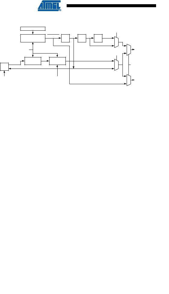
Figure 19-2. Clock Generation Logic, Block Diagram |
|
||||
|
|
UBRRn |
|
|
U2Xn |
|
|
|
foscn |
|
|
|
|
|
|
|
|
|
|
Prescaling |
UBRRn+1 |
/4 |
/2 |
|
|
Down-Counter |
/2 |
||
|
|
|
|
0 |
|
|
|
|
|
|
1 |
|
|
OSC |
|
|
0 |
|
|
|
|
txclk |
|
|
|
|
|
|
1 |
|
|
|
|
|
DDR_XCKn |
|
|
Sync |
Edge |
|
|
|
xcki |
Register |
Detector |
|
0 |
XCKn |
xcko |
|
|
|
UMSELn |
Pin |
|
|
|
1 |
|
|
|
|
|
|
|
DDR_XCKn |
|
|
UCPOLn |
|
1 |
|
|
|
|
|
rxclk |
|
|
|
|
|
0 |
Signal description: |
|
txclk |
Transmitter clock (Internal Signal). |
rxclk |
Receiver base clock (Internal Signal). |
xcki |
Input from XCK pin (internal Signal). Used for synchronous slave |
operation. |
|
xcko |
Clock output to XCK pin (Internal Signal). Used for synchronous master |
|
operation. |
fosc |
XTAL pin frequency (System Clock). |
19.3.1Internal Clock Generation – The Baud Rate Generator
Internal clock generation is used for the asynchronous and the synchronous master modes of operation. The description in this section refers to Figure 19-2.
The USART Baud Rate Register (UBRRn) and the down-counter connected to it function as a programmable prescaler or baud rate generator. The down-counter, running at system clock (fosc), is loaded with the UBRRn value each time the counter has counted down to zero or when the UBRRnL Register is written. A clock is generated each time the counter reaches zero. This clock is the baud rate generator clock output (= fosc/(UBRRn+1)). The Transmitter divides the baud rate generator clock output by 2, 8 or 16 depending on mode. The baud rate generator output is used directly by the Receiver’s clock and data recovery units. However, the recovery units use a state machine that uses 2, 8 or 16 states depending on mode set by the state of the UMSELn, U2Xn and DDR_XCKn bits.
174 ATmega48/88/168 
2545M–AVR–09/07

 ATmega48/88/168
Table 19-1 contains equations for calculating the baud rate (in bits per second) and for calculating the UBRRn value for each mode of operation using an internally generated clock source.
Table 19-1. |
Equations for Calculating Baud Rate Register Setting |
|
|
|||
|
|
Equation for Calculating Baud |
Equation for Calculating |
|||
Operating Mode |
Rate(1) |
UBRRn Value |
||||
|
|
|
|
UBRRn = |
fOSC |
|
|
|
|
|
-----------------------16BAUD – 1 |
||
Asynchronous Normal mode |
BAUD = |
fOSC |
|
|
|
|
(U2Xn = 0) |
|
|
|
|
|
|
|
16(UBRRn + 1) |
|
|
|
||
|
|
|
|
|
|
|
|
|
|
|
UBRRn = |
fOSC |
– 1 |
|
|
|
|
8-------------------BAUD- |
||
Asynchronous Double Speed |
BAUD = |
fOSC |
|
|
|
|
mode (U2Xn = 1) |
(UBRRn + 1) |
|
|
|
||
8 |
|
|
|
|||
|
|
|
|
|
|
|
|
|
|
|
UBRRn = |
fOSC |
– 1 |
|
|
|
|
2-------------------BAUD- |
||
Synchronous Master mode |
BAUD = -------------------------------------- |
fOSC |
|
|
|
|
|
|
2 |
(UBRRn + 1) |
|
|
|
|
|
|
|
|
||
Note: 1. The baud rate is defined to be the transfer rate in bit per second (bps) |
|
|
||||
BAUD |
Baud rate (in bits per second, bps) |
|
|
|
||
fOSC |
System Oscillator clock frequency |
|
|
|
||
UBRRn Contents of the UBRRnH and UBRRnL Registers, (0-4095)
Some examples of UBRRn values for some system clock frequencies are found in Table 19-9 (see page 196).
19.3.2Double Speed Operation (U2Xn)
The transfer rate can be doubled by setting the U2Xn bit in UCSRnA. Setting this bit only has effect for the asynchronous operation. Set this bit to zero when using synchronous operation.
Setting this bit will reduce the divisor of the baud rate divider from 16 to 8, effectively doubling the transfer rate for asynchronous communication. Note however that the Receiver will in this case only use half the number of samples (reduced from 16 to 8) for data sampling and clock recovery, and therefore a more accurate baud rate setting and system clock are required when this mode is used. For the Transmitter, there are no downsides.
175
2545M–AVR–09/07