- •Features
- •1. Pin Configurations
- •1.1 Pin Descriptions
- •1.1.3 Port B (PB7:0) XTAL1/XTAL2/TOSC1/TOSC2
- •1.1.4 Port C (PC5:0)
- •1.1.5 PC6/RESET
- •1.1.6 Port D (PD7:0)
- •1.1.8 AREF
- •1.1.9 ADC7:6 (TQFP and QFN/MLF Package Only)
- •2. Overview
- •2.1 Block Diagram
- •2.2 Comparison Between ATmega48, ATmega88, and ATmega168
- •3. Resources
- •4. Data Retention
- •5. About Code Examples
- •6. AVR CPU Core
- •6.1 Overview
- •6.2 Architectural Overview
- •6.4 Status Register
- •6.5 General Purpose Register File
- •6.6 Stack Pointer
- •6.7 Instruction Execution Timing
- •6.8 Reset and Interrupt Handling
- •6.8.1 Interrupt Response Time
- •7. AVR Memories
- •7.1 Overview
- •7.3 SRAM Data Memory
- •7.3.1 Data Memory Access Times
- •7.4 EEPROM Data Memory
- •7.4.1 EEPROM Read/Write Access
- •7.4.2 Preventing EEPROM Corruption
- •7.5 I/O Memory
- •7.5.1 General Purpose I/O Registers
- •7.6 Register Description
- •8. System Clock and Clock Options
- •8.1 Clock Systems and their Distribution
- •8.2 Clock Sources
- •8.2.1 Default Clock Source
- •8.2.2 Clock Startup Sequence
- •8.3 Low Power Crystal Oscillator
- •8.4 Full Swing Crystal Oscillator
- •8.5 Low Frequency Crystal Oscillator
- •8.6 Calibrated Internal RC Oscillator
- •8.7 128 kHz Internal Oscillator
- •8.8 External Clock
- •8.9 Clock Output Buffer
- •8.10 Timer/Counter Oscillator
- •8.11 System Clock Prescaler
- •8.12 Register Description
- •9. Power Management and Sleep Modes
- •9.1 Sleep Modes
- •9.2 Idle Mode
- •9.3 ADC Noise Reduction Mode
- •9.4 Power-down Mode
- •9.5 Power-save Mode
- •9.6 Standby Mode
- •9.7 Power Reduction Register
- •9.8 Minimizing Power Consumption
- •9.8.1 Analog to Digital Converter
- •9.8.2 Analog Comparator
- •9.8.4 Internal Voltage Reference
- •9.8.5 Watchdog Timer
- •9.8.6 Port Pins
- •9.9 Register Description
- •10. System Control and Reset
- •10.1 Resetting the AVR
- •10.2 Reset Sources
- •10.3 Power-on Reset
- •10.4 External Reset
- •10.6 Watchdog System Reset
- •10.7 Internal Voltage Reference
- •10.8 Watchdog Timer
- •10.8.1 Features
- •10.9 Register Description
- •11. Interrupts
- •11.1 Overview
- •11.2 Interrupt Vectors in ATmega48
- •11.3 Interrupt Vectors in ATmega88
- •11.4 Interrupt Vectors in ATmega168
- •11.4.1 Moving Interrupts Between Application and Boot Space, ATmega88 and ATmega168
- •11.5 Register Description
- •12. External Interrupts
- •12.1 Pin Change Interrupt Timing
- •12.2 Register Description
- •13. I/O-Ports
- •13.1 Overview
- •13.2 Ports as General Digital I/O
- •13.2.1 Configuring the Pin
- •13.2.2 Toggling the Pin
- •13.2.3 Switching Between Input and Output
- •13.2.4 Reading the Pin Value
- •13.2.5 Digital Input Enable and Sleep Modes
- •13.2.6 Unconnected Pins
- •13.3 Alternate Port Functions
- •13.3.1 Alternate Functions of Port B
- •13.3.2 Alternate Functions of Port C
- •13.3.3 Alternate Functions of Port D
- •13.4 Register Description
- •14. 8-bit Timer/Counter0 with PWM
- •14.1 Features
- •14.2 Overview
- •14.2.1 Definitions
- •14.2.2 Registers
- •14.3 Timer/Counter Clock Sources
- •14.4 Counter Unit
- •14.5 Output Compare Unit
- •14.5.1 Force Output Compare
- •14.5.2 Compare Match Blocking by TCNT0 Write
- •14.5.3 Using the Output Compare Unit
- •14.6 Compare Match Output Unit
- •14.6.1 Compare Output Mode and Waveform Generation
- •14.7 Modes of Operation
- •14.7.1 Normal Mode
- •14.7.2 Clear Timer on Compare Match (CTC) Mode
- •14.7.3 Fast PWM Mode
- •14.7.4 Phase Correct PWM Mode
- •14.8 Timer/Counter Timing Diagrams
- •14.9 Register Description
- •15. 16-bit Timer/Counter1 with PWM
- •15.1 Features
- •15.2 Overview
- •15.2.1 Registers
- •15.2.2 Definitions
- •15.3.1 Reusing the Temporary High Byte Register
- •15.4 Timer/Counter Clock Sources
- •15.5 Counter Unit
- •15.6 Input Capture Unit
- •15.6.1 Input Capture Trigger Source
- •15.6.2 Noise Canceler
- •15.6.3 Using the Input Capture Unit
- •15.7 Output Compare Units
- •15.7.1 Force Output Compare
- •15.7.2 Compare Match Blocking by TCNT1 Write
- •15.7.3 Using the Output Compare Unit
- •15.8 Compare Match Output Unit
- •15.8.1 Compare Output Mode and Waveform Generation
- •15.9 Modes of Operation
- •15.9.1 Normal Mode
- •15.9.2 Clear Timer on Compare Match (CTC) Mode
- •15.9.3 Fast PWM Mode
- •15.9.4 Phase Correct PWM Mode
- •15.9.5 Phase and Frequency Correct PWM Mode
- •15.10 Timer/Counter Timing Diagrams
- •15.11 Register Description
- •16. Timer/Counter0 and Timer/Counter1 Prescalers
- •16.0.1 Internal Clock Source
- •16.0.2 Prescaler Reset
- •16.0.3 External Clock Source
- •16.1 Register Description
- •17. 8-bit Timer/Counter2 with PWM and Asynchronous Operation
- •17.1 Features
- •17.2 Overview
- •17.2.1 Registers
- •17.2.2 Definitions
- •17.3 Timer/Counter Clock Sources
- •17.4 Counter Unit
- •17.5 Output Compare Unit
- •17.5.1 Force Output Compare
- •17.5.2 Compare Match Blocking by TCNT2 Write
- •17.5.3 Using the Output Compare Unit
- •17.6 Compare Match Output Unit
- •17.6.1 Compare Output Mode and Waveform Generation
- •17.7 Modes of Operation
- •17.7.1 Normal Mode
- •17.7.2 Clear Timer on Compare Match (CTC) Mode
- •17.7.3 Fast PWM Mode
- •17.7.4 Phase Correct PWM Mode
- •17.8 Timer/Counter Timing Diagrams
- •17.9 Asynchronous Operation of Timer/Counter2
- •17.10 Timer/Counter Prescaler
- •17.11 Register Description
- •18.1 Features
- •18.2 Overview
- •18.3 SS Pin Functionality
- •18.3.1 Slave Mode
- •18.3.2 Master Mode
- •18.4 Data Modes
- •18.5 Register Description
- •19. USART0
- •19.1 Features
- •19.2 Overview
- •19.3 Clock Generation
- •19.3.2 Double Speed Operation (U2Xn)
- •19.3.3 External Clock
- •19.3.4 Synchronous Clock Operation
- •19.4 Frame Formats
- •19.4.1 Parity Bit Calculation
- •19.5 USART Initialization
- •19.6.1 Sending Frames with 5 to 8 Data Bit
- •19.6.2 Sending Frames with 9 Data Bit
- •19.6.3 Transmitter Flags and Interrupts
- •19.6.4 Parity Generator
- •19.6.5 Disabling the Transmitter
- •19.7.1 Receiving Frames with 5 to 8 Data Bits
- •19.7.2 Receiving Frames with 9 Data Bits
- •19.7.3 Receive Compete Flag and Interrupt
- •19.7.4 Receiver Error Flags
- •19.7.5 Parity Checker
- •19.7.6 Disabling the Receiver
- •19.7.7 Flushing the Receive Buffer
- •19.8 Asynchronous Data Reception
- •19.8.1 Asynchronous Clock Recovery
- •19.8.2 Asynchronous Data Recovery
- •19.8.3 Asynchronous Operational Range
- •19.9.1 Using MPCMn
- •19.10 Register Description
- •19.11 Examples of Baud Rate Setting
- •20. USART in SPI Mode
- •20.1 Features
- •20.2 Overview
- •20.3 Clock Generation
- •20.4 SPI Data Modes and Timing
- •20.5 Frame Formats
- •20.5.1 USART MSPIM Initialization
- •20.6 Data Transfer
- •20.6.1 Transmitter and Receiver Flags and Interrupts
- •20.6.2 Disabling the Transmitter or Receiver
- •20.7 AVR USART MSPIM vs. AVR SPI
- •20.8 Register Description
- •20.8.5 USART MSPIM Baud Rate Registers - UBRRnL and UBRRnH
- •21. 2-wire Serial Interface
- •21.1 Features
- •21.2.1 TWI Terminology
- •21.2.2 Electrical Interconnection
- •21.3 Data Transfer and Frame Format
- •21.3.1 Transferring Bits
- •21.3.2 START and STOP Conditions
- •21.3.3 Address Packet Format
- •21.3.4 Data Packet Format
- •21.3.5 Combining Address and Data Packets into a Transmission
- •21.5 Overview of the TWI Module
- •21.5.1 SCL and SDA Pins
- •21.5.2 Bit Rate Generator Unit
- •21.5.3 Bus Interface Unit
- •21.5.4 Address Match Unit
- •21.5.5 Control Unit
- •21.6 Using the TWI
- •21.7 Transmission Modes
- •21.7.1 Master Transmitter Mode
- •21.7.2 Master Receiver Mode
- •21.7.3 Slave Receiver Mode
- •21.7.4 Slave Transmitter Mode
- •21.7.5 Miscellaneous States
- •21.7.6 Combining Several TWI Modes
- •21.9 Register Description
- •22. Analog Comparator
- •22.1 Overview
- •22.2 Analog Comparator Multiplexed Input
- •22.3 Register Description
- •23. Analog-to-Digital Converter
- •23.1 Features
- •23.2 Overview
- •23.3 Starting a Conversion
- •23.4 Prescaling and Conversion Timing
- •23.5 Changing Channel or Reference Selection
- •23.5.1 ADC Input Channels
- •23.5.2 ADC Voltage Reference
- •23.6 ADC Noise Canceler
- •23.6.1 Analog Input Circuitry
- •23.6.2 Analog Noise Canceling Techniques
- •23.6.3 ADC Accuracy Definitions
- •23.7 ADC Conversion Result
- •23.8 Register Description
- •23.8.3.1 ADLAR = 0
- •23.8.3.2 ADLAR = 1
- •24. debugWIRE On-chip Debug System
- •24.1 Features
- •24.2 Overview
- •24.3 Physical Interface
- •24.4 Software Break Points
- •24.5 Limitations of debugWIRE
- •24.6 Register Description
- •25. Self-Programming the Flash, ATmega48
- •25.1 Overview
- •25.1.1 Performing Page Erase by SPM
- •25.1.2 Filling the Temporary Buffer (Page Loading)
- •25.1.3 Performing a Page Write
- •25.2.1 EEPROM Write Prevents Writing to SPMCSR
- •25.2.2 Reading the Fuse and Lock Bits from Software
- •25.2.3 Preventing Flash Corruption
- •25.2.4 Programming Time for Flash when Using SPM
- •25.2.5 Simple Assembly Code Example for a Boot Loader
- •25.3 Register Description
- •26.1 Features
- •26.2 Overview
- •26.3 Application and Boot Loader Flash Sections
- •26.3.1 Application Section
- •26.5 Boot Loader Lock Bits
- •26.6 Entering the Boot Loader Program
- •26.8.1 Performing Page Erase by SPM
- •26.8.2 Filling the Temporary Buffer (Page Loading)
- •26.8.3 Performing a Page Write
- •26.8.4 Using the SPM Interrupt
- •26.8.5 Consideration While Updating BLS
- •26.8.7 Setting the Boot Loader Lock Bits by SPM
- •26.8.8 EEPROM Write Prevents Writing to SPMCSR
- •26.8.9 Reading the Fuse and Lock Bits from Software
- •26.8.10 Preventing Flash Corruption
- •26.8.11 Programming Time for Flash when Using SPM
- •26.8.12 Simple Assembly Code Example for a Boot Loader
- •26.8.13 ATmega88 Boot Loader Parameters
- •26.8.14 ATmega168 Boot Loader Parameters
- •26.9 Register Description
- •27. Memory Programming
- •27.1 Program And Data Memory Lock Bits
- •27.2 Fuse Bits
- •27.2.1 Latching of Fuses
- •27.3 Signature Bytes
- •27.4 Calibration Byte
- •27.5 Page Size
- •27.6 Parallel Programming Parameters, Pin Mapping, and Commands
- •27.6.1 Signal Names
- •27.7 Parallel Programming
- •27.7.1 Enter Programming Mode
- •27.7.2 Considerations for Efficient Programming
- •27.7.3 Chip Erase
- •27.7.4 Programming the Flash
- •27.7.5 Programming the EEPROM
- •27.7.6 Reading the Flash
- •27.7.7 Reading the EEPROM
- •27.7.8 Programming the Fuse Low Bits
- •27.7.9 Programming the Fuse High Bits
- •27.7.10 Programming the Extended Fuse Bits
- •27.7.11 Programming the Lock Bits
- •27.7.12 Reading the Fuse and Lock Bits
- •27.7.13 Reading the Signature Bytes
- •27.7.14 Reading the Calibration Byte
- •27.7.15 Parallel Programming Characteristics
- •27.8 Serial Downloading
- •27.8.1 Serial Programming Pin Mapping
- •27.8.2 Serial Programming Algorithm
- •27.8.3 Serial Programming Instruction set
- •27.8.4 SPI Serial Programming Characteristics
- •28. Electrical Characteristics
- •28.1 Absolute Maximum Ratings*
- •28.2 DC Characteristics
- •28.3 Speed Grades
- •28.4 Clock Characteristics
- •28.4.1 Calibrated Internal RC Oscillator Accuracy
- •28.4.2 External Clock Drive Waveforms
- •28.4.3 External Clock Drive
- •28.5 System and Reset Characteristics
- •28.7 SPI Timing Characteristics
- •28.8 ADC Characteristics
- •28.9 Parallel Programming Characteristics
- •29. Typical Characteristics
- •29.1 Active Supply Current
- •29.2 Idle Supply Current
- •29.3 Supply Current of I/O modules
- •29.3.0.1 Example 1
- •29.3.0.2 Example 2
- •29.3.0.3 Example 3
- •29.6 Standby Supply Current
- •29.8 Pin Driver Strength
- •29.9 Pin Thresholds and Hysteresis
- •29.10 BOD Thresholds and Analog Comparator Offset
- •29.11 Internal Oscillator Speed
- •29.12 Current Consumption of Peripheral Units
- •29.13 Current Consumption in Reset and Reset Pulse width
- •30. Register Summary
- •31. Instruction Set Summary
- •32. Ordering Information
- •32.1 ATmega48
- •32.2 ATmega88
- •32.3 ATmega168
- •33. Packaging Information
- •34. Errata
- •34.1 Errata ATmega48
- •34.2 Errata ATmega88
- •34.3 Errata ATmega168
- •35. Datasheet Revision History
18. SPI – Serial Peripheral Interface
18.1Features
•Full-duplex, Three-wire Synchronous Data Transfer
•Master or Slave Operation
•LSB First or MSB First Data Transfer
•Seven Programmable Bit Rates
•End of Transmission Interrupt Flag
•Write Collision Flag Protection
•Wake-up from Idle Mode
•Double Speed (CK/2) Master SPI Mode
18.2Overview
The Serial Peripheral Interface (SPI) allows high-speed synchronous data transfer between the
ATmega48/88/168 and peripheral devices or between several AVR devices.
The USART can also be used in Master SPI mode, see “USART in SPI Mode” on page 200. The PRSPI bit in “Minimizing Power Consumption” on page 42 must be written to zero to enable SPI module.
162 ATmega48/88/168
2545M–AVR–09/07
ATmega48/88/168 |
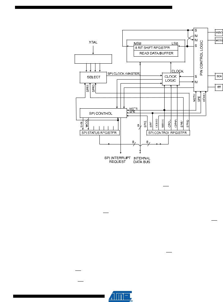
Figure 18-1. SPI Block Diagram(1) |
DIVIDER |
/2/4/8/16/32/64/128 |
SPI2X |
SPI2X |
Note: 1. Refer to Figure 1-1 on page 2, and Table 13-3 on page 79 for SPI pin placement.
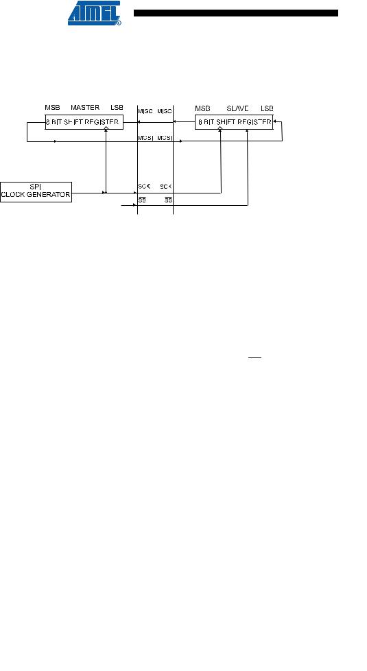
The interconnection between Master and Slave CPUs with SPI is shown in Figure 18-2. The system consists of two shift Registers, and a Master clock generator. The SPI Master initiates the communication cycle when pulling low the Slave Select SS pin of the desired Slave. Master and Slave prepare the data to be sent in their respective shift Registers, and the Master generates the required clock pulses on the SCK line to interchange data. Data is always shifted from Master to Slave on the Master Out – Slave In, MOSI, line, and from Slave to Master on the Master In
– Slave Out, MISO, line. After each data packet, the Master will synchronize the Slave by pulling high the Slave Select, SS, line.
When configured as a Master, the SPI interface has no automatic control of the SS line. This must be handled by user software before communication can start. When this is done, writing a byte to the SPI Data Register starts the SPI clock generator, and the hardware shifts the eight bits into the Slave. After shifting one byte, the SPI clock generator stops, setting the end of Transmission Flag (SPIF). If the SPI Interrupt Enable bit (SPIE) in the SPCR Register is set, an interrupt is requested. The Master may continue to shift the next byte by writing it into SPDR, or signal the end of packet by pulling high the Slave Select, SS line. The last incoming byte will be kept in the Buffer Register for later use.
When configured as a Slave, the SPI interface will remain sleeping with MISO tri-stated as long as the SS pin is driven high. In this state, software may update the contents of the SPI Data Register, SPDR, but the data will not be shifted out by incoming clock pulses on the SCK pin until the SS pin is driven low. As one byte has been completely shifted, the end of Transmission
163
2545M–AVR–09/07
Flag, SPIF is set. If the SPI Interrupt Enable bit, SPIE, in the SPCR Register is set, an interrupt is requested. The Slave may continue to place new data to be sent into SPDR before reading the incoming data. The last incoming byte will be kept in the Buffer Register for later use.
Figure 18-2. SPI Master-slave Interconnection
SHIFT
ENABLE
The system is single buffered in the transmit direction and double buffered in the receive direction. This means that bytes to be transmitted cannot be written to the SPI Data Register before the entire shift cycle is completed. When receiving data, however, a received character must be read from the SPI Data Register before the next character has been completely shifted in. Otherwise, the first byte is lost.
In SPI Slave mode, the control logic will sample the incoming signal of the SCK pin. To ensure correct sampling of the clock signal, the minimum low and high periods should be:
Low periods: Longer than 2 CPU clock cycles.
High periods: Longer than 2 CPU clock cycles.
When the SPI is enabled, the data direction of the MOSI, MISO, SCK, and SS pins is overridden according to Table 18-1 on page 164. For more details on automatic port overrides, refer to “Alternate Port Functions” on page 77.
Table 18-1. |
SPI Pin Overrides(Note:) |
|
||
Pin |
Direction, Master SPI |
Direction, Slave SPI |
||
|
|
|
||
MOSI |
User Defined |
Input |
||
|
|
|
||
MISO |
Input |
User Defined |
||
|
|
|
||
SCK |
User Defined |
Input |
||
|
|
|
|
|
|
|
|
User Defined |
Input |
|
SS |
|||
|
|
|
|
|
Note: See “Alternate Functions of Port B” on page 79 for a detailed description of how to define the direction of the user defined SPI pins.
The following code examples show how to initialize the SPI as a Master and how to perform a simple transmission. DDR_SPI in the examples must be replaced by the actual Data Direction Register controlling the SPI pins. DD_MOSI, DD_MISO and DD_SCK must be replaced by the actual data direction bits for these pins. E.g. if MOSI is placed on pin PB3, replace DD_MOSI with DDB3 and DDR_SPI with DDRB.
164 ATmega48/88/168
2545M–AVR–09/07
ATmega48/88/168
Assembly Code Example(1)
SPI_MasterInit:
; Set MOSI and SCK output, all others input
ldi r17,(1<<DD_MOSI)|(1<<DD_SCK) out DDR_SPI,r17
; Enable SPI, Master, set clock rate fck/16 ldi r17,(1<<SPE)|(1<<MSTR)|(1<<SPR0)
out SPCR,r17 ret
SPI_MasterTransmit:
; Start transmission of data (r16) out SPDR,r16
Wait_Transmit:
; Wait for transmission complete in r16, SPSR
sbrs r16, SPIF rjmp Wait_Transmit
ret
C Code Example(1)
void SPI_MasterInit(void)
{
/* Set MOSI and SCK output, all others input */ DDR_SPI = (1<<DD_MOSI)|(1<<DD_SCK);
/* Enable SPI, Master, set clock rate fck/16 */ SPCR = (1<<SPE)|(1<<MSTR)|(1<<SPR0);
}
void SPI_MasterTransmit(char cData)
{
/* Start transmission */ SPDR = cData;
/* Wait for transmission complete */ while(!(SPSR & (1<<SPIF)))
;
}
Note: 1. See ”About Code Examples” on page 9.
165
2545M–AVR–09/07
The following code examples show how to initialize the SPI as a Slave and how to perform a simple reception.
Assembly Code Example(1)
SPI_SlaveInit:
; Set MISO output, all others input
ldi |
r17,(1<<DD_MISO) |
out |
DDR_SPI,r17 |
; Enable SPI |
|
ldi |
r17,(1<<SPE) |
out |
SPCR,r17 |
ret |
|
SPI_SlaveReceive:
; Wait for reception complete sbis SPSR,SPIF
rjmp SPI_SlaveReceive
; Read received data and return in r16,SPDR
ret
C Code Example(1)
void SPI_SlaveInit(void)
{
/* Set MISO output, all others input */ DDR_SPI = (1<<DD_MISO);
/* Enable SPI */ SPCR = (1<<SPE);
}
char SPI_SlaveReceive(void)
{
/* Wait for reception complete */ while(!(SPSR & (1<<SPIF)))
;
/* Return Data Register */ return SPDR;
}
Note: 1. See ”About Code Examples” on page 9.
166 ATmega48/88/168
2545M–AVR–09/07